

Page 1
Jameco Part number 48531
National
Semiconductor
DM54/74S 188
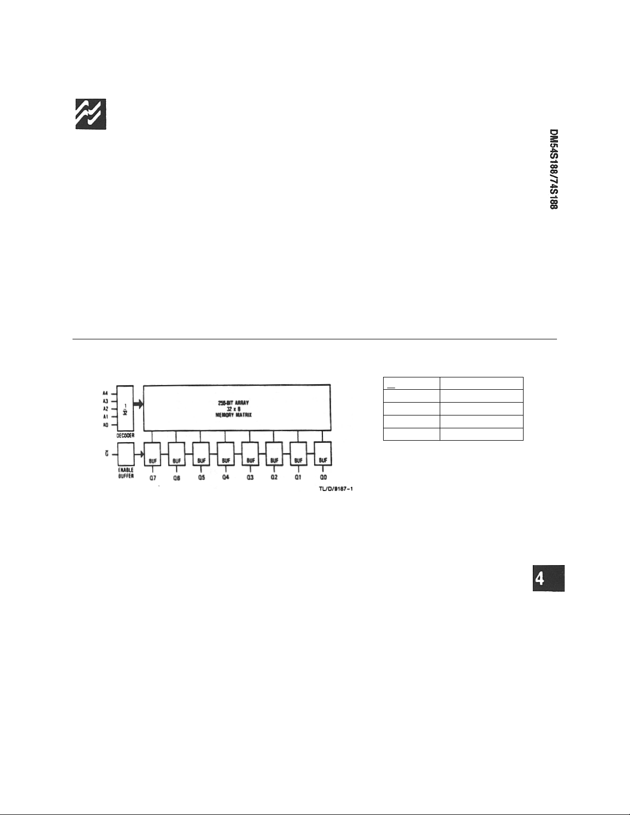
(32 x 8) 256-Bit TTL PROM
General Description
This Schottky memory is org an i zed in t h e popu l ar 32
words by 8 bits configuration. A mem ory en able input
is provided to control the output states. When the
device is enabled, the outputs represen t th e con ten ts of
the selected word. When disabled, the 8 ou tpu ts g o to
the "OFF" or high impedance state.
PROMs are shipped from the factory with low s in all
locations. A high may be programmed into any selected
location by following the programming in structions.
Block Diagram
4-11
Features
!
Advanced titanium-tungsten (Ti-W) fuses
!
Schottky-clamped for high speed
Address access dow n to--25 ns max
Enable access--20 ns max
Enable recovery--20 n s max
!
PNP inputs for reduced input loading
!
All DC and AC param eters g u aran teed ov er
temperature
!
Low voltage TRI-SAFE
!
Open-collector outputs
A0-A4 Addresses
G Output Enable
GND Ground
Q0-Q7 Outputs
Vcc Power Supply
TM
programmin g
Pin Names
Page 2
Jameco Part number 48531
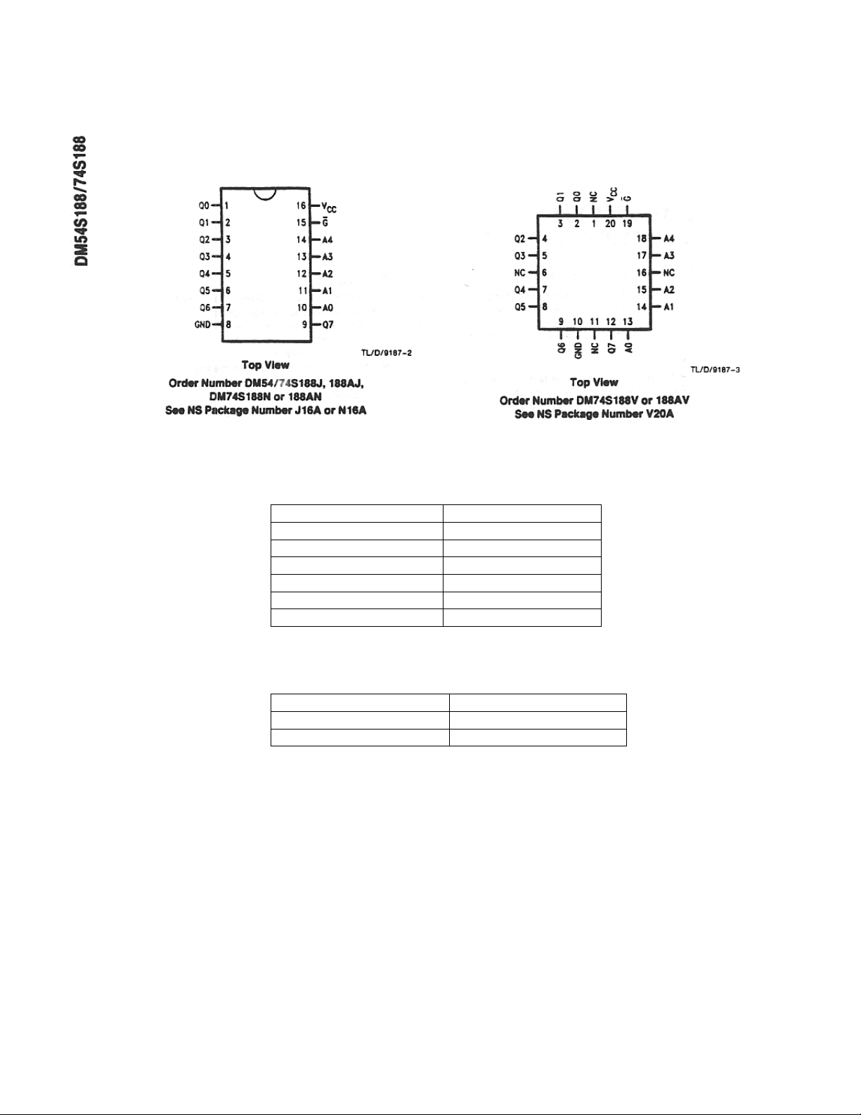
Connection Diagrams
Dual-In-Line Package Plastic Leaded Chip Carrier (PLCC)
Ordering Information
Commercial Temp Range (0
Parameter/Order Number Max Access Time (ns)
DM74S188N 35
DM74S188J 35
DM74S188V 35
DM74S188AN 25
DM74S188AJ 25
DM74S188AV 25
Millitary Temp Range (-55
Parameter/Order Number Max Access Time (ns)
DM54S188J 45
DM54S188AJ 35
4-12
C to + 70
°°°°
C to + 125
°°°°
C)
°°°°
C)
°°°°
Page 3
Jameco Part number 48531
Absolute Maximum Ratings
(Note 1)
If Military/Aerospace specified devices are
required, contact the National Semiconductor Sales
Office/Distributors for availability and
specifications.
Supply Voltag e (N ote 2) -0.5V to + 7.0V
Input Voltage (Note 2) -1.2V to + 5.5V
Output Voltage (Not e 2) -0.5V to + 5.5V
Storage Temperature -65°C to + 150°C
Lead Temp. (Soldering, 10 s econ ds ) 300°C
Operating Conditions
Min Max Units
Supply Voltag e (V
CC
)
Military 4.50 5.50 V
Commercial 4.75 5.25 V
Ambient Temperature (T
)
A
Military -55 +125°C
Commercial 0 + 70°C
Logical "0" Input Voltage 0 0.8 V
Logical "1" Input Voltage 2.0 5.5 V
ESD to be determined
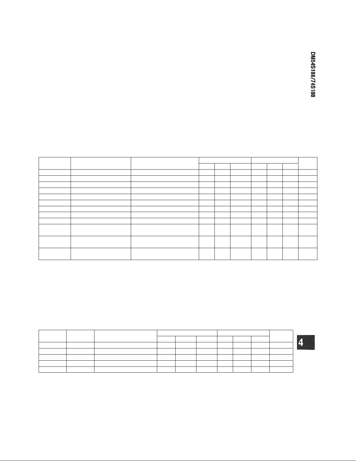
DC Electrical Characteristics
Symbol Parameter Conditions
I
IL
I
IH
V
OL
VIL (Note 4) Low Level Input Voltage 0.80 0.80 V
VIH (Note 4) High Level Input V o ltage 2.0 2.0 V
I
OZ
V
C
C
I
C
O
I
CC
Note 1: Absolute Maximum Ratings ar e tho s e values bey o nd which the device may be permane ntl y damaged. The y do not mean that the device may
be oper ated at these values.
Note 2: These limits do not apply during programming. For the programming r ating s , r e f er to the prog ram m ing ins tr uctio ns.
Note 3: These limits apply over the entire operating range unless stated otherwise. All typical values are for V
Note 4: These are absolute v o l tag e s with respect to pin 8 on the device and include al l overshoots due to system and/or teste r no ise . Do no t attem pt to
test these values without suitabl e equipment.
Input Lo ad Cur r ent Vcc = Max, V
Input Le akage Current VCC = Max, VIN = 2.7V 25 25
Low Level Output Voltage VCC = Min, IOL = 16 mA 0.35 0.50 0.35 0.45 V
Output Leakage Cur r ent VCC = Max, V
(Open-Collector Only) VCC = Max, V
Input Clamp Vo l tag e VCC = Min, IIN = -18 mA -0.8 -1.2 -0.8 -1.2 V
Input Capacitance VCC = 5.0V, VIN = 2.0V
Output Capacitance VCC = 5.0V, VO = 2.0V
Power S upply Current VCC = Max, Input Gr ounded All
(Note 3)
DM54S188 DM74S188
Min Typ Max Min Typ Max
= 0.45v -80 -250 -80 -250
IN
VCC = Max, VIN = 5.5V 1.0 1.0 mA
= 2.4V 50 50
CEX
= 5.5V 100 100
CEX
4.0 4.0 pF
T
= 25°C, 1 MHz
A
T
= 25°C, 1 MHz, Outputs ff
A
Outputs Open
6.0 6.0 pF
70 110 70 110 mA
= 5.0V and TA = 25°C.
CC
Units
µA
µA
µA
µA
AC Electrical Characteristics
COMMERCIAL TEMP RANGE
Symbol
TAA TAVQV Address Acce s s T i me 22 35 17 25 ns
TEA T E V Q V Enable Acces s Time 15 20 15 20 ns
TER TEXQX Enable Recove r y Time 15 25 15 20 ns
TZX T E V Q X Output Enable Time 15 20 15 20 ns
TXZ T E X Q Z Output Disable T im e 15 25 15 20 ns
JEDEC
Symbol
with Standard Load and Operating Conditions
(0°C to + 70°C)
Parameter
DM74S188 DM74S188A
Min Typ Max Min Typ Max
Units
4-13
Page 4
Jameco Part number 48531
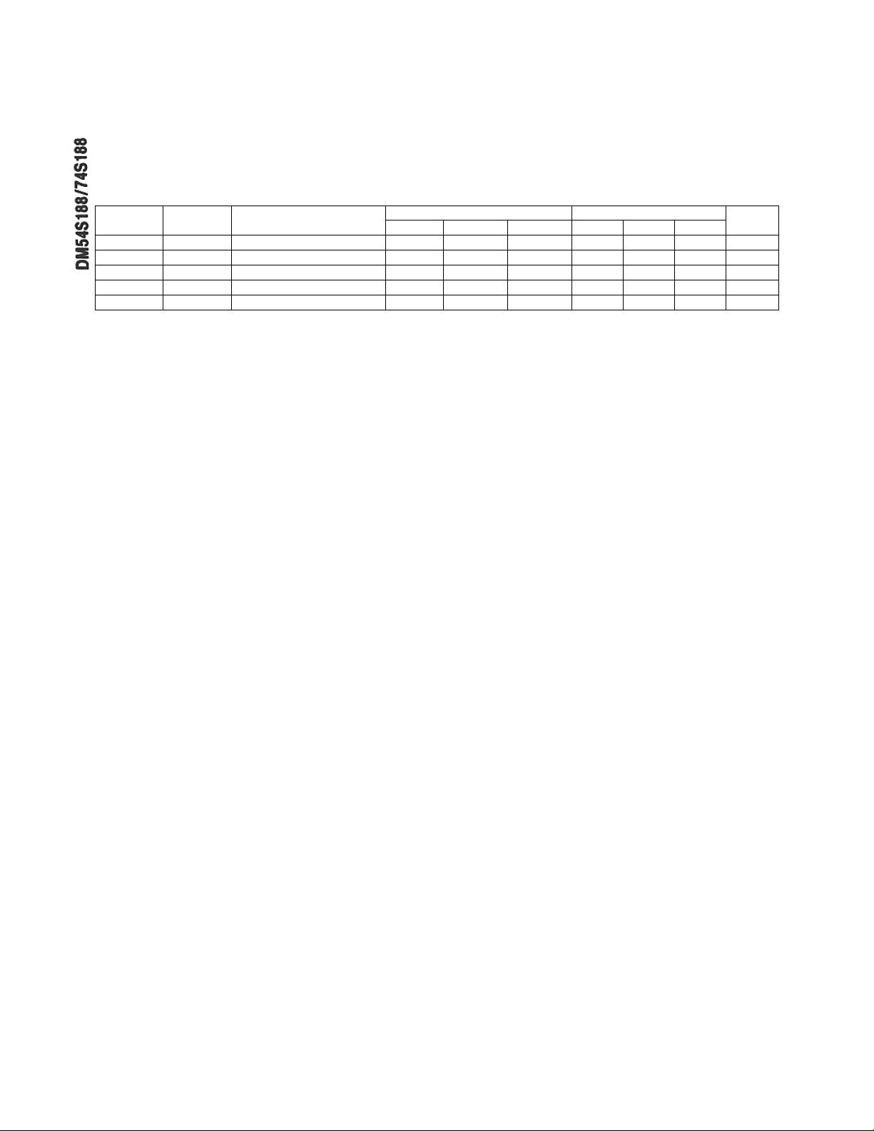
AC Electrical Characteristics
MILITARY TEMP RANGE
Symbol
TAA TAVQV Address Acce s s T i me 22 45 17 35 ns
TEA T E V Q V Enable Acces s Time 15 30 15 30 ns
TER TEXQX Enable Recove r y Time 15 35 15 30 ns
TZX T E V Q X Output Enable Time 15 30 15 30 ns
TXZ T E X Q Z Output Disable T im e 15 35 15 30 ns
JEDEC
Symbol
with Standard Load and Operating Conditions (Continued)
(-55°C to + 125°C)
Parameter
Min Typ Max Min Typ Max
DM54S188 DM54S 188A
Units
Functional Description
TESTABILITY
The Schottky PROM die includes extra row s an d
columns of fusable links for testing the
programmability of each chip. These test fuses are
placed at the worst-case chip location s to prov ide th e
highest possible conf iden ce in th e prog ramming tests in
the final product. A ROM pattern is also permanently
fixed in the additional circuitry and coded to provide a
parity check of input addres s lev els . These an d oth er
TITANIUM-TUNGSTEN FUSES
National's Programm able Read-Only Memories
(PROMs) feature titanium-tungsten (Ti-W) fuse links
designed to program ef ficiently with only 10.5V
applied. The high performance and reliability of these
PROMs are the result of fabrication by a Schottky
bipolar process, of which the titaniumtungsten
metallization is an integral part, and the use of an
on-chip program ming circuit .
test circuits are used to test for correct operation of the
row and column-select circuits and fu n ctionality of
input and enable gates. All test circuits are available at
both water and as s embled device levels t o all ow 100%
functional and parametric testing at every stage of th e
test flow.
A major advantage of the titanium-tungsten fuse
technology is the low programm in g v oltage of th e f use
links. At 10.5V, this virtually elimin ates th e n eed for
guard-ring devices and wide spacings required for
other fuse technologies. Care is taken, however, to
minimize v oltag e drops across th e die an d to redu ce
RELIABILITY
parasitics. The device is designed to ensure that
worst-case fuse operating current is low enough for
As with all National products, the Ti-W PROMs are
subjected to an on-going reliability evaluation by the
Reliability Assurance Department. These evaluations
employ accelerated life tests, in clu ding dynamic
high-temperature operating life, temperature-humidity
life, temperature cycling, an d th ermal shock. To date,
reliable long-term operation. The Darlington
programming circuit is liberally designed to insure
adequate power density for blowing th e f use lin k s. The
complete circuit design is optimized to provide high
performance over the en tire operatin g ran g es of V
CC
and temperature.
nearly 7.4 million Schottky Ti-W PROM device hours
have been logged, with samples in Epoxy B molded
DIP (N-package), PLCC (V-package) an d CER DIP
(J-package). Device performan ce in all packag e
configurations is excellent.
4-14
 Loading...