

Page 1
LOW VOLTAGE CMOS SINGLE 2-INPUT AND GATE
■ 5V TOLERANT INPUTS
■ HIGH SPEED: t
■ LOW POWER DISSIPATION:
I
=1µA(MAX.)atTA=25°C
CC
■ POWER DOWN PROTECTION ON INPUTS
AND OUTPUTS
■ SYMMETRICAL OUTPUTIMPEDANCE:
|I
|=IOL= 24mA (MIN) at VCC=3V
OH
■ BALANCED PROPAGATION DELAYS:
t
≅ t
PLH
PHL
■ OPERATING VOLTAGE RANGE:
V
(OPR) = 1.65V to 5.5V
CC
(1.2V Data Reten tion)
■ IMPROVED LATCH-UP IMMUNITY
= 4.5ns (MAX.) at VCC=3V
PD
74LX1G08
WITH 5V TOLERANT INPUT
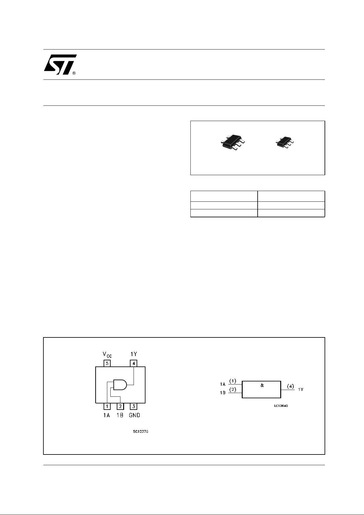
SOT323-5LSOT23-5L
ORDER CODES
PACKAGE T & R
SOT23-5L 74LX1G08STR
SOT323-5L 74LX1G08CTR
DESCRIPTION
The 74LX1G08 is a low voltage CMOS SINGLE
2-INPUT AND GAT E fabricat ed with sub-micron
silicon gate and double-layer me tal wiring C
2
MOS
technology.
It is ideal f or 1.65 to 5.5 V
operations and low
CC
power and low noise applications. The internal
circuit is composed of 3 stages including buffer
PIN CONNECTION AND IEC LOGIC SYMBOLS
output, which provide high noise immunity and
stable output.
Powerdownprotectionisprovidedoninputand
output and 0 to 7V can be accepted on inputs with
no regard to the supply voltage. It can be
interfaced to 5V signal e nvironment for inputs in
mixed 3.3/5V system.
All inputs and outputs are equipped with
protection circuits against static discharge.
1/10April 2004
Page 2
74LX1G08
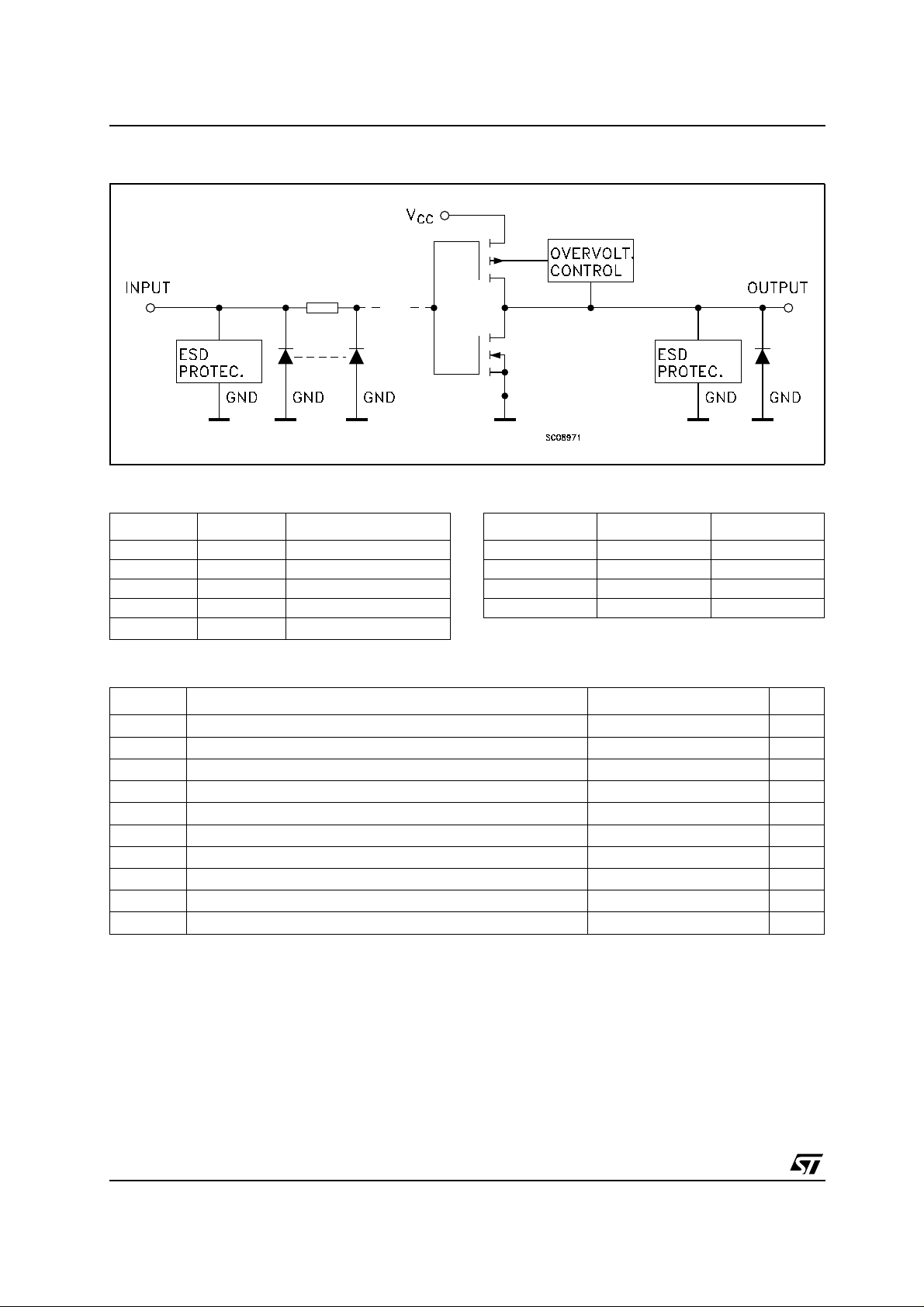
INPUT AND OUTPUT EQUIVALENT CIRCUIT
PIN DESCRIPTION TRUTH TABLE
PIN N° SYMBOL NAME AND FUNCTION
1 1A Data Input
2 1B Data Input
3 GND Ground (0V)
4 1Y Data Output
5
V
CC
Positive Supply Voltage
ABY
LLL
LHL
HLL
HHH
ABSOLUTE MAXIMUM RATINGS
Symbol Parameter Value Unit
V
V
V
V
I
I
OK
I
or I
I
CC
T
T
Absolute Maximum Ratings are those values beyond which damage to the device may occur. Functional operation under these conditions is
not implied
absolute maximum rating must be observed
1) I
O
2) V
<GND,VO>V
O
Supply Voltage
CC
DC Input Voltage
I
DC Output Voltage (VCC=0V)
O
DC Output Voltage (High or Low State) (note 1) -0.5 to VCC+0.5
O
DC Input Diode Current
IK
DC Output Diode Current (note 2)
DC Output Current
O
DC VCCor Ground Current per Supply Pin
GND
Storage Temperature
stg
Lead Temperature (10 sec)
L
CC
-0.5 to +7.0 V
-0.5 to +7.0 V
-0.5 to +7.0 V
V
-50 mA
-50 mA
± 50 mA
± 50 mA
-65 to +150 °C
300 °C
2/10
Page 3
74LX1G08
RECOMMENDED OPERATING CONDITIONS
Symbol Parameter Value Unit
V
V
V
V
I
OH,IOL
I
OH,IOL
I
OH,IOL
I
OH,IOL
I
OH,IOL
T
dt/dv Input Rise and Fall Time (note 2) 0 to 10 ns/V
1) Truth Table guaranteed: 1.2V to 3.6V
2) V
from0.8V to 2V at VCC=3.0V
IN
DC SPECIFICATIONS
Supply Voltage (note 1)
CC
Input Voltage
I
Output Voltage (VCC=0V)
O
Output Voltage (High or Low State) 0 to V
O
High or Low Level Output Current (VCC=4.5to5.5V)
High or Low Level Output Current (VCC=3.0to3.6V)
High or Low Level Output Current (VCC=2.7to3.0V)
High or Low Level Output Current (VCC=2.3to2.7V)
High or Low Level Output Current (VCC=1.65to2.3V)
Operating Temperature
op
Test Condition Value
1.65 to 5.5 V
0to5.5 V
0to5.5 V
CC
± 32 mA
± 24 mA
± 12 mA
± 8mA
± 4mA
-55 to 125 °C
V
Symbol Parameter
V
V
V
High Level Input
IH
Voltage
V
Low Level Input
IL
Voltage
High Level Output
OH
Voltage
Low Level Output
OL
Voltage
Input Leakage
I
I
Current
I
Power Off Leakage
off
Current
I
Quiescent Supply
CC
Current
V
CC
(V)
1.65 to 1.95
3.0 to 5.5
1.65 to 1.95
3.0 to 5.5
1.65to4.5
1.65
2.3
3.0
4.5
1.65to4.5
1.65
2.3
3.0
4.5
1.65to5.5
0
1.65to5.5
-40 to 85 °C -55 to 125 °C
Min. Max. Min. Max.
0.75V
CC
0.7V
CC
0.7V
CC
0.25V
CC
0.3V
CC
0.3V
CC
=-100 µAVCC-0.1 VCC-0.1
I
O
=-4 mA
I
O
=-8 mA
I
O
I
=-16 mA
O
=-24 mA
I
O
=-32 mA
I
O
IO=100 µA
I
=4 mA
O
=8 mA
I
O
I
=16 mA
O
=24 mA
I
O
I
=32 mA
O
= 0 to 5.5V
V
I
or VO=5.5V
V
I
V
I=VCC
or GND
1.2 1.2
1.9 1.9
2.4 2.4
2.2 2.2
3.8 3.8
0.1 0.1
0.45 0.45
0.3 0.3
0.4 0.4
0.55 0.55
0.55 0.55
± 10 ± 10 µA
10 10 µA
10 10 µA
0.75V
0.7V
0.7V
CC
CC
CC
0.25V
0.3V
0.3V
CC
CC
Unit
V2.3 to 2.7
CC
V2.3 to 2.7
V
V
3/10
Page 4

74LX1G08
AC ELECTRICAL CHARACTERISTICS
Test Condition Value
Symbol Parameter
t
PLHtPHL
Propagation Delay
Time
V
(V)
CC
C
(pF)
R
L
(Ω)
= t
t
L
s
(ns)
1.65 to 1.95
2.3to2.7 27.027.0
3.0to3.6 14.714.7
15 1MΩ 3.0
-40to85°C -55to125°C
r
Min. Max. Min. Max.
212.0212.0
Unit
4.5to5.5 14.114.1
1.65 to 1.95 30 1000 2.0 2 7.5 2 7.5
ns
2.3 to 2.7 30 500 2.0 2 5.5 2 5.5
2.7 50 500 2.5 1 5.2 1 5.2
3.0 to 3.6 50 500 2.5 1 4.2 1 4.2
4.5 to 5.5 50 500 2.5 1 3.7 1 3.7
CAPACITANCE CHARACTERISTICS
Test Condition Value
=25°C
Symbol Parameter
V
CC
(V)
C
C
Input Capacitance
IN
Power Dissipation Capacitance
PD
(note 1)
1.8 fIN=10MHz 21
3.3 26
1) CPDis defined as the value of the IC’s internal equivalent capacitance which is calculated from the operating current consumption without
load. (Refer to Test Circuit). Average current can be obtained by the following equation. I
CC(opr)=CPDxVCCxfIN+ICC
T
A
Min. Typ. Max.
4pF
Unit
pF2.5 24
4/10
Page 5

TEST CIRCUIT
74LX1G08
RT=Z
of pulse generator (typically 50Ω)
OUT
TEST CIRCUIT AND WAVEFORM SYMBOL VALUE
Symbol
C
L
R
L
V
IH
V
M
t
r=tr
1.65 to 1.95V 2.3 to 2.7V 2.7 to 5.5V
15pF/30pF 15pF/30pF 15pF/50pF
1MΩ/1000Ω 1MΩ/500Ω 1MΩ/500Ω
V
CC
VCC/2 VCC/2 VCC/2
<2.0ns <2.0ns <2.5ns
V
V
WAVEFORM: PROPAGATION DELAY (f=1MHz; 50% duty cycle)
CC
CC
V
CC
5/10
Page 6

74LX1G08
SOT23-5L MECHANICAL DATA
mm. mils
DIM.
MIN. TYP MAX. MIN. TYP. MAX.
A 0.90 1.45 35.4 57.1
A1 0.00 0.10 0.0 3.9
A2 0.90 1.30 35.4 51.2
b 0.35 0.50 13.7 19.7
C 0.09 0.20 3.5 7.8
D 2.80 3.00 110.2 118.1
E 1.50 1.75 59.0 68.8
e0.95 37.4
H 2.60 3.00 102.3 118.1
L 0.10 0.60 3.9 23.6
.
6/10
7049676C
Page 7

74LX1G08
SOT323-5L MECHANICAL DATA
mm. mils
DIM.
MIN. TYP MAX. MIN. TYP. MAX.
A 0.80 1.10 31.5 43.3
A1 0.00 0.10 0.0 3.9
A2 0.80 1.00 31.5 39.4
b 0.15 0.30 5.9 11.8
C 0.10 0.18 3.9 7.1
D 1.80 2.20 70.9 86.6
E 1.80 2.40 70.9 94.5
E1 1.15 1.35 45.3 53.1
e
e1 1.3 51.2
L 0.10 0.30 3.9 11.8
.65
0
25.6
7/10
Page 8

74LX1G08
Tape & Reel SOT23-xL MECHANICAL DATA
DIM.
MIN. TYP MAX. MIN. TYP. MAX.
A 180 7.086
C 12.8 13.0 13.2 0.504 0.512 0.519
D 20.2 0.795
N 60 2.362
T 14.4 0.567
Ao 3.13 3.23 3.33 0.123 0.127 0.131
Bo 3.07 3.17 3.27 0.120 0.124 0.128
Ko 1.27 1.37 1.47 0.050 0.054 0.0.58
Po 3.9 4.0 4.1 0.153 0.157 0.161
P 3.9 4.0 4.1 0.153 0.157 0.161
mm. inch
8/10
Page 9

Tape & Reel SOT323-xL MECHANICAL DATA
74LX1G08
DIM.
MIN. TYP MAX. MIN. TYP. MAX.
A 175 180 185 6.889 7.086 7.283
C 12.8 13 13.2 0.504 0.512 0.519
D 20.2 0.795
N 59.5 60 60.5 2.362
T 14.4 0.567
Ao 2.25 0.088
Bo 2.7 0.106
Ko 1.2 0.047
Po 3.9 4 4.1 0.153 0.157 0.161
P 3.8 4 4.2 0.149 0.157 0.165
mm. inch
9/10
Page 10

74LX1G08
Information furnished is believed to be accurate and reliable. However, STMicroelectronics assumes no responsibility for the
consequences of use of such inform ation nor fo r an y infring ement of p atents or o ther rights of third p arties which may r esult f rom
its use. No license is granted by implication or otherwise under any patent or patent rights of STMicroelectronics. Specifications
mentioned in this publication are subject to change without notice. This publication supersedes and replaces all information
previously supplied. STMicroelectronics products are not authorized for use as critical components in life support devices or
systems without express written approval of STMicroelectronics.
Australia - Belgium - Brazil - Canada - China - Czech Republic - Finland - France - Germany - Hong Kong - India - Israel - Italy - Japan -
Malaysia - Malta - Morocco - Singapore - Spain - Sweden - Switzerland - United Kingdom - United States.
The ST logo is a registered trademark of STMicroelectronics
All other names are the property of their respective owners
© 2004 STMicroelectronics - All Rights Reserved
STMicroelectronics GROUP OF COMPANIES
http://www.st.com
10/10
 Loading...