

Page 1
1/10September 2003
■ 5V TOLERANT INPUTS
■ HIGH SPEED: t
PD
= 4.7ns (MAX.) at VCC=3V
■ LOW POWER DISSIPATION:
I
CC
=1µA(MAX.)atTA=25°C
■ POWER DOWN P ROT ECTION ON I NP UTS
AND OUTPUTS
■ SYMMETRICAL OUTPUT IMPEDANCE:
|I
OH
|=IOL= 24m A (MIN) at VCC=3V
■ BALANCED PROPAGATION DELAYS:
t
PLH
≅ t
PHL
■ OPERATING V OLTAGE RANGE:
V
CC
(OPR) = 1.65V to 5.5V
(1.2V Data Retention)
■ LATCH-UP PE RFORMANCE EXCEED
300mA
DESCRIPTION
The 74LX1G04 is a low voltage CMOS SINGLE
INVERTER fabricated with sub-mi cron silic on
gate and double-layer metal wiring C
2
MOS
tecnology.
It is ideal for 1.65 to 5.5 V
CC
operations and low
power and low noise a pplications. The i nterna l
circuit is composed of 3 stages including buffer
output, which provide high noise immunity and
stable output. Power down protection is provided
on input and output and 0 to 7V c an be accepted
on input with no regard to the supply voltage. T his
device can be used to interface 5V to 3V or lower
power supply system. The sub-m icron CMOS
technology used allow low power consumption
and guarantee optimized operation bet ween 2.8V
and 1.8V system, as Smart P hone, Digital Still
Camera, PDA, Notebook, or each battery
powered equipment.
All input and outputs are equipped with protection
circuits against ESD discharge.
74LX1G04
LOW VOLTAGE CMOS SINGLE INVERTER
WITH 5V TOLERANT INPUT
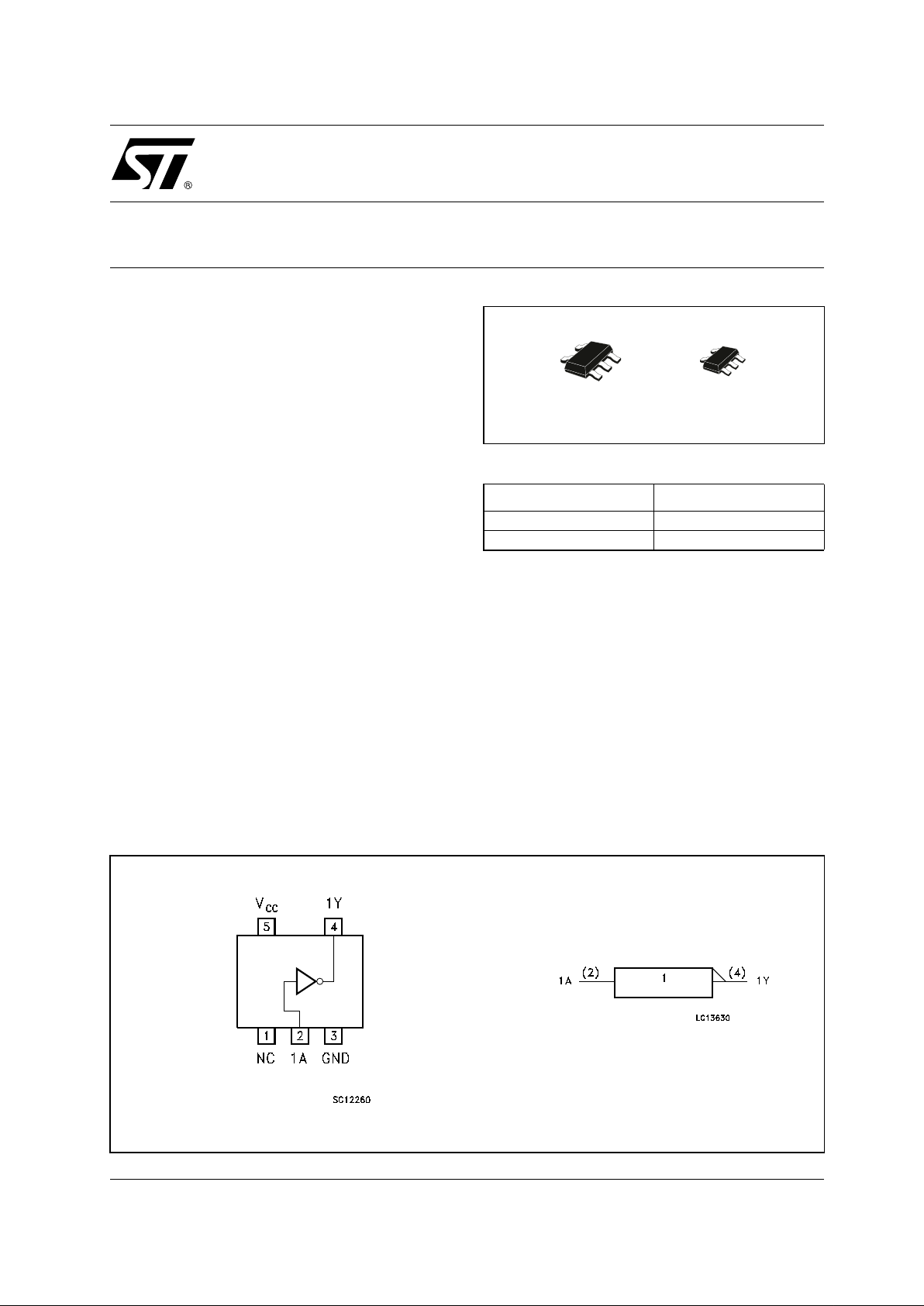
PIN CONNECTION AND IEC LOGIC SYMBOLS (top view)
ORDER CODES
PACKAGE T & R
SOT23-5L 74LX1G04STR
SOT323-5L 74LX1G04CTR
SOT323-5LSOT23-5L
Page 2
74LX1G04
2/10
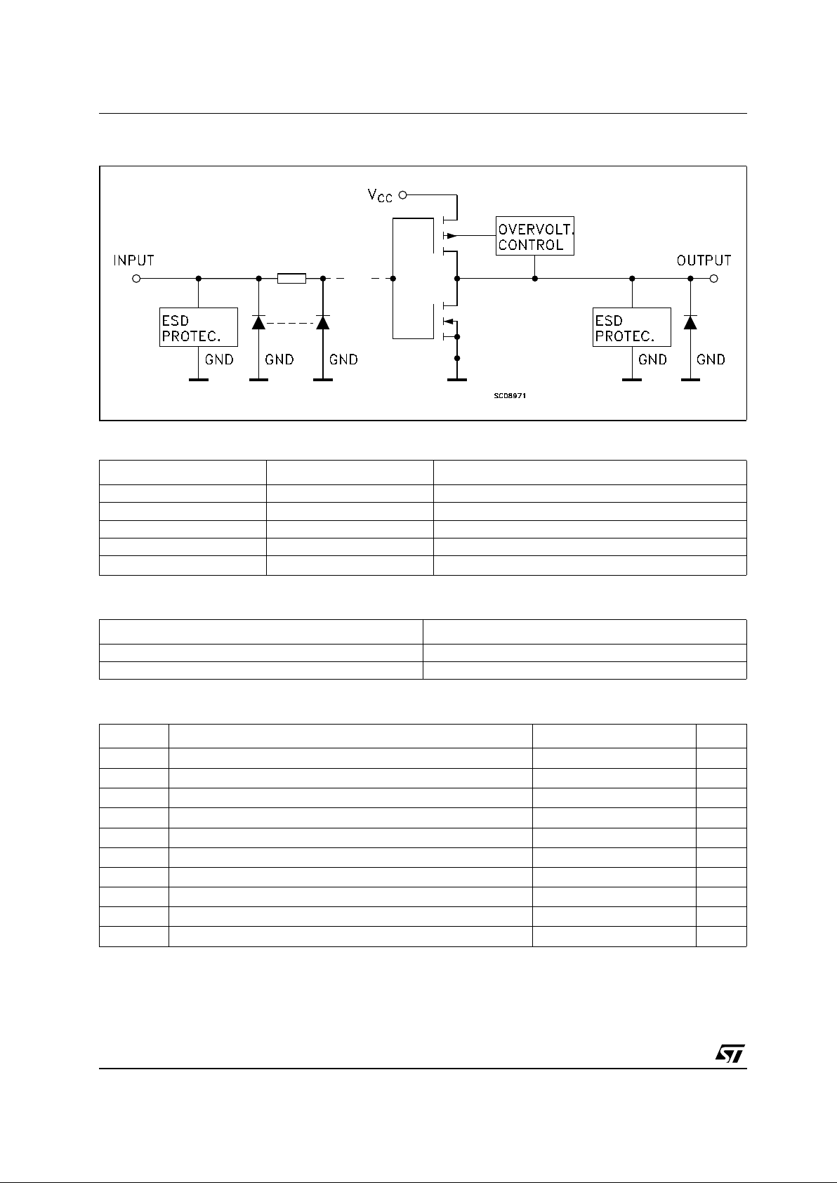
INPUT AND OUTPUT E QUIVALENT CIRCUIT
PIN DESCRIPTION
TRUTH T ABLE
ABSOLUTE MAXIMUM RATINGS
Absolute Maximum Rating are those value beyond which damage to the device may occur. Functional operation under these condition isnot
implied
1) I
O
absolute maximum rating must be observed
2) V
O
<GND
PIN N° SYMBOL NAME AND FUNCTION
1 N.C. Not connected
2 1A Data Inputs
4 1Y Data Outputs
3 GND Ground (0V)
5
V
CC
Positive Supply Voltage
AY
LH
HL
Symbol Parameter² Value Unit
V
CC
Supply Voltage
-0.5 to +7.0 V
V
I
DC Input Voltage
-0.5 to +7.0 V
V
O
DC Output Voltage (VCC= 0V)
-0.5 to +7.0 V
V
O
DC Output Voltage (High or Low State) (note 1) -0.5 to VCC+ 0.5
V
I
IK
DC Input Diode Current
-50 mA
I
OK
DC Output Diode Current (note 2)
-50 mA
I
O
DC Output Current
± 50 mA
I
CC
or I
GND
DC VCCor Ground Current per Supply Pin
± 50 mA
T
stg
Storage Temperature
-65 to +150 °C
T
L
Lead Temperature (10 sec)
260 °C
Page 3
74LX1G04
3/10
RECOMMENDED OPERATING CONDITIONS
1) Truth Table guaranteed: 1.2V to 5.5V
2) V
IN
from0.8V to 2Vat VCC=3.0V
DC S PEC IFICATION
Symbol Parameter Value Unit
V
CC
Supply Voltage (note 1)
1.65 to 5.5 V
V
I
Input Voltage
0 to 5.5 V
V
O
Output Voltage (VCC= 0V)
0 to 5.5 V
V
O
Output Voltage (High or Low State) 0 to V
CC
V
I
OH,IOL
High or Low Level Output Current (VCC= 4.5 to 5.5V)
± 32 mA
I
OH,IOL
High or Low Level Output Current (VCC= 3.0 to 3.6V)
± 24 mA
I
OH,IOL
High or Low Level Output Current (VCC= 2.7 to 3.0V)
± 16 mA
I
OH,IOL
High or Low Level Output Current (VCC= 2.3 to 2.7V)
± 8mA
I
OH,IOL
High or Low Level Output Current (VCC= 1.65 to 2.3V)
± 4mA
T
op
Operating Temperature
-55 to 125 °C
dt/dv
Input Rise and Fall Time
(note 2)
(V
CC
= 3.0 to 5.5V)
0to10
ns/V
(V
CC
= 1.65 to 2.7V)
0to20
Symbol Parameter
Test Condition Value
Unit
V
CC
(V)
-40 to 85 °C -55 to 125 °C
Min. Max. Min. Max.
V
IH
High Level Input
Voltage
1.65 to 1.95
0.75V
CC
0.75V
CC
V2.3 to 2.7
0.7V
CC
0.7V
CC
3.0 to 5.5
0.7V
CC
0.7V
CC
V
IL
Low Level Input
Voltage
1.65 to 1.95
0.25V
CC
0.25V
CC
V2.3 to 2.7
0.3V
CC
0.3V
CC
3.0 to 5.5
0.3V
CC
0.3V
CC
V
OH
High Level Output
Voltage
1.65 to 4.5
IO=-100 µAVCC-0.1 VCC-0.1
V
1.65
I
O
=-4 mA
1.2 1.2
2.3
I
O
=-8 mA
1.9 1.9
3.0
I
O
=-16 mA
2.4 2.4
I
O
=-24 mA
2.2 2.2
4.5
I
O
=-32 mA
3.8 3.8
V
OL
Low Level Output
Voltage
1.65 to 4.5
IO=100 µA
0.1 0.1
V
1.65
I
O
=4 mA
0.45 0.45
2.3
I
O
=8 mA
0.3 0.3
3.0
I
O
=16 mA
0.4 0.4
I
O
=24 mA
0.55 0.55
4.5
I
O
=32 mA
0.55 0.55
I
I
Input Leakage
Current
1.65 to 5.5
V
I
= 0 to 5.5V
± 5 ± 10 µA
I
off
Power Off Leakage
Current
0
V
I
or VO= 5.5V
10 10 µA
I
CC
Quiescent Supply
Current
1.65 to 5.5
V
I=VCC
or GND
10 10 µA
Page 4

74LX1G04
4/10
AC ELECT RICAL CHARACTERISTICS
CAPACITANCE CHARACT E RISTICS
1) CPDis defined as the value of the IC’s internal equivalent capacitance which is calculated from the operating current consumption without
load. (Refer to Test Circuit). Average current can be obtained by the following equation. I
CC(opr)=CPDxVCCxfIN+ICC
Symbol Parameter
Test Condition Value
Unit
V
CC
(V)
C
L
(pF)
R
L
(Ω)
t
s
= t
r
(ns)
-40 to 85 °C -55 to 125 °C
Min. Max. Min. Max.
t
PLHtPHL
Propagation Delay
Time
1.65 to 1.95
15 1MΩ 3.0
210211
ns
2.3 to 2.7 2 7.0 2 8.0
3.0 to 3.6 1 4.7 1 5.7
4.5 to 5.5 1 4.1 1 5.1
1.65 to 1.95 30 1000 2.0 2 11 2 12
2.3 to 2.7 30 500 2.0 2 7.5 2 8.5
2.7 50 500 2.5 1 5.5 1 6.5
3.0 to 3.6 50 500 2.5 1 5.2 1 6.2
4.5 to 5.5 50 500 2.5 1 4.2 1 5.2
Symbol Parameter
Test Condition Value
Unit
V
CC
(V)
T
A
=25°C
Min. Typ. Max.
C
IN
Input Capacitance
04pF
C
PD
Power Dissipation Capacitance
(note 1)
1.8 fIN= 10MHz 16
pF2.5 18
3.3 20
Page 5

74LX1G04
5/10
TEST CIRCUIT
RT=Z
OUT
of pulse generator (typically 50Ω)
TEST CIRCUIT AND WAVEFORM SYMBO L VALUE
WAVEFORM: P RO PAGATION DELAY (f=1MHz; 50% duty cycle)
Symbol
V
CC
1.65 to 1.95V 2.3 to 2.7V 2.7 to 5.5V
C
L
15pF/30pF 15pF/30pF 15pF/50pF
R
L
1MΩ/1000Ω 500Ω 500Ω
V
IH
V
CC
V
CC
V
CC
V
M
VCC/2 VCC/2 VCC/2
t
r=tr
<2.0ns <2.0ns <2.5ns
Page 6

74LX1G04
6/10
DIM.
mm. mils
MIN. TYP MAX. MIN. TYP. MAX.
A 0.90 1.45 35.4 57.1
A1 0.00 0.10 0.0 3.9
A2 0.90 1.30 35.4 51.2
b 0.35 0.50 13.7 19.7
C 0.09 0.20 3.5 7.8
D 2.80 3.00 110.2 118.1
E 1.50 1.75 59.0 68.8
e0.95 37.4
H 2.60 3.00 102.3 118.1
L 0.10 0.60 3.9 23.6
SOT23-5L MECHANICAL DATA
7049676C
.
Page 7

74LX1G04
7/10
DIM.
mm. mils
MIN. TYP MAX. MIN. TYP. MAX.
A 0.80 1.10 31.5 43.3
A1 0.00 0.10 0.0 3.9
A2 0.80 1.00 31.5 39.4
b 0.15 0.30 5.9 11.8
C 0.10 0.18 3.9 7.1
D 1.80 2.20 70.9 86.6
E 1.80 2.40 70.9 94.5
E1 1.15 1.35 45.3 53.1
e
.65
25.6
e1 1.3 51.2
L 0.10 0.30 3.9 11.8
SOT323-5L MECHANICAL DATA
0
Page 8

74LX1G04
8/10
DIM.
mm. inch
MIN. TYP MAX. MIN. TYP. MAX.
A 180 7.086
C 12.8 13.0 13.2 0.504 0.512 0.519
D 20.2 0.795
N 60 2.362
T 14.4 0.567
Ao 3.13 3.23 3.33 0.123 0.127 0.131
Bo 3.07 3.17 3.27 0.120 0.124 0.128
Ko 1.27 1.37 1.47 0.050 0.054 0.0.58
Po 3.9 4.0 4.1 0.153 0.157 0.161
P 3.9 4.0 4.1 0.153 0.157 0.161
Tape & Reel SOT23-xL MECHANICAL D ATA
Page 9

74LX1G04
9/10
DIM.
mm. inch
MIN. TYP MAX. MIN. TYP. MAX.
A 175 180 185 6.889 7.086 7.283
C 12.8 13 13.2 0.504 0.512 0.519
D 20.2 0.795
N 59.5 60 60.5 2.362
T 14.4 0.567
Ao 2.25 0.088
Bo 2.7 0.106
Ko 1.2 0.047
Po 3.98 4 4.2 0.156 0.157 0.165
P 3.98 4 4.2 0.156 0.157 0.165
Tape & Reel SOT323-xL MECHANICAL DATA
Page 10

74LX1G04
10/10
Information furnished is believed to be accurate and reliable. However, STMicroelectronics assumes no responsibility for the
consequences of use o f suc h info rmat ion n or for any in fring ement of paten ts or oth er ri ghts of th ird p arties which may resul t f rom
its use. No license is granted by implication or otherwise under any patent or patent rights of STMicroelectronics. Specifications
mentioned in this publication are subject to change without notice. This publication supersedes and replaces all information
previously supplied. STMicroelectronics products are not authorized for use as critical components in life support devices or
systems without express written approval of STMicroelectronics.
The ST logo is a registered trademark of STMicroelectronics
All other names are the property of their respective owners
© 2003 STMicroelectronics - All Rights Reserved
STMicroelectronics GROUP OF COMPANIES
Australia - Belgium - Brazil - Canada - China - Czech Republic - Finland - France - Germany - Hong Kong - India - Israel - Italy - Japan -
Malaysia - Malta - Morocco - Singapore - Spain - Sweden - Switzerland - United Kingdom - United States.
http://www.st.com
 Loading...