

Page 1
1/10July 2001
■ HIGH SPEED:
f
MAX
= 150 MHz (TYP.) at VCC = 3.3V
■ 5V TOLERANT INPUTS
■ POWER-DOWN PROTECTION ON INPUTS
■ INPUT VOLTAGE LEVEL:
V
IL
= 0.8V, VIH = 2V at VCC =3V
■ LOW POWER DISSIPATION:
I
CC
= 4 µA (MAX.) at TA=25°C
■ LOW NOISE:
V
OLP
= 0.3V (TYP.) at VCC =3.3V
■ SYMMETRICAL OUTPUT IMPEDANCE:
|I
OH
| = IOL = 4 mA (MIN) at VCC =3V
■ BALANCED PROPAGATION DELAYS:
t
PLH
≅ t
PHL
■ OPERATING VOLT AG E R ANGE:
V
CC
(OPR) = 2V to 3.6V (1.2V Data Retention)
■ PIN AND FUNCTION COMPATIBLE WITH
74 SERIES 273
■ IMPROVED LATCH-UP IMMUNITY
DESCRIPTION
The 74LVX273 is a low voltage CMOS OCTAL
D-TYPE FLIP-FLOP WITH CLEAR fabricated with
sub-micron silicon gate and double-layer metal
wiring C
2
MOS technology. It is ideal for low
power, battery operated and low noise 3.3V
applications.
Information signals applied to D inputs are
transferred to the Q o utputs on the positive going
edge of the clock pulse.
When the CLE AR
input is held low, the Q outputs
are held low independently of the other inputs.
Power down protection is provided on all inputs
and 0 to 7V can be accepted on inputs with no
regard to the supply voltage.
This device can be used to interface 5V to 3V. It
combines high speed performance with the true
CMOS low power consumption.
All inputs and outputs are equipped with
protection circuits against stat ic discharge, giving
them 2KV ESD immunity and transient excess
voltage.
74LVX273
LOW VOLTAGE CMOS OCTAL D-TYPE FLIP-FLOP
WITH CLEAR (5V TOLERANT INPUTS)
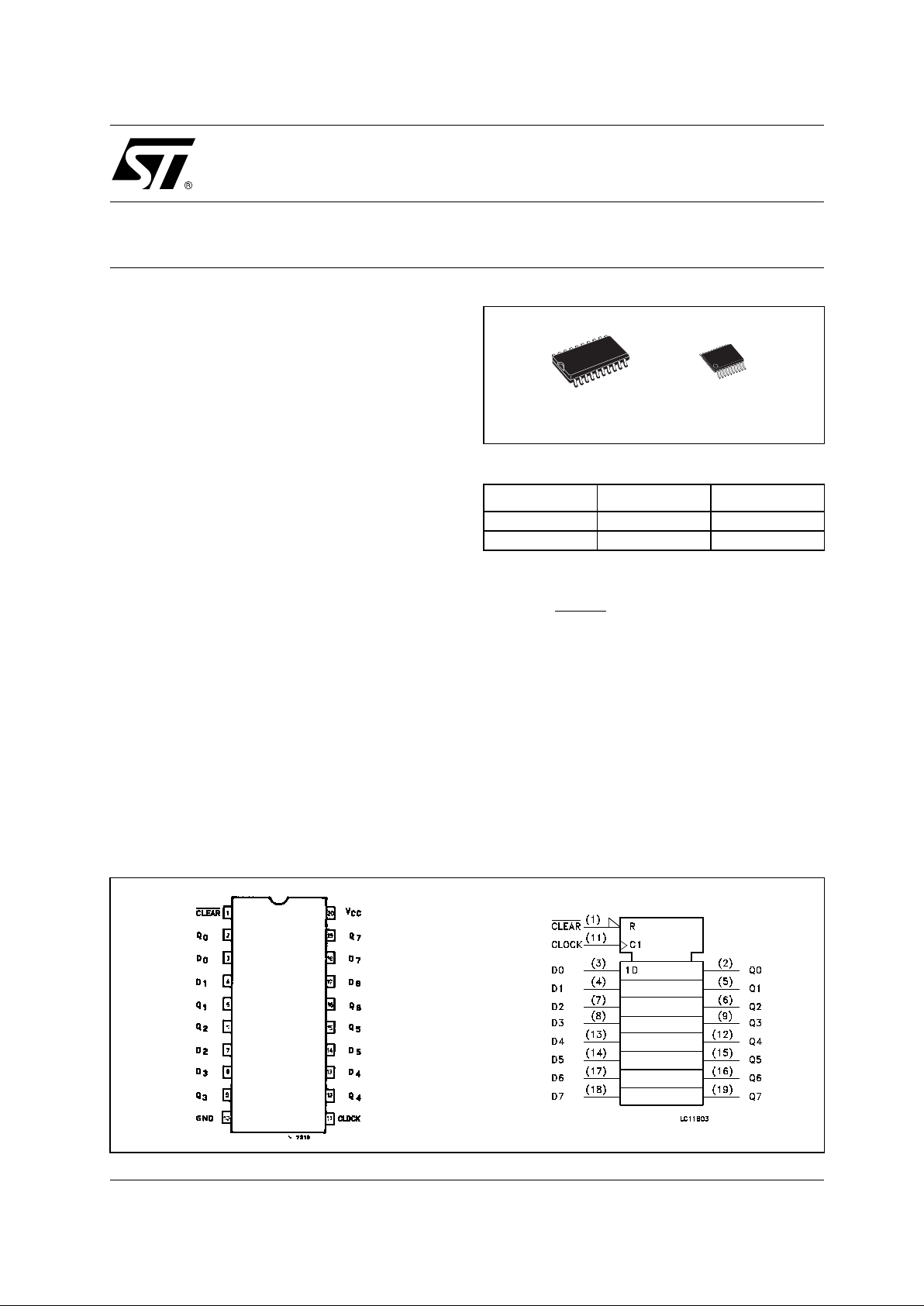
PIN CONNECTION AND IEC LOGIC SYMBOLS
ORDER CODES
PACKAGE TUBE T & R
SOP 74LVX273M 74LVX273MTR
TSSOP 74LVX273TTR
TSSOPSOP
Page 2
74LVX273
2/10
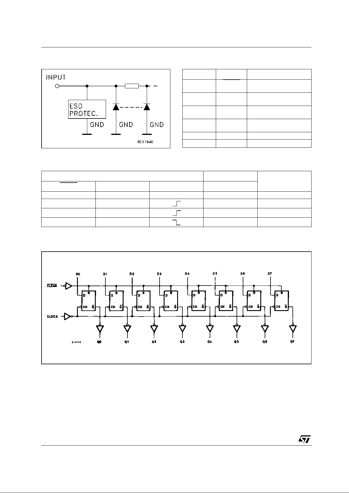
INPUT EQUIVALENT CIRCUIT PIN DESCRIPTION
TRUTH TABLE
X : Don’t Care
LOGIC DIAGRAM
This log i c diagram has not be used to esti m ate propagation delays
PIN No SYMBOL NAME AND FUNCTION
1 CLEAR
Asynchronous Master
Reset (Active LOW)
2, 5, 6, 9, 12,
15, 16,19
Q0 to Q7 Flip-Flop Outputs
3, 4, 7, 8, 13,
14, 17, 18
D0 to D7 Data Inputs
1 1 CLOCK Clock Input (LOW-to-HIGH
Edge Triggered)
10 GND Ground (0V)
20 V
CC
Positive Supply Voltage
INPUTS OUTPUT
FUNCTION
CLEAR
DBQ
L X X L CLEAR
HL L
HH H
HX
Q
n
NO CHANGE
Page 3
74LVX273
3/10
ABSOLUTE MAXIMUM RATINGS
Absolute Maximum Ratings are those values beyond which damage to the device may occur. Functional operation under these conditions is
not implied
RECOMMENDED OPERATING CONDITIONS
1) Truth T abl e guarante ed: 1.2V to 3.6 V
2) V
IN
from 0.8V to 2.0V
Symbol Parameter Value Unit
V
CC
Supply Voltage
-0.5 to +7.0 V
V
I
DC Input Voltage
-0.5 to +7.0 V
V
O
DC Output Voltage -0.5 to VCC + 0.5
V
I
IK
DC Input Diode Current
- 20 mA
I
OK
DC Output Diode Current
± 20 mA
I
O
DC Output Current
± 25 mA
I
CC
or I
GND
DC VCC or Ground Current
± 50 mA
T
stg
Storage Temperature
-65 to +150 °C
T
L
Lead Temperature (10 sec)
300 °C
Symbol Parameter Value Unit
V
CC
Supply Voltage (note 1)
2 to 3.6 V
V
I
Input Voltage
0 to 5.5 V
V
O
Output Voltage 0 to V
CC
V
T
op
Operating Temperature
-55 to 125 °C
dt/dv
Input Rise and Fall Time (note 2) (V
CC
= 3V)
0 to 100 ns/V
Page 4

74LVX273
4/10
DC SPECIFICATIONS
DYNAMIC SWITCHING CHARACTERISTICS
1) Worst c ase package .
2) Max number of outp ut s defined as (n). Data inp ut s are driven 0V to 3.3V, (n-1) outputs sw i tc hi ng and one output at GND.
3) Max number of data inputs (n) switching. (n-1) switching 0V to 3.3V. Inputs under test switching: 3.3V to threshold (V
ILD
), 0V to threshold
(V
IHD
), f=1MHz.
Symbol Parameter
Test Condition Value
Unit
V
CC
(V)
T
A
= 25°C
-40 to 85°C -55 to 125°C
Min. Typ. Max. Min. Max. Min. Max.
V
IH
High Level Input
Voltage
2.0 1.5 1.5 1.5
V3.0
2.0 2.0 2.0
3.6
2.4 2.4 2.4
V
IL
Low Level Input
Voltage
2.0 0.5 0.5 0.5
V3.0 0.8 0.8 0.8
3.6 0.8 0.8 0.8
V
OH
High Level Output
Voltage
2.0
IO=-50 µA
1.9 2.0 1.9 1.9
V3.0
I
O
=-50 µA
2.9 3.0 2.9 2.9
3.0
I
O
=-4 mA
2.58 2.48 2.4
V
OL
Low Level Output
Voltage
2.0
I
O
=50 µA
0.0 0.1 0.1 0.1
V3.0
I
O
=50 µA
0.0 0.1 0.1 0.1
3.0
I
O
=4 mA
0.36 0.44 0.55
I
I
Input Leakage
Current
3.6
V
I
= 5V or GND
± 0.1 ± 1 ± 1 µA
I
CC
Quiescent Supply
Current
3.6
V
I
= VCC or GND
44040µA
Symbol Parameter
Test Condition Value
Unit
V
CC
(V)
T
A
= 25°C
-40 to 85°C -55 to 125°C
Min. Typ. Max. Min. Max. Min. Max.
V
OLP
Dynamic Low
Voltage Quiet
Output (note 1, 2)
3.3
C
L
= 50 pF
0.3 0.8
V
V
OLV
-0.8 -0.3
V
IHD
Dynamic High
Voltage Input
(note 1, 3)
3.3 2.0
V
ILD
Dynamic Low
Voltage Input
(note 1, 3)
3.3 0.8
Page 5

74LVX273
5/10
AC ELECTRICAL CHARACTERISTICS (Input tr = tf = 3ns)
1) Skew is defined as the absolute value of the difference between the actual propagation delay for any two outputs of the same device switching in the same direction, either HIGH or LOW
2) Param eter guaranteed by design
(*) Vol tage range i s 3.3V ±
0.3V
CAPACITIVE CHARACTERISTICS
1) CPD is defined as the value of the IC’s internal equivalent capacitance which is calculated from the operating current consumption without
ad. (Refer to Test Circuit). Average operating current can be obtained by the following equation. I
CC(opr)
= CPD x VCC x fIN + ICC/8 (per circuit)
Symbol Parameter
Test Condition Value
Unit
V
CC
(V)
C
L
(pF)
T
A
= 25°C
-40 to 85°C -55 to 125°C
Min. Typ. Max. Min. Max. Min. Max.
t
PLH
t
PHL
Propagation Delay
Time
CK to Q
2.7
15 9.0 16.9 1.0 20.5 1.0 22.0
ns
2.7
50 11.5 20.4 1.0 24.0 1.0 25.5
3.3
(*)
15 7.1 11.0 1.0 13.0 1.0 14.5
3.3
(*)
50 9.6 14.5 1.0 16.5 1.0 18.0
t
PHL
Propagation Delay
Time
CLEAR
to Q
3.3
(*)
15 9.3 17.6 1.0 20.5 1.0 22.0
ns
3.3
(*)
50 11.8 21.1 1.0 24.0 1.0 25.5
5.0
(**)
15 7.3 11.5 1.0 13.5 1.0 15.5
5.0
(**)
50 9.8 15.0 1.0 17.0 1.0 18.0
t
W(L)
CLEAR pulse
Width, HIGH
2.7
50
5.0 6.0 6.0
ns
3.3
(*)
5.0 5.0 5.0
t
W
CLOCK pulse
Width, HIGH
2.7
50
5.5 6.5 6.5
ns
3.3
(*)
5.0 5.0 5.0
t
S
Setup Time Q to
CLOCK HIGH or
LOW
2.7
50
5.5 6.5 6.5
ns
3.3
(*)
4.5 4.5 4.5
t
h
Hold Time Q to
CLOCK HIGH or
LOW
2.7
50
1.0 1.0 1.0
ns
3.3
(*)
1.0 1.0 1.0
t
REM
Recovery Time
CLEAR
to Q
2.7
50
2.5 2.5 2.5
ns
3.3
(*)
2.0 2.0 2.0
f
MAX
Maximum Clock
Frequency
2.7 15 55 110 55 50
MHz
2.7 50 45 60 40 35
3.3
(*)
15 95 150 80 75
3.3
(*)
50 60 90 55 50
t
OSLH
t
OSHL
Output to Output
Skew Time (note
1,2)
2.7 50 0.5 1.0 1.5 1.5
ns
3.3
(*)
50 0.5 1.0 1.5 1.5
Symbol Parameter
Test Condition Value
Unit
V
CC
(V)
T
A
= 25°C
-40 to 85°C -55 to 125°C
Min. Typ. Max. Min. Max. Min. Max.
C
IN
Input Capacitance
3.3 5101010pF
C
PD
Power Dissipation
Capacitance
(note 1)
3.3
f
IN
= 10MHz
40 pF
Page 6

74LVX273
6/10
TEST CIRCUIT
CL =15/50pF or equivalent (i ncludes jig and probe cap acitance)
R
T
= Z
OUT
of pulse generator (typically 50Ω)
WAVEFORM 1 : PROPAGATION DELAYS, SETUP AND HOLD TIMES (f=1MHz; 50% duty cycle)
Page 7

74LVX273
7/10
WAVEFORM 2 : PROPAGATION DELAYS (f=1MHz; 50% duty cycle)
WAVEFORM 3 : RECOVERY TIME (f=1MHz; 50% duty cycle)
Page 8

74LVX273
8/10
DIM.
mm. inch
MIN. TYP MAX. MIN. TYP. MAX.
A 2.65 0.104
a1 0.1 0.2 0.004 0.008
a2 2.45 0.096
b 0.35 0.49 0.014 0.019
b1 0.23 0.32 0.009 0.012
C 0.5 0.020
c1 45° (typ.)
D 12.60 13.00 0.496 0.512
E 10.00 10.65 0.393 0.419
e 1.27 0.050
e3 11.43 0.450
F 7.40 7.60 0.291 0.300
L 0.50 1.27 0.020 0.050
M 0.75 0.029
S8° (max.)
SO-20 MECHANICAL DATA
PO13L
Page 9

74LVX273
9/10
DIM.
mm. inch
MIN. TYP MAX. MIN. TYP. MAX.
A 1.2 0.047
A1 0.05 0.15 0.002 0.004 0.006
A2 0.8 1 1.05 0.031 0.039 0.041
b 0.19 0.30 0.007 0.012
c 0.09 0.20 0.004 0.0089
D 6.4 6.5 6.6 0.252 0.256 0.260
E 6.2 6.4 6.6 0.244 0.252 0.260
E1 4.3 4.4 4.48 0.169 0.173 0.176
e 0.65 BSC 0.0256 BSC
K0° 8°0° 8°
L 0.45 0.60 0.75 0.018 0.024 0.030
TSSOP20 MECHANICAL DATA
c
E
b
A2
A
E1
D
1
PIN 1 IDENTIFICATION
A1
L
K
e
0087225C
Page 10

74LVX273
10/10
Information furnished is bel ieved to be accurate and reliable. However, STMicroe lectronics assumes no responsibility for the
consequences of use of such information nor for any infringement of patents or other rights of third parties which may result from
its use. No li cense is granted by i mp lication or otherwise under a ny patent or patent rig hts of STMicroelectronics. S pec ificat ions
mentioned in this publication ar e subject to change without notice. This publication supersedes and replaces all information
previously supplied. S TMicroelectronics products are not authorized for use as critica l components in life suppo rt devices or
systems without express written approval of STMicroelectronics.
© The ST logo is a registered trademark of STMicroelectronics
© 2001 STM icroelectronics - P rinted in Italy - All Righ ts Reserved
STMicr o el ectronics GROUP OF COMPA NI E S
Australi a - Brazil - Chi na - Finlan d - F rance - Germ any - Hong Kon g - India - Italy - Japan - Malaysia - Mal ta - Morocco
Singapo re - Spain - Sweden - Swit zerland - Un i ted Kingdom
© http://www.st.com
 Loading...