

Page 1
74LVX244
Low Voltage Octal Buffer/Line Driver with
3-STATE Outputs
74LVX244 Low Voltage Octal Buffer/Line Driver with 3-STATE Outputs
February 1993
Revised March 1999
General Description
The LVX244 is an octal non-i nver ting bu ffer an d line driv er
designed to be employed as a memory address driver,
clock driver and bus or iented transmitter or receive r which
provides improved PC board density. The inputs tolerate
up to 7V allowing interface of 5V systems to 3V systems.
Features
■ Input voltage translation from 5V to 3V
■ Ideal for low power/low noise 3.3V applications
■ Guaranteed simultaneous switching noise level and
dynamic threshold performance
Ordering Code:
Order Number Package Number Package Description
74LVX244M M20B 20-Lead Small Outline Integrated Circuit (SOIC), JEDEC MS-013, 0.300” Wide
74LVX244SJ M20D 20-Lead Small Outline Package (SOP), EIAJ TYPE II, 5.3mm Wide
74LVX244MTC MTC20 20-Lead Thin Shrink Small Outline Package (TSSOP), JEDEC MO-153, 4.4mm Wide
Devices also availab le in Tape and Reel. Specify by appending suffix letter “X” to the ord ering code.
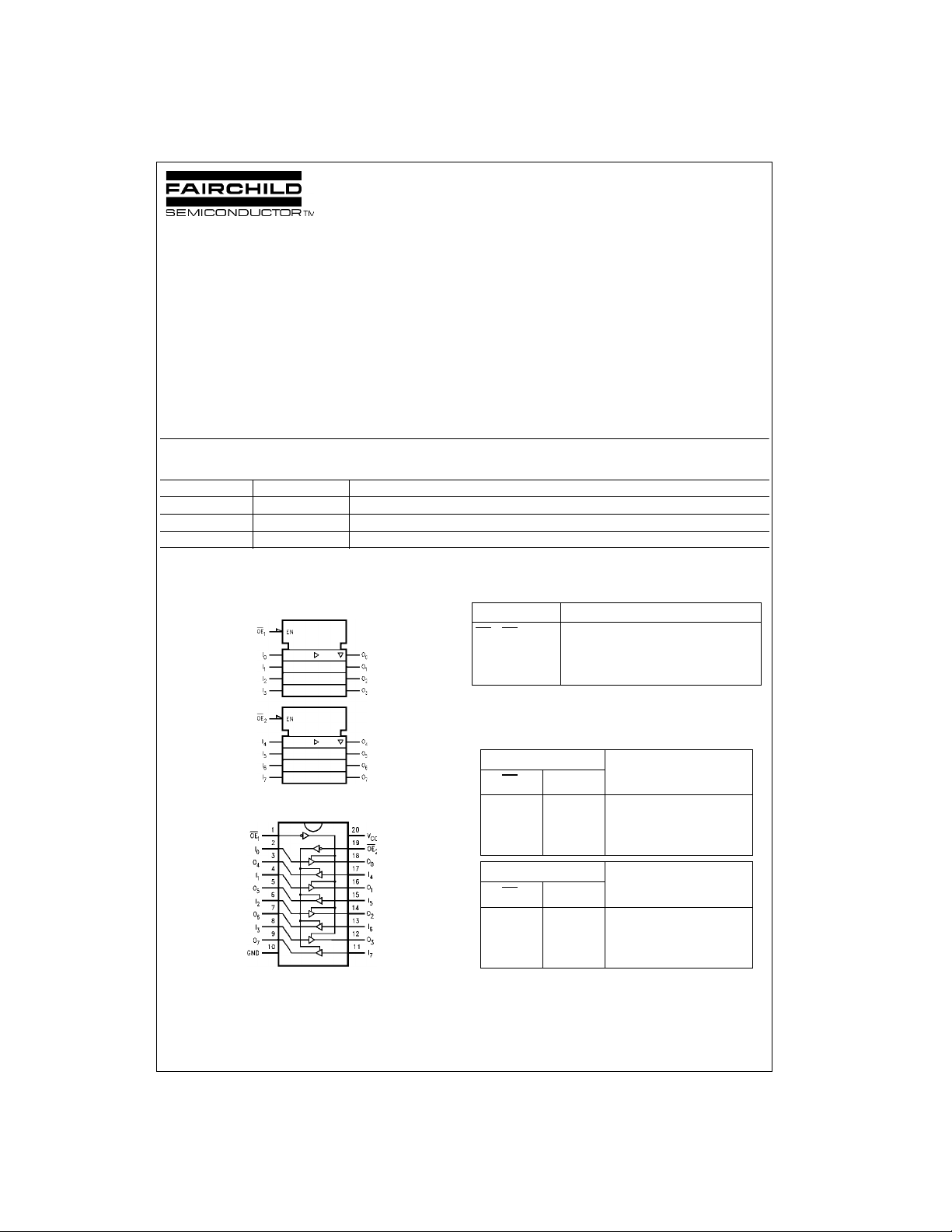
Logic Symbol
IEEE/IEC
Pin Descriptions
Pin Names Description
OE
I
0–I7
O
1
0–O7
, OE
3-STATE Output Enable Inputs
2
Inputs
Outputs
Truth Ta bles
Inputs Outputs
I
n
Inputs Outputs
I
n
(Pins 12, 14, 16, 18)
(Pins 3, 5, 7, 9)
Connection Diagram
OE
1
LL L
LH H
HX Z
OE
2
LL L
LH H
HX Z
H = HIGH Voltage Level L = LOW Voltage Level
X = Immaterial Z = High Impedance
© 1999 Fairchild Semiconductor Corporation DS011552.prf www.fairchildsemi.com
Page 2
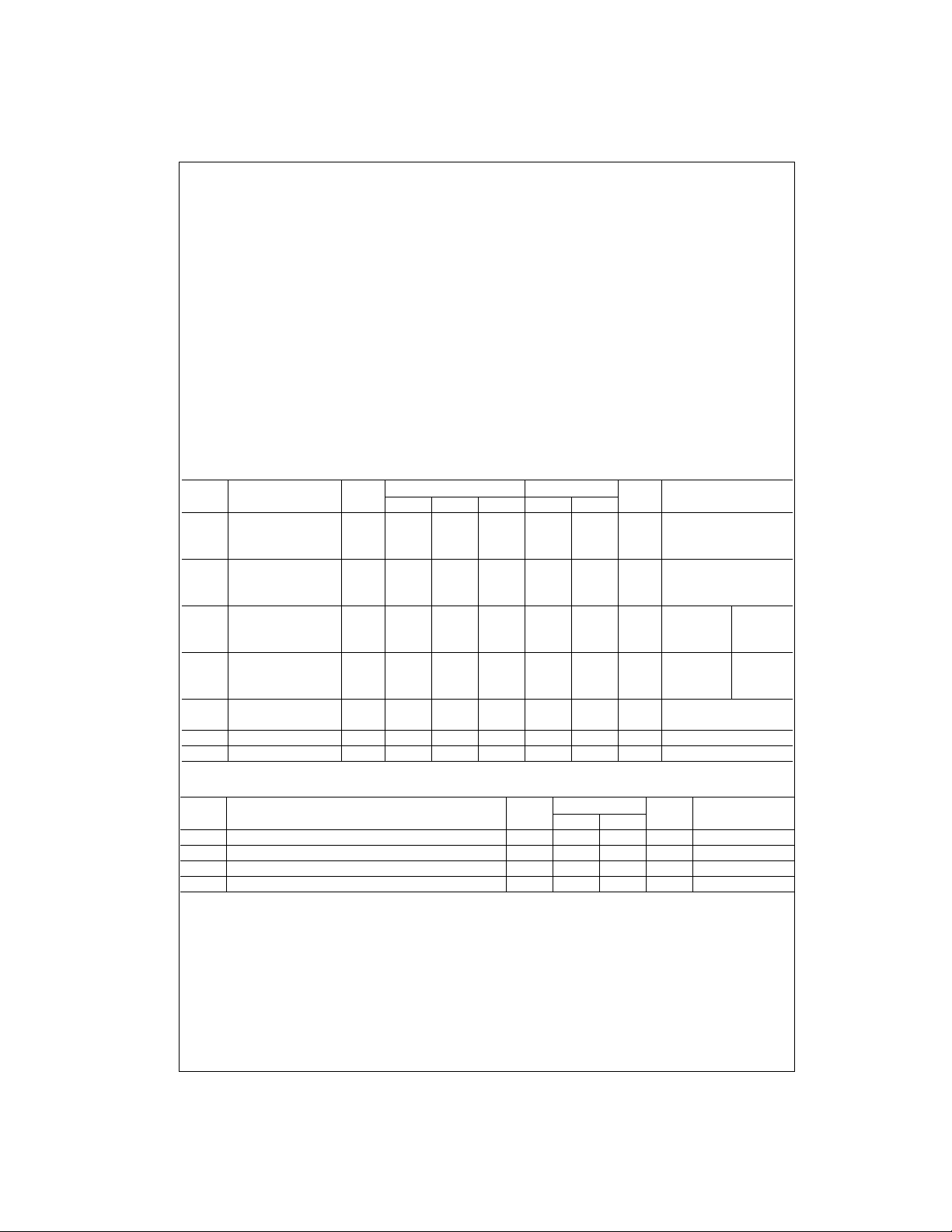
Absolute Maximum Ratings(Note 1) Recommended Operating
Supply Voltage (VCC) −0.5V to +7.0V
DC Input Diode Current (I
74LVX244
= −0.5V −20 mA
V
I
DC Input Voltage (V
DC Output Diode Current (I
= −0.5V −20 mA
V
O
= VCC + 0.5V +20 mA
V
O
DC Output Voltage (V
)
IK
) −0.5V to 7V
I
)
OK
) −0.5V to VCC + 0.5V
O
DC Output Source
or Sink Current (I
or Ground Current
DC V
CC
or I
(I
CC
GND
Storage Temperature (T
) ±25 mA
O
) ±75 mA
) −65°C to +150°C
STG
Power Dissipation 180 mW
Conditions
Supply Voltage (V
Input Voltage (V
Output Voltage (V
Operating Temperature (TA) −40°C to +85°C
Input Rise and Fall Time (∆t/∆V) 0 ns/V to 100 ns/V
Note 1: The “Absolute Maximum Ratin gs” are those v alues beyon d which
the safety of the dev ice cannot be guaranteed. T he device sh ould not be
operated at these limits. The parametric values defined in the Electrical
Characteristics tables are not guaranteed at the absolute maximum ratings.
The “Recommend ed O peratin g Cond itions” t able w ill defin e the c ondit ions
for actual device operation.
Note 2: Unused inputs must be held HIGH or LOW. They may not float.
(Note 2)
) 2.0V to 3.6V
CC
)0V to 5.5V
I
) 0V to V
o
DC Electrical Characteristics
Symbol Parameter
V
HIGH Level Input 2.0 1.5 1.5
IH
Voltage 3.0 2.0 2.0 V
V
LOW Level Input 2.0 0.5 0.5
IL
Voltage 3.0 0.8 0.8 V
V
HIGH Level Output 2.0 1.9 2.0 1.9 VIN = VIH or VILIOH = −50 µA
OH
Voltage 3.0 2.9 3.0 2.9 V IOH = −50 µA
V
LOW Level Output 2.0 0.0 0.1 0.1 VIN = VIH or VILIOL = 50 µA
OL
Voltage 3.0 0.0 0.1 0.1 V IOL = 50 µA
I
3-STATE Output 3.6 ±0.25 ±2.5 µAVIN = VIH or V
OZ
Off-State Current V
I
Input Leakage Current 3.6 ±0.1 ±1.0 µAVIN = 5.5V or GND
IN
I
Quiescent Supply Current 3.6 4.0 40.0 µAVIN = VCC or GND
CC
V
CC
3.6 2.4 2.4
3.6 0.8 0.8
3.0 2.58 2.48 IOH = −4 mA
3.0 0.36 0.44 IOL = 4 mA
TA = +25°CT
Min Typ Max Min Max
= −40°C to +85°C
A
Units Conditions
= VCC or GND
OUT
CC
IL
Noise Characteristics
Symbol Parameter
V
Quiet Output Maximum Dynamic V
OLP
V
Quiet Output Minimum Dynamic V
OLV
V
Minimum HIGH Level Dynamic Input Voltage 3.3 2.0 V 50
IHD
V
Maximum LOW Level Dynamic Input Voltage 3.3 0.8 V 50
ILD
Note 3: Input tr = tf = 3 ns
(Note 3)
OL
OL
www.fairchildsemi.com 2
V
CC
(V)
3.3 0.5 0.8 V 50
3.3 −0.5 −0.8 V 50
TA = 25°C
Typ Limit
Units
CL (pF)
Page 3
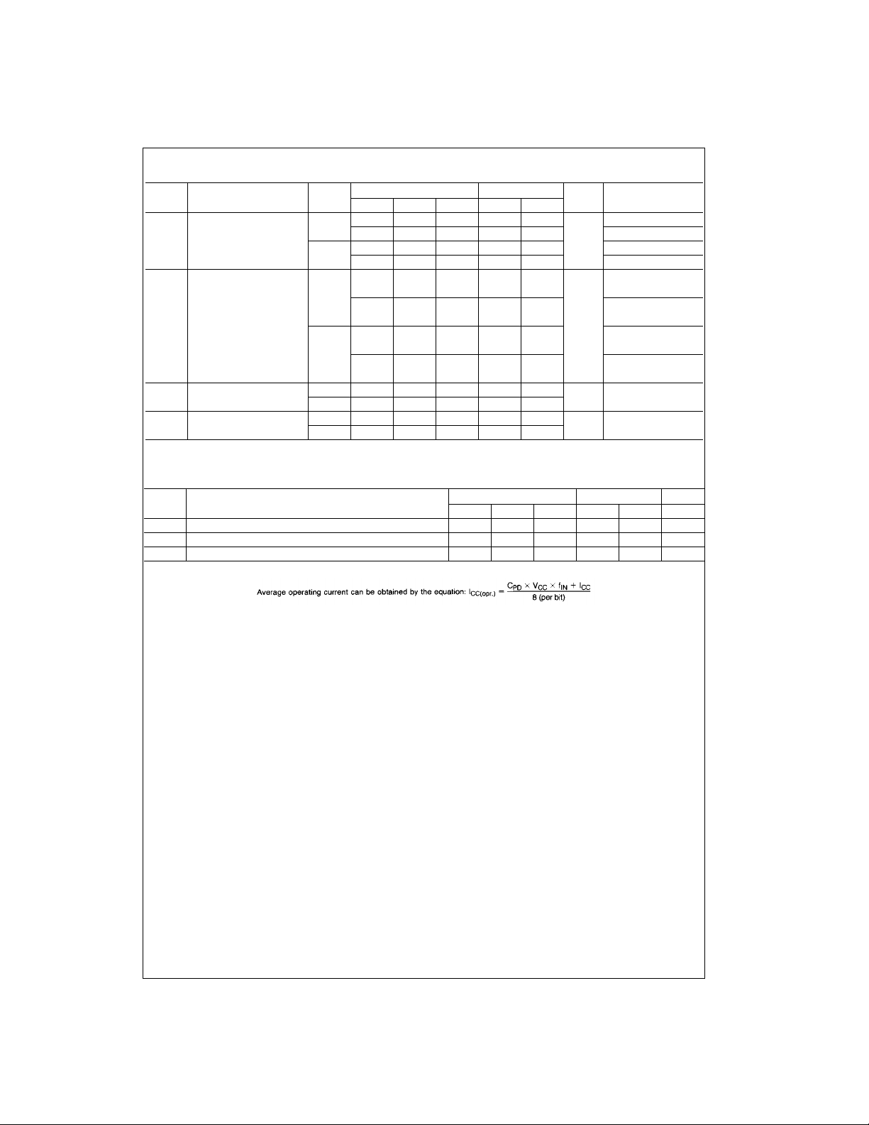
AC Electrical Characteristics
V
Symbol Parameter
t
Propagation Delay 2.7 6.1 11.4 1.0 13.5
PLH
t
Time 8.614.91.017.0 CL = 50 pF
PHL
(V)
CC
TA = +25°CT
Min Typ Max Min Max
3.3 ± 0.3 4.7 7.1 1.0 8.5 CL = 15 pF
7.210.61.012.0 CL = 50 pF
t
3-STATE Output 2.7 7.1 13.8 1.0 16.5
PZL
t
Enable Time RL = 1 kΩ
PZH
9.617.31.020.0 CL = 50 pF,
3.3 ± 0.3 5.5 8.8 1.0 10.5 CL = 15 pF,
8.012.31.014.0 CL = 50 pF,
t
3-STATE Output 2.7 11.6 16.0 1.0 19.0
PLZ
t
Disable Time 3.3 ± 0.3 9.7 11.4 1.0 13.0 RL = 1 kΩ
PHZ
t
Output to Output 2.7 1.5 1.5
OSLH
t
Skew (Note 4) 3.3 1.5 1.5
OSHL
Note 4: Parameter gu aranteed by design. t
OSLH
= |t
PLHm
− t
|, t
= |t
PLHn
OSHL
PHLm
− t
PHLn
|
= −40°C to +85°C
A
Units Conditions
CL = 15 pF
ns
CL = 15 pF,
RL = 1 kΩ
ns
RL = 1 kΩ
RL = 1 kΩ
CL = 50 pF,
ns
CL = 50 pF
ns
Capacitance
Symbol Parameter
C
Input Capacitance 4 10 10 pF
IN
C
Output Capacitance 6 pF
OUT
C
Power Dissipation Capacitance (Note 5) 19 pF
PD
Note 5: CPD is defined as the value of the internal equiv alent capacitance w hic h is calculated from th e operating current cons umption without loa d.
TA = +25°CT
Min Typ Max Min Max
=−40°C to +85°C
A
74LVX244
Units
3 www.fairchildsemi.com
Page 4
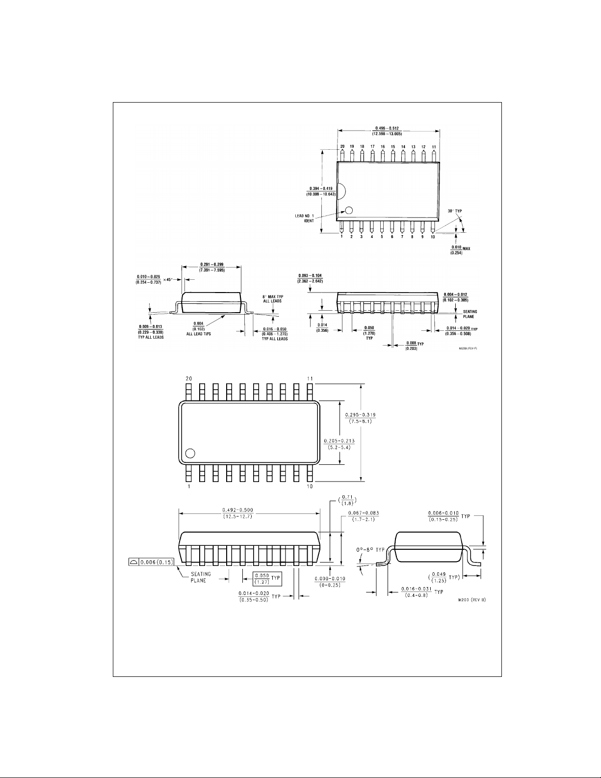
Physical Dimensions inches (millimeters) unless otherwise noted
74LVX244
20-Lead Small Outline Integrated Circuit (SOIC), JEDEC MS-013, 0.300” Wide
20-Lead Small Outline Package ( SOP), EIAJ TYPE II, 5.3mm Wide
Package Number M20B
Package Number M20D
www.fairchildsemi.com 4
Page 5
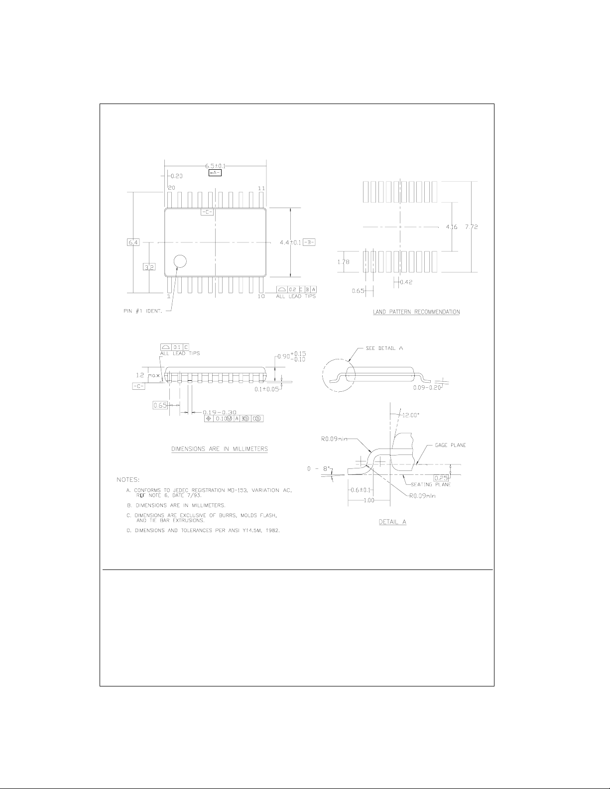
Physical Dimensions inches (millimeters) unless otherwise noted (Continued)
74LVX244 Low Voltage Octal Buffer/Line Driver with 3-STATE Outputs
20-Lead Thin Shrink Small Outline Package (TSSOP), JEDEC MO-153, 4.4mm Wide
LIFE SUPPORT POLICY
FAIRCHILD’S PRODUCTS ARE NOT AUTHORIZED FOR USE AS CRITICAL COMPONENTS IN LIFE SUPPORT
DEVICES OR SYSTEMS WITHOUT THE EXPRESS WRITTEN APPROVAL OF THE PRESIDENT OF FAIRCHILD
SEMICONDUCTOR CORPORATION. As used herein:
1. Life support devices or systems are devices or systems
which, (a) are intended for surgical implant into the
body, or (b) support or sustain life, and (c) whose failure
to perform when properly used in accordance with
instructions for use provide d in the labe l ing, can be re asonably expected to result in a significant injury to the
user.
Fairchild does not assume any responsibility for use of any circuitry described, no circuit patent licenses are implied and Fairchild reserves the right at any time without notice to change said circuitry and specifications.
Package Number MTC20
2. A critical componen t in any com ponen t of a life s upport
device or system whose failu re to perform can b e reasonably expected to cause the failure of the l ife s upp or t
device or system, or to affect its safety or effectiveness.
www.fairchildsemi.com
 Loading...