

Datasheet 74LVX157SJX, 74LVX157SJ, 74LVX157MX, 74LVX157MTCX, 74LVX157MTC Datasheet (Fairchild Semiconductor)
...Page 1
May 1993
Revised March 1999
74LVX157 Low Voltage Quad 2-Input Multiplexer
© 1999 Fairchild Semiconductor Corporation DS011608.prf www.fairchildsemi.com
74LVX157
Low Voltage Quad 2-Input Multiplexer
General Description
The LVX157 is a high-speed quad 2-input multiplexer. Four
bits of data from two sources can be selected using the
common Select and Enable inputs. The four outputs
present the selected data in the true (noninverted) form.
The LVX157 can also be used as a function gener ator.
Features
■ Input voltage level translation from 5V to 3V
■ Ideal for low power/low noise 3.3V applications
■ Guaranteed simultaneous switching noise level and
dynamic threshold performance
Ordering Code:
Devices are also avai lable in Tape and Reel. Specify by append ing letter suffix “X” to the ordering code.
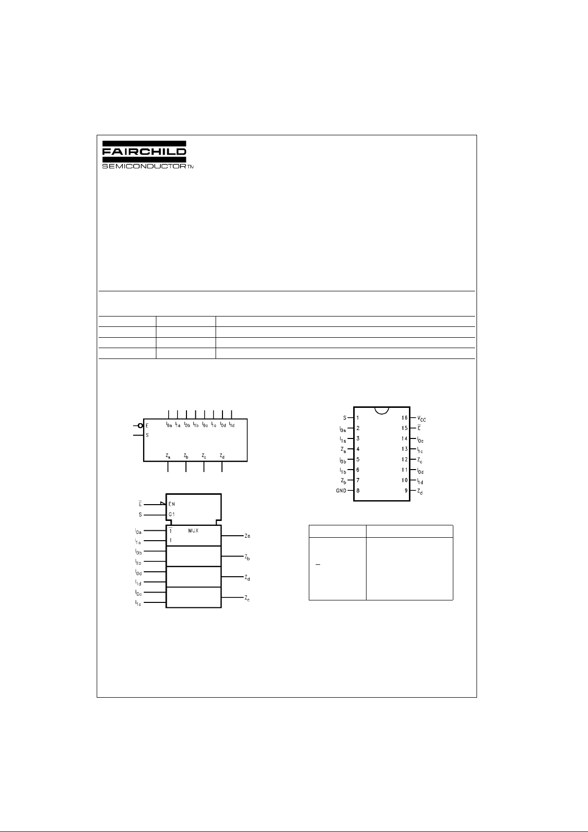
Logic Symbols
IEEE/IEC
Connection Diagram
Pin Descriptions
Order Number Package Number Package Description
74LVX157M M16A 16-Lead Small Outline Integrated Circuit (SOIC), JEDEC MS-012, 0.150” Narrow
74LVX157SJ M16D 16-Lead Small Outline Package (SOP), EIAJ TYPE II, 5.3mm Wide
74LVX157MTC MTC16 16-Lead Thin Shrink Small Outline Package (TSSOP), JEDEC MO-153, 4.4mm Wide
Pin Names Description
I
0a–I0d
Source 0 Data Inputs
I
1a–I1d
Source 1 Data Inputs
E
Enable Input
S Select Input
Z
a–Zd
Outputs
Page 2
www.fairchildsemi.com 2
74LVX157
Truth Table
H = HIGH Voltage Level
L = LOW Voltage Level
X = Immaterial
Functional Description
The LVX157 is a quad 2-input multiplexer. It selects four
bits of data from two sources un der the control of a common Select input (S). The Enable input (E
) is active-LOW.
When E
is HIGH, all of the outputs (Z) are forced LOW
regardless of all other inputs. The LVX157 is the logic
implementation of a 4-pole, 2-position switch where the
position of the switch is determined by the logic levels supplied to the Select input. The logic equations for the outputs
are shown below:
Z
a
= E • (I1a • S + I0a • S)
Z
b
= E • (I
1b
• S + I0b • S)
Z
c
= E • (I
1c
• S + I0c • S)
Z
d
= E • (I
1d
• S + I0d • S)
A common use of the LVX157 is the moving of data from
two groups of registers to four common output busses. The
particular register from which the data comes is determined
by the state of t he S elect in put . A less ob vious us e is as a
function generator. The LVX157 can generate any four of
the sixteen different functions of two variables with one
variable common. This is useful for implementing gating
functions.
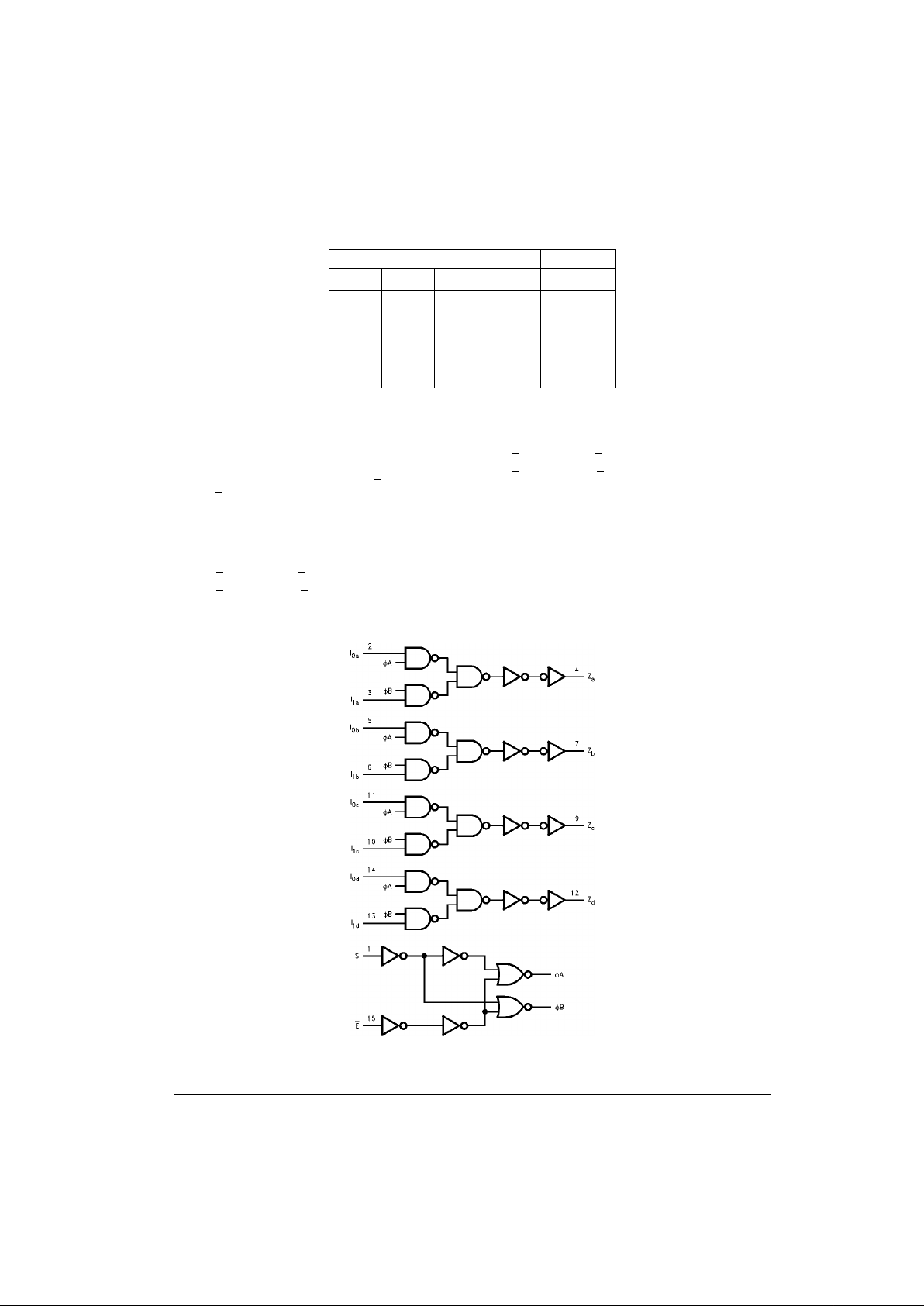
Logic Diagram
Inputs Outputs
E
SI0I
1
Z
HXXX L
LHXL L
LHXH H
LLLX L
LLHX H
Page 3

3 www.fairchildsemi.com
74LVX157
Absolute Maximum Ratings(Note 1) Recommended Operating
Conditions
(Note 2)
Note 1: The “Absolute Maximum Ratings ” are those val ues beyond w hich
the safety of the device cannot be guaranteed. The device should not be
operated at these limits. The parametric values defined in the Electrical
Characteristics tables are not guaranteed at the absolute maximum ratings.
The “Recommend ed O peratin g Cond itions” t able w ill defin e the condition s
for actual device operation.
Note 2: Unused inputs must be held HIGH or LOW. They may not float.
DC Electrical Characteristics
Noise Characteristics
(Note 3)
Note 3: Input tr = tf = 3ns
Supply Voltage (VCC) −0.5V to +7.0V
DC Input Diode Current (I
IK
)
V
I
= −0.5V −20 mA
DC Input Voltage (V
I
) −0.5V to 7V
DC Output Diode Current (I
OK
)
V
O
= −0.5V −20 mA
V
O
= VCC + 0.5V +20 mA
DC Output Voltage (V
O
) −0.5V to VCC + 0.5V
DC Output Source
or Sink Current (I
O
) ±25 mA
DC V
CC
or Ground Current
(I
CC
or I
GND
) ±50 mA
Storage Temperature (T
STG
) −65°C to +150°C
Power Dissipation 180 mW
Supply Voltage (V
CC
) 2.0V to 3.6V
Input Voltage (V
I
) 0V to 5.5V
Output Voltage (V
O
)0V to V
CC
Operating Temperature (TA) −40°C to +85°C
Input Rise and Fall Time (∆t/∆V) 0 ns/V to 100 ns/V
Symbol Parameter
V
CC
TA = +25°C TA = −40°C to +85°C
Units Conditions
Min Typ Max Min Max
V
IH
HIGH Level 2.0 1.5 1.5
Input Voltage 3.0 2.0 2.0 V
3.6 2.4 2.4
V
IL
LOW Level 2.0 0.5 0.5
Input Voltage 3.0 0.8 0.8 V
3.6 0.8 0.8
V
OH
HIGH Level 2.0 1.9 2.0 1.9 VIN = VIL or VIHIOH = −50 µA
Output Voltage 3.0 2.9 3.0 2.9 V IOH = −50 µA
3.0 2.58 2.48 IOH = −4 mA
V
OL
LOW Level 2.0 0.0 0.1 0.1 VIN = V
IL
or VIHIOL = 50 µA
Output Voltage 3.0 0.0 0.1 0.1 V IOL = 50 µA
3.0 0.36 0.44 IOL = 4 mA
I
IN
Input Leakage Current 3.6 ±0.1 ±1.0 µAVIN = 5.5V or GND
I
CC
Quiescent Supply Current 3.6 4.0 40.0 µAVIN = VCC or GND
Symbol Parameter
V
CC
(V)
TA = 25°C
Units
CL (pF)
Typ Limit
V
OLP
Quiet Output Maximum Dynamic V
OL
3.3 0.3 0.5 V 50
V
OLV
Quiet Output Minimum Dynamic V
OL
3.3 −0.3 −0.5 V 50
V
IHD
Minimum HIGH Level Dynamic Input Voltage 3.3 2.0 V 50
V
ILD
Maximum LOW Level Dynamic Input Voltage 3.3 0.8 V 50
Page 4

www.fairchildsemi.com 4
74LVX157
AC Electrical Characteristics
Note 4: Paramete r guaranteed by desig n.
t
OSLH
= |t
PLHm
− t
PLHn
|.
t
OSHL
= |t
PHLm
− t
PHLn
|.
Capacitance
Note 5: CPD is defined as the value of the internal equivalent capacitance whic h is calculated from the operating current cons umption without load.
Average operating cu rrent can be obtained b y the equation: I
CC(opr.)
= CPD × V
CC
× fIN + I
CC
Symbol Parameter
V
CC
(V)
TA = +25°C TA = −40°C to +85°C
Units
CL (pF)
Min Typ Max Min Max
t
PLH
Propagation 2.7 6.6 12.5 1.0 15.5
ns
15
t
PHL
Delay Time 9.1 16.0 1.0 19.0 50
I n to Z
n
3.3 ± 0.3 5.1 7.9 1.0 9.5 15
7.6 11.4 1.0 13.0 50
t
PLH
Propagation 2.7 8.9 16.9 1.0 20.5
ns
15
t
PHL
Delay Time 11.4 20.4 1.0 24.0 50
S to Z
n
3.3 ± 0.3 7.0 11.0 1.0 13.0 15
9.5 14.5 1.0 16.5 50
t
PLH
t
PHL
Propagation 2.7 9.1 17.6 1.0 20.5
ns
15
Delay Time 11.6 21.1 1.0 24.0 50
E to Z
n
3.3 ± 0.3 7.2 11.5 1.0 13.5 15
9.7 15.0 1.0 17.0 50
t
OSHL
Output to Output 2.7 1.5 1.5
ns
50
t
OSLH
Skew (Note 4) 3.3 1.5 1.5
Symbol Parameter
TA = +25°C TA = −40°C to +85°C
Units
Min Typ Max Min Max
C
IN
Input Capacitance 4 10 10 pF
C
PD
Power Dissipation Capacitance (Note 5) 20 pF
Page 5

5 www.fairchildsemi.com
74LVX157
Physical Dimensions inches (millimeters) unless otherwise noted
16-Lead Small Outline Integrated Circuit (SOIC), JEDEC MS-012, 0.150” Narrow
Package Number M16A
16-Lead Small Outline Package (SOP), EIAJ TYPE II, 5.3mm Wide
Package Number M16D
Page 6

Fairchild does not assume any responsibility for use of any circuitry described, no circuit patent licenses are implied and Fairchild reserves the right at any time without notice to change said circuitry and specifications.
74LVX157 Low Voltage Quad 2-Input Multiplexer
LIFE SUPPORT POLICY
FAIRCHILD’S PRODUCTS ARE NOT AUTHORIZED FOR USE AS CRITICAL COMPONENTS IN LIFE SUPPORT
DEVICES OR SYSTEMS WITHOUT THE EXPRESS WRITTEN APPROVAL OF THE PRESIDENT OF FAIRCHILD
SEMICONDUCTOR CORPORATION. As used herein:
1. Life support devices or systems are devices or syste ms
which, (a) are intended for surgical implant into the
body, or (b) support or sustain life, and (c) whose failure
to perform when properly used in accordance with
instructions for use provided in the labeling, can be reasonably expected to result in a significant inju ry to the
user.
2. A critical component i n any compon ent of a lif e support
device or system whose failu re to perform can be reasonably expected to ca use the fa i lure of the life su pp ort
device or system, or to affect its safety or effectiveness.
www.fairchildsemi.com
Physical Dimensions inches (millimeters) unless otherwise noted (Continued)
16-Lead Thin Shrink Small Outline Package (TSSOP), JEDEC MO-153, 4.4mm Wide
Package Number MTC16
 Loading...