

Page 1
INTEGRATED CIRCUITS
74LVU04
Hex inverter
Product specification
Supersedes data of 1997 Feb 12
IC24 Data Handbook
1998 Apr 20
Page 2
Philips Semiconductors Product specification
74L VU04Hex inverter
FEA TURES
•Wide operating voltage: 1.0 to 5.5 V
•Optimized for Low Voltage applications: 1.0 to 3.6 V
•Accepts TTL input levels between V
•Typical V
T
amb
•Typical V
T
amb
(output ground bounce) < 0.8 V at VCC = 3.3 V,
OLP
= 25°C.
(output VOH undershoot) > 2 V at VCC = 3.3 V,
OHV
= 25°C.
= 2.7 V and VCC = 3.6 V
CC
•Output capability: standard
•I
category: SSI
CC
QUICK REFERENCE DATA
GND = 0 V; T
SYMBOL
t
NOTES:
1. C
is used to determine the dynamic power dissipation (PD in µW)
PD
= CPD V
P
D
f
= input frequency in MHz; CL = output load capacitance in pF;
i
= output frequency in MHz; VCC = supply voltage in V;
f
o
(C
L
2. The condition is V
= 25°C; tr = tf 2.5 ns
amb
PHL/tPLH
C
I
C
PD
CC
2
V
fo) = sum of the outputs.
CC
PARAMETER CONDITIONS TYPICAL UNIT
Propagation delay
nA to nY
Input capacitance 3.5 pF
Power dissipation capacitance per gate Notes 1, 2 18 pF
2
fi (CL V
= GND to V
I
CC.
2
fo) where:
CC
DESCRIPTION
The 74LVU04 is a low-voltage, Si-gate CMOS device and is pin
compatible with the 74HCU04.
The 74LVU04 is a general purpose hex inverter. Each of the six
inverters is a single stage with unbuffered outputs.
CL = 15 pF;
VCC = 3.3 V
6 ns
ORDERING INFORMATION
PACKAGES TEMPERATURE RANGE OUTSIDE NORTH AMERICA NORTH AMERICA PKG. DWG. #
14-Pin Plastic DIL –40°C to +125°C 74LVU04 N 74LVU04 N SOT27-1
14-Pin Plastic SO –40°C to +125°C 74LVU04 D 74LVU04 D SOT108-1
14-Pin Plastic SSOP Type II –40°C to +125°C 74LVU04 DB 74LVU04 DB SOT337-1
14-Pin Plastic TSSOP Type I –40°C to +125°C 74LVU04 PW 74LVU04PW DH SOT402-1
PIN DESCRIPTION
PIN NUMBER SYMBOL NAME AND FUNCTION
1, 3, 5, 9, 11, 13 1A – 6A Data inputs
2, 4, 6, 8, 10, 12 1Y – 6Y Data outputs
7 GND Ground (0 V)
14 V
CC
Positive supply voltage
FUNCTION TABLE
INPUTS OUTPUTS
nA nY
L H
H L
NOTES:
H = HIGH voltage level
L = LOW voltage level
1998 Apr 20 853–1918 19257
2
Page 3

Philips Semiconductors Product specification
Hex inverter
PIN CONFIGURATION
1
1A
2
1Y
3
2A
4
2Y
5
3A
6
3Y
GND
7
LOGIC SYMBOL (IEEE/IEC)
12
34
56
1
1
1
14
V
13
6A
12
6Y
11
5A
10
5Y
9
4A
8
4Y
SV00396
CC
74LVU04
LOGIC SYMBOL
2Y
6Y
SV00397
V
CCVCC
2
4
6
8
10
12
1A 1Y
1
2A
3
5
3A 3Y
4A 4Y
9
11
5A 5Y
6A
13
SCHEMATIC DIAGRAM (ONE INVERTER)
V
CC
98
11 10
13 12
1
1
1
SV00398
100
nA nY
170
SV00400
RECOMMENDED OPERATING CONDITIONS
SYMBOL PARAMETER CONDITIONS MIN TYP. MAX UNIT
V
V
V
T
amb
tr, t
NOTE:
1. The LV is guaranteed to function down to V
DC supply voltage See Note1 1.0 3.3 5.5 V
CC
Input voltage 0 – V
I
Output voltage 0 – V
O
Operating ambient temperature range in free air
Input rise and fall times
f
CC
See DC and AC
characteristics
VCC = 1.0V to 2.0V
VCC = 2.0V to 2.7V
VCC = 2.7V to 3.6V
VCC = 3.6V to 5.5V
= 1.0V (input levels GND or VCC); DC characteristics are guaranteed from VCC = 1.2V to VCC = 5.5V.
–40
–40
–
–
–
–
–
–
–
–
CC
CC
+85
+125
500
200
100
50
ns/V
V
V
°C
1998 Apr 20
3
Page 4
Philips Semiconductors Product specification
V
V
V
V
voltage
V
V
voltage
Hex inverter
ABSOLUTE MAXIMUM RATINGS
1, 2
74LVU04
In accordance with the Absolute Maximum Rating System (IEC 134).
Voltages are referenced to GND (ground = 0V).
SYMBOL
V
CC
I
IK
I
OK
I
O
I
GND
I
CC
T
stg
P
TOT
DC supply voltage –0.5 to +7.0 V
DC input diode current VI < –0.5 or VI > VCC + 0.5V 20 mA
DC output diode current VO < –0.5 or VO > VCC + 0.5V 50 mA
DC output source or sink current
– standard outputs
DC VCC or GND current for types with
,
– standard outputs 50
Storage temperature range –65 to +150 °C
Power dissipation per package
– plastic DIL
– plastic mini-pack (SO)
– plastic shrink mini-pack (SSOP and TSSOP)
PARAMETER CONDITIONS RATING UNIT
–0.5V < VO < VCC + 0.5V
25
mA
mA
for temperature range: –40 to +125°C
above +70°C derate linearly with 12 mW/K
above +70°C derate linearly with 8 mW/K
above +60°C derate linearly with 5.5 mW/K
750
500
400
mW
NOTE:
1. Stresses beyond those listed may cause permanent damage to the device. These are stress ratings only and functional operation of the
device at these or any other conditions beyond those indicated under “recommended operating conditions” is not implied. Exposure to
absolute-maximum-rated conditions for extended periods may affect device reliability .
2. The input and output voltage ratings may be exceeded if the input and output current ratings are observed.
DC ELECTRICAL CHARACTERISTICS
Over recommended operating conditions. V oltages are referenced to GND (ground = 0V).
SYMBOL P ARAMETER TEST CONDITIONS
VCC = 1.2V 1.0 1.0
IH
HIGH level Input
voltage
VCC = 2.0V 1.6 1.6
VCC = 2.7 to 3.6V 2.4 2.4
VCC = 4.5 to 5.5V 0.8V
VCC = 1.2V 0.2 0.2
IL
LOW level Input
voltage
VCC = 2.0V 0.4 0.4
VCC = 2.7 to 3.6V 0.5 0.5
VCC = 4.5 to 5.5 0.2V
VCC = 1.2V; VI = VIH or V
VCC = 2.0V; VI = VIH or V
OH
HIGH level output
VCC = 2.7V; VI = VIH or V
V
VCC = 3.0V; VI = VIH or V
VCC = 4.5V;VI = VIH or V
OH
HIGH level output
voltage
VCC = 3.0V;VI = VIH or V
VCC = 4.5V;VI = VIH or V
VCC = 1.2V; VI = VIH or V
VCC = 2.0V; VI = VIH or V
OL
LOW level output
VCC = 2.7V; VI = VIH or V
V
VCC = 3.0V;VI = VIH or V
VCC = 4.5V;VI = VIH or V
–IO = 100µA 1.2
IL;
–IO = 100µA 1.8 2.0 1.8
IL;
–IO = 100µA 2.5 2.7 2.5
IL;
–IO = 100µA 2.8 3.0 2.8
IL;
–IO = 100µA 4.3 4.5 4.3
IL;
–IO = 6mA 2.40 2.82 2.20
IL;
–IO = 12mA 3.60 4.20 3.50
IL;
IO = 100µA 0
IL;
IO = 100µA 0 0.2 0.2
IL;
IO = 100µA 0 0.2 0.2
IL;
IO = 100µA 0 0.2 0.2
IL;
IO = 100µA 0 0.2 0.2
IL;
-40°C to +85°C -40°C to +125°C
MIN TYP
CC
LIMITS
1
MAX MIN MAX
0.8V
CC
CC
0.2V
UNIT
CC
V
V
1998 Apr 20
4
Page 5
Philips Semiconductors Product specification
V
V
CONDITION
nA to nY
Hex inverter
DC ELECTRICAL CHARACTERISTICS (Continued)
SYMBOL PARAMETER TEST CONDITIONS
LOW level output
OL
voltage
±I
I
∆I
Input leakage current VCC = 5.5V; VI = VCC or GND 1.0 1.0 µA
I
Quiescent supply
CC
current
Additional quiescent
CC
supply current per input
VCC = 3.0V;VI = VIH or V
VCC = 4.5V;VI = VIH or V
VCC = 5.5V; VI = VCC or GND; IO = 0 20.0 40.0 µA
VCC = 2.7V to 3.6V; VI = VCC –0.6V 500 850 µA
NOTE:
1. All typical values are measured at T
amb
= 25°C.
AC CHARACTERISTICS
GND = 0V; tr = tf = 2.5ns; CL = 50pF; RL = 500Ω
SYMBOL PARAMETER WAVEFORM
t
PHL/PLH
NOTES:
1. Unless otherwise stated, all typical values are measured at T
2. Typical values are measured at V
Propagation delay
= 3.3 V.
CC
Figure 1
IL;
IL;
3.0 to 3.6 7
4.5 to 5.5 7 9
amb
74LVU04
LIMITS
-40°C to +85°C -40°C to +125°C
MIN TYP
IO = 6mA 0.25 0.40 0.50
IO = 12mA 0.35 0.55 0.65
VCC(V) MIN TYP
1.2 35
2.0 12 14 17
2.7 9 10 13
= 25°C
1
MAX MIN MAX
LIMITS
–40 to +85 °C –40 to +125 °C
1
MAX MIN MAX
2
8 10
UNIT
UNIT
ns
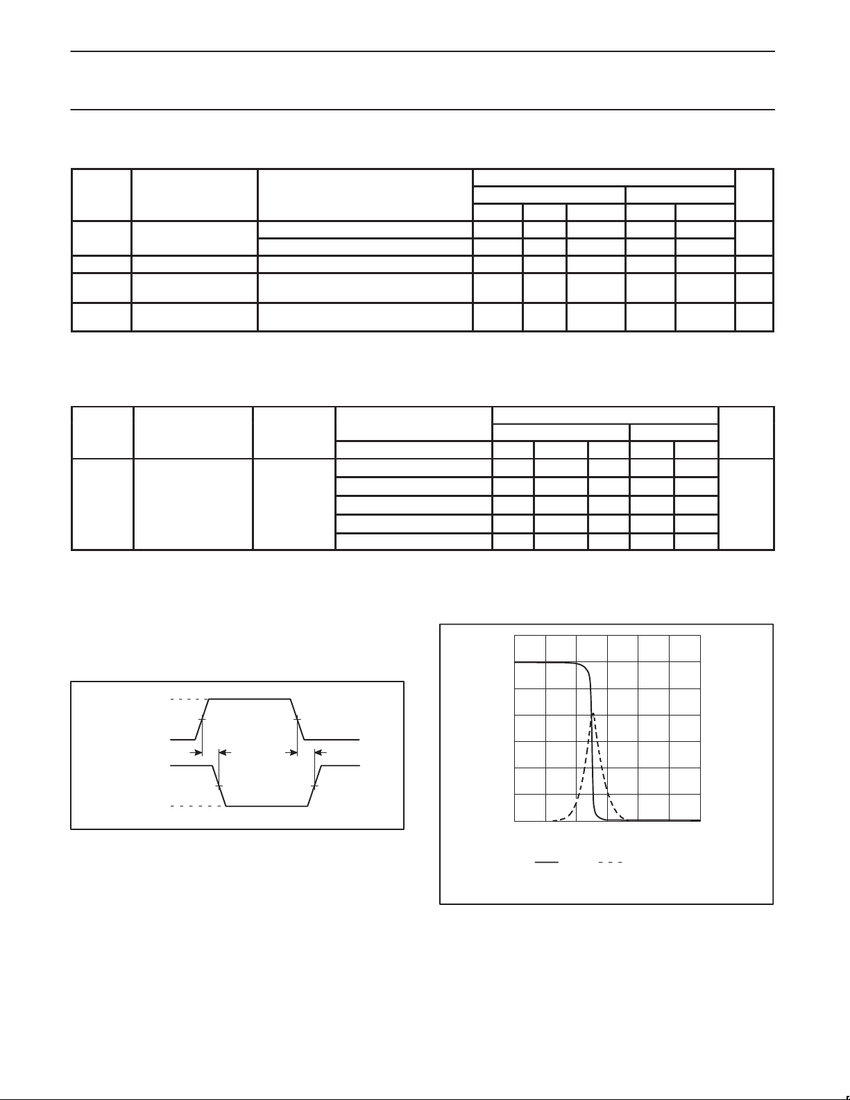
AC WAVEFORMS
VM = 1.5 V at VCC 2.7 V and ≤ 3.6 V
V
= 0.5 × VCC at VCC < 2.7 V and ≥ 4.5 V
M
V
and VOH are the typical output voltage drop that occur with the
OL
output load.
V
I
nA INPUT
GND
V
OH
nY OUTPUT
V
OL
Figure 1. Input (nA) to output (nY) propagation delays
and output transition times.
V
M
t
PHL
V
M
t
PLH
SV00395
TYPICAL TRANSFER CHARACTERISTICS
1.2
V
o
(V)
0.8
0.4
0
0 0.4 0.8
V
O
VCC = 1.2 V; IO = 0 V.
I
Figure 2.
Vi (V)
D
1.2
SV00401
300
200
100
0
I
D
(mA)
1998 Apr 20
5
Page 6

Philips Semiconductors Product specification
Hex inverter
TYPICAL TRANSFER CHARACTERISTICS (
2.0
1.6
V
o
(V)
1.2
0.8
0.4
0
0 0.4 0.8
VCC = 2.0 V; IO = 0 V.
V
O
1.2
Vi (V)
I
D
1.6 2.0
Figure 3.
3.0
V
o
(V)
5
4
3
2
1
0
18
Continued)
I
D
(mA)
SV00402
I
D
(mA)
74LVU04
R
= 560 kW
bias
V
CC
input output
Vi ~
(f = 1 kHz)
Figure 5. Test set-up for measuring forward transconductance
g
= diO/dvi at vO is constant (see also graph Figure 6).
fs
40
30
g
fs
(mA/V)
20
100 mF0.47 mF
i
A
o ~
GND
SV00323
2.0
1.0
12
10
6
0
0
1.0 2.0 3.0
V
O
VCC = 3.0 V; IO = 0 V.
Vi (V)
I
D
0
SV00403
g
fs
0
01234
VCC (V)
Figure 6. Typical forward transconductance
as a function of the supply voltage VCC at T
SV00405
amb
= 25°C.
Figure 4.
1998 Apr 20
6
Page 7

Philips Semiconductors Product specification
Hex inverter
APPLICATION INFORMATION
Some applications for the 74LVU04 are:
•Linear amplifier (see Figure 7)
•In crystal oscillator designs (see Figure 8)
•Astable multivibrator (see Figure 9)
R
2
V
CC
R
1 mF
1
U04
Z
L
GND
Note:
> 10kΩ; AOL = 20 (typical)
Z
L
Au –
3 kΩ < R1, R2 < 1 MΩ
Typical unity gain bandwidth product is 5 MHz.
C
, see Figure10
l
AOL = open loop amplification
Au = voltage amplification
Figure 7. LVU04 used as a linear amplifier.
EXTERNAL COMPONENTS FOR RESONATOR
(f < 1 mHz)
FREQUENCY
(kHz)
10 .. 15.9 2.2 220 56 20
16 .. 24.9 2.2 220 56 10
25 .. 54.9 2.2 100 56 10
55 .. 129.9 2.2 100 47 5
130 .. 199.9 2.2 47 47 5
200 .. 349.9 2.2 47 47 5
350 .. 600 2.2 47 47 5
WHERE:
All values given are typical and must be used as an initial set-up.
A
1
R
1
R
2
OL
(1 AOL)
;V
OMax(PP)
V
≈
at 1/2 V
R1(MW) R2 (KW)
– 1.5 V centered
CC
CC
C1 (pF) C2 (pF)
SV00404
74LVU04
R
1
R
2
U04
out
Note:
C
= 47 pF (typ.)
1
= 22 pF (typ.)
C
2
R
= 1 to 10 MW (typ.)
1
optimum value depends on the frequency and required stability against
R
2
changes in V
2 mA at V
or average minimum ICC (ICC is typically
CC
= 3 V and f = 1 MHz).
CC
Figure 8. Crystal oscillator configuration.
OPTIMUM VALUE FOR R
FREQUENCY
(MHz)
3
6
10
14
> 14 Replace R2 by C3 with a typical value of 35 pF
R
2
(kW)
2.0
Minimum required I
8.0
Minimum influence due to change in V
1.0
Minimum I
4.7
Minimum influence by V
0.5
Minimum I
2.0
Minimum influence by V
0.5
Minimum I
1.0
Minimum influence by V
C
1
2
Optimum
CC
CC
CC
CC
CC
CC
CC
C
2
SV00408
CC
1998 Apr 20
7
Page 8

Philips Semiconductors Product specification
Hex inverter
U04
R
S
Note:
f
RS 2xR
The average I
3.5 + 0.05 x f (MHz) x C (pF) at VCC = 3.0 V.
1
1
T
2.2 RC
(mA) is approximately
CC
R
Figure 9. LVU04 used as an astable multivibrator.
U04
C
SV00406
input
capacitance
(pF)
Note:
1. V
CC
2. V
CC
3. V
CC
80
70
60
50
40
30
20
10
0
= 1.2 V.
= 2.0 V.
= 3.0 V.
1
2
3
0
1
2
input voltage (V)
Figure 10. Typical input capacitance
as function of input voltage.
74LVU04
3
SV00407
Note for Application Information
All values given are typical unless otherwise specified.
1998 Apr 20
8
Page 9

Philips Semiconductors Product specification
Hex inverter
DIP14: plastic dual in-line package; 14 leads (300 mil) SOT27-1
74LVU04
1998 Apr 20
9
Page 10

Philips Semiconductors Product specification
Hex inverter
SO14: plastic small outline package; 14 leads; body width 3.9 mm SOT108-1
74LVU04
1998 Apr 20
10
Page 11

Philips Semiconductors Product specification
Hex inverter
SSOP14: plastic shrink small outline package; 14 leads; body width 5.3 mm SOT337-1
74LVU04
1998 Apr 20
11
Page 12

Philips Semiconductors Product specification
Hex inverter
TSSOP14: plastic thin shrink small outline package; 14 leads; body width 4.4 mm SOT402-1
74LVU04
1998 Apr 20
12
Page 13

Philips Semiconductors Product specification
Hex inverter
74LVU04
NOTES
1998 Apr 20
13
Page 14

Philips Semiconductors Product specification
Hex inverter
74LVU04
DEFINITIONS
Data Sheet Identification Product Status Definition
Objective Specification
Preliminary Specification
Product Specification
Formative or in Design
Preproduction Product
Full Production
This data sheet contains the design target or goal specifications for product development. Specifications
may change in any manner without notice.
This data sheet contains preliminary data, and supplementary data will be published at a later date. Philips
Semiconductors reserves the right to make changes at any time without notice in order to improve design
and supply the best possible product.
This data sheet contains Final Specifications. Philips Semiconductors reserves the right to make changes
at any time without notice, in order to improve design and supply the best possible product.
Philips Semiconductors and Philips Electronics North America Corporation reserve the right to make changes, without notice, in the products,
including circuits, standard cells, and/or software, described or contained herein in order to improve design and/or performance. Philips
Semiconductors assumes no responsibility or liability for the use of any of these products, conveys no license or title under any patent, copyright,
or mask work right to these products, and makes no representations or warranties that these products are free from patent, copyright, or mask
work right infringement, unless otherwise specified. Applications that are described herein for any of these products are for illustrative purposes
only. Philips Semiconductors makes no representation or warranty that such applications will be suitable for the specified use without further testing
or modification.
LIFE SUPPORT APPLICA TIONS
Philips Semiconductors and Philips Electronics North America Corporation Products are not designed for use in life support appliances, devices,
or systems where malfunction of a Philips Semiconductors and Philips Electronics North America Corporation Product can reasonably be expected
to result in a personal injury. Philips Semiconductors and Philips Electronics North America Corporation customers using or selling Philips
Semiconductors and Philips Electronics North America Corporation Products for use in such applications do so at their own risk and agree to fully
indemnify Philips Semiconductors and Philips Electronics North America Corporation for any damages resulting from such improper use or sale.
Philips Semiconductors
811 East Arques Avenue
Copyright Philips Electronics North America Corporation 1998
All rights reserved. Printed in U.S.A.
P.O. Box 3409
Sunnyvale, California 94088–3409
Telephone 800-234-7381
print code Date of release: 05-96
Document order number: 9397-750-04405
1998 Apr 20
14
 Loading...