

Datasheet 74LVTH652WMX, 74LVTH652WM, 74LVTH652MTCX, 74LVTH652MTC Datasheet (Fairchild Semiconductor)
Page 1
© 2000 Fairchild Semiconductor Corporation DS012018 www.fairchildsemi.com
April 2000
Revised April 2000
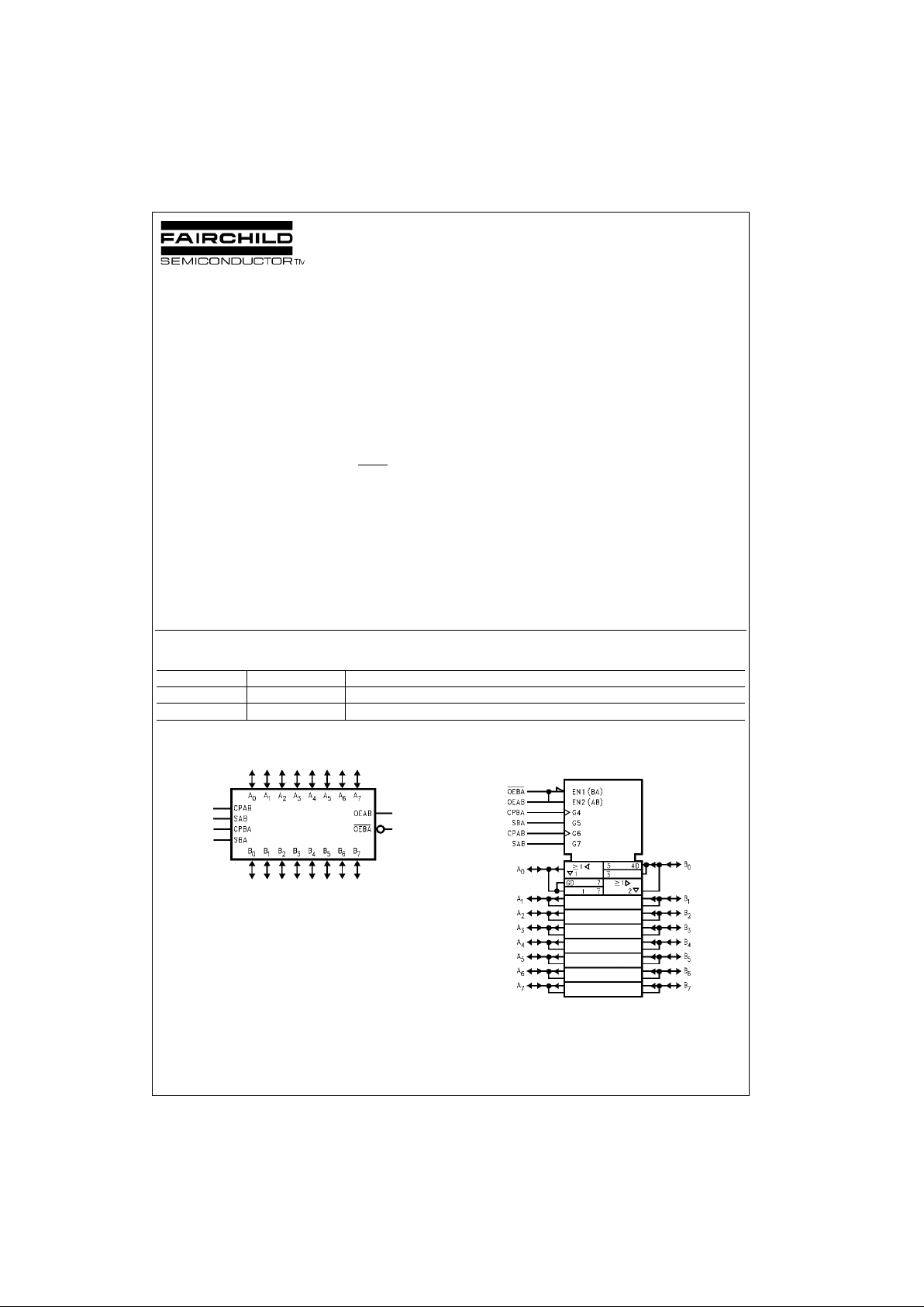
74LVTH652 Low Voltage Octal Trans ceiver/Register with 3-STATE Outputs
74LVTH652
Low Voltage Octal Transceiver/Register
with 3-STATE Outputs
General Description
The LVTH652 consists of bus transceiver circui ts with Dtype flip-flops, and control circuitry arranged for multiplexed
transmission of data d irectly from the in put b us or fr om the
internal registers. Data on the A or B bus will be clocked
into the registers as the appropriate clock pin goes to HIGH
logic level. Output Enable pins (OEAB, OEBA
) are provided to control the tr ansceiver function. (See Functio nal
Description).
The LVTH652 data inputs include bush old, eliminati ng the
need for external pull-up resistors to hold unused inputs.
This octal transceiver/register is d esigned for low-voltage
(3.3V) V
CC
applications, but with the capability to provide a
TTL interface to a 5V enviro nment. The LVTH652 is fabricated with an advanced BiCMOS technology to achieve
high speed opera tion similar to 5V ABT while maintaining
low power dissipation.
Features
■ Input and output interface capability to systems at
5V V
CC
■ Bushold data inputs elimina te the nee d for exte rnal pul lup resistors to hold unused inputs
■ Live insertion/extraction per mitt ed
■ Power Up/Down high impedance provides glitch-free
bus loading
■ Outputs source/sink −32 mA/+64 mA
■ Functionally compatible with the 74 series 652
■ Latch-up performance exceeds 500 mA
Ordering Code:
Devices also availab le in Tape and Reel. Specify by appending su ffix let te r “X” to the ordering code.
Logic Symbols
IEEE/IEC
Order Number Package Number Package Description
74LVTH652WM M24B 24-Lead Small Outline Integrated Circuit (SOIC), JEDEC MS-013, 0.300” Wide
74LVTH652MTC MTC24 24-Lead Thin Shrink Small Outline Package (TSSOP), JEDEC MO-153, 4.4mm Wide
Page 2
www.fairchildsemi.com 2
74LVTH652
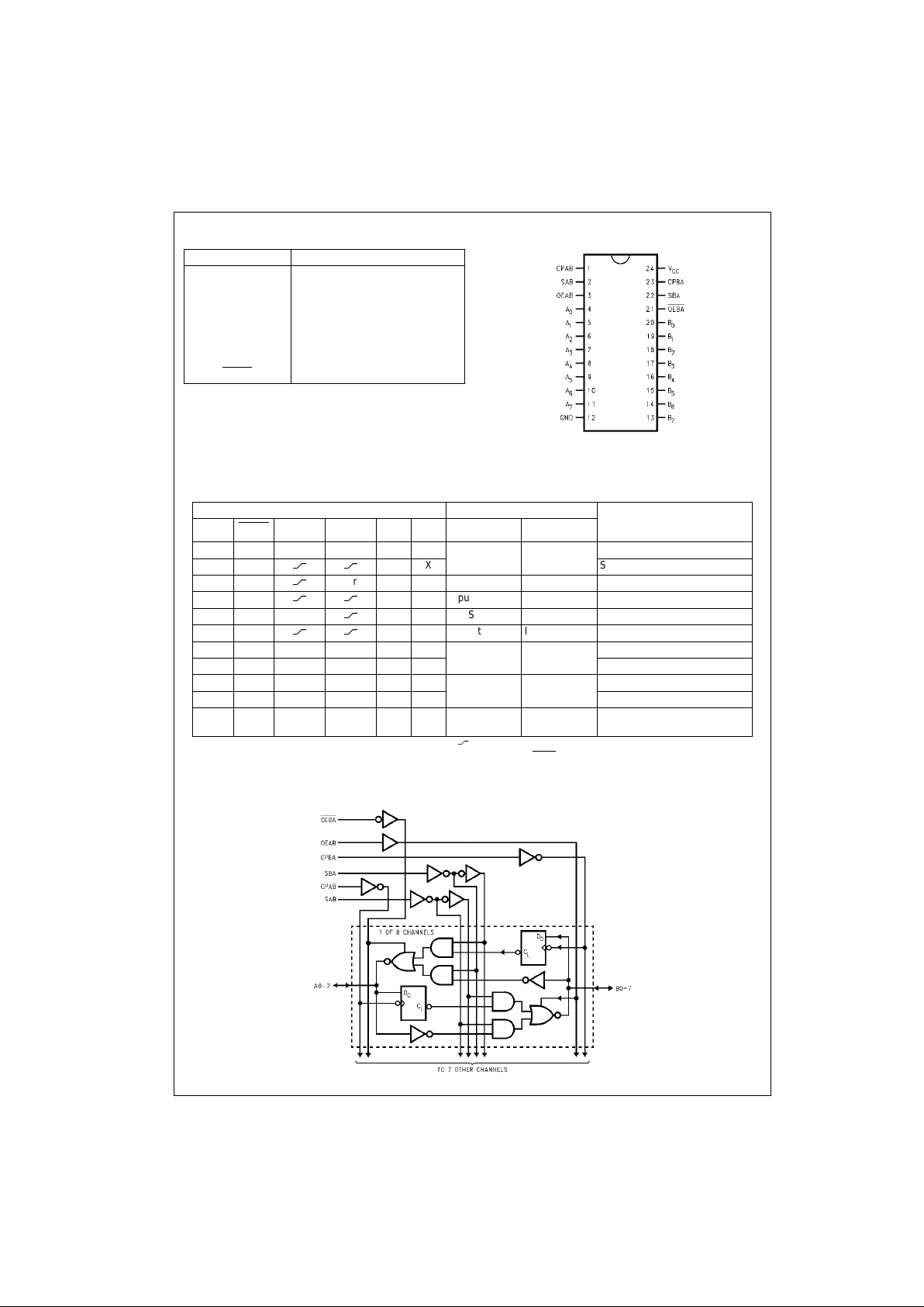
Pin Descriptions Connection Diagram
Truth Table
(Note 1)
H = HIGH Voltage Level L = LOW Voltage Lev el X = Immaterial = LOW to HIGH Clock Transition
Note 1: The data output fu nction s may b e enable d or di sabled b y variou s signa ls at OEA B or O EBA
inputs. Data input function s are a lways e nabled, i.e.,
data at the bus pins w ill be stored on every LOW- to -H I GH t ransition on the clock inp ut s .
Logic Diagram
Please note that this diagram is provided o nly f or t he understanding of lo gic operations and should not be used to estimate propagation delays.
Pin Names Description
A
0–A7
Data Register A Inputs/
3-STATE Outputs
B
0–B7
Data Register B Inputs/
3-STATE Outputs
CPAB, CPBA Clock Pulse Inputs
SAB, SBA Select Inputs
OEAB, OEBA
Output Enable Inputs
Inputs Inputs/Outputs
Operating Mode
OEAB OEBA
CPAB CPBA SAB SBA A0 thru A7B0 thru B
7
L H H or L H or L X X Input Input Isolation
LH
X X Store A and B Data
XH
H or L X X Input Not Specified Store A, Hold B
HH
X X Input Output Store A in Both Registers
LXH or L
X X Not Specified Input Hold A, Store B
LL
X X Output Input Store B in Both Registers
L L X X X L Output Input Real-Time B Data to A Bus
L L X H or L X H Store B Data to A Bus
H H X X L X Input Output Real-Time A Data to B Bus
H H H or L X H X Stored A Data to B Bus
H L H or L H or L H H Output Output
Stored A Data to B Bus and
Stored B Data to A Bus
Page 3
3 www.fairchildsemi.com
74LVTH652
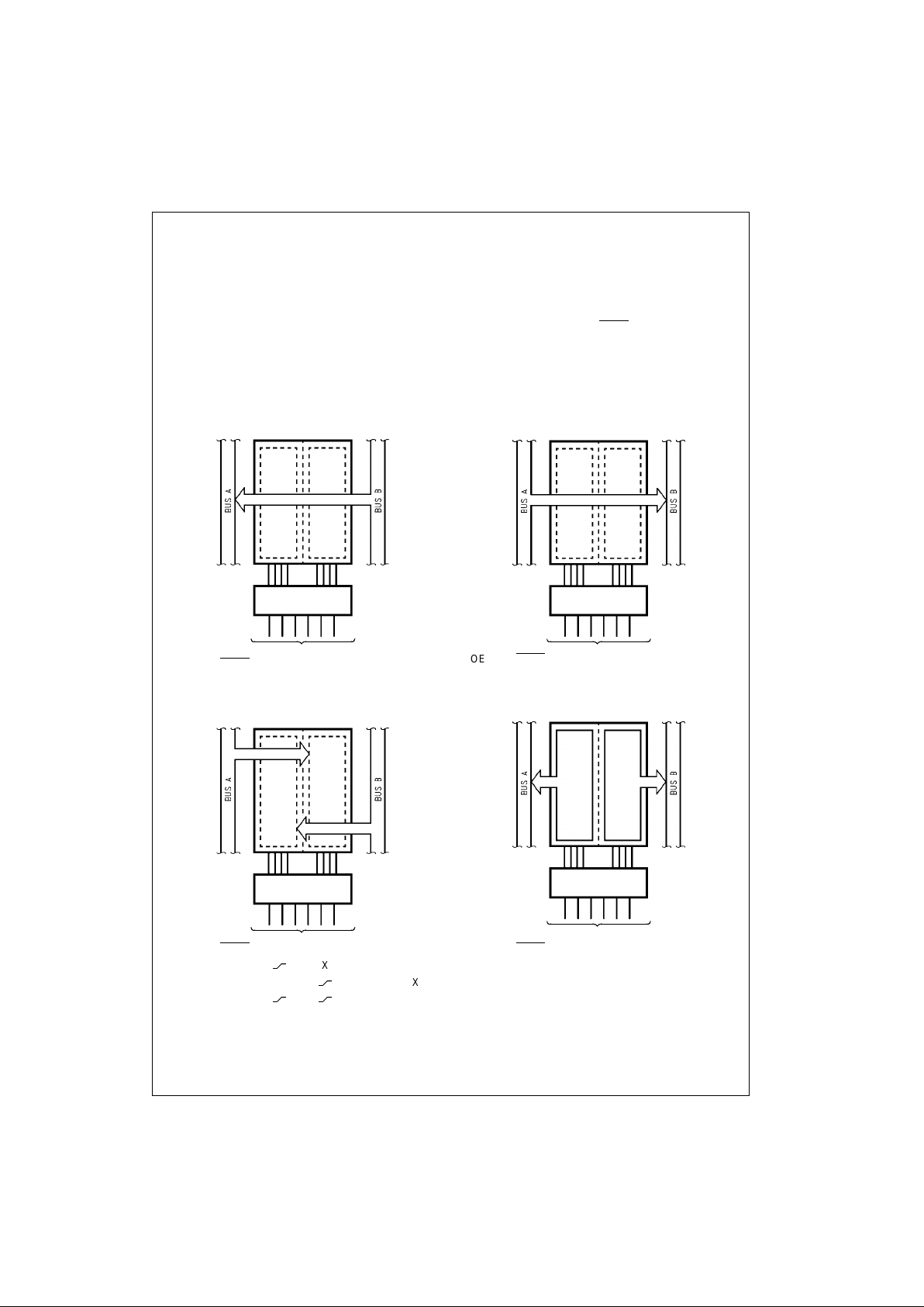
Functional Description
In the transceiver mode , data present a t the HIGH impe dance port may be sto red in either the A or B register or
both.
The select (SAB, SBA) controls can multiplex stored and
real-time.
The examples below demonstrate the four fundamental
bus-management fun cti on s t hat c an be performed wi th t he
LVTH652.
Data on the A or B data bus, or both can be stored in the
internal D-type flip-flop by LOW-to-H IGH transitions at the
appropriate Clock Inp uts (CPAB, CPBA) regardless of the
Select or Output Enable Inputs. When SAB and SBA are in
the real time transfer m od e, it is a lso po ssibl e to sto re d ata
without using the internal D-type flip-flops by simultaneously enabling OEAB and OEBA
. In this configuration
each Output reinforces its Input. Thu s when all other data
sources to the two sets of bus lin es are in a HIGH imp edance state, each set of bus lines will remain at its last state.
Real-Time Transfer
Bus B to Bus A
Storage
Real-Time Transfer
Bus A to Bus B
Transfer Storage
Data to A or B
OEAB OEBA
CPAB CPBA SAB SBA
LLXXXL
OEAB OEBA
CPAB CPBA SAB SBA
XH
XXX
LXX
XX
LH
XX
OEAB OEBA CPAB CPBA SAB SBA
HHXXLX
OEAB OEBA
CPAB CPBA SAB SBA
H L H or L H or L H H
Page 4

www.fairchildsemi.com 4
74LVTH652
Absolute Maximum Ratings(Note 2)
Recommended Operating Conditions
Note 2: Absolute Maximum continuous rat ings are those valu es beyond which da m age to the device m ay occur. Exposure to these conditions or co nditions
beyond those indic ated may adversely affec t device reliability. Functional opera ti on under absolute maximum rated conditio ns is not implied.
Note 3: I
O
Absolute Maximum Rating must be observed.
Symbol Parameter Value Conditions Units
V
CC
Supply Voltage −0.5 to +4.6 V
V
I
DC Input Voltage −0.5 to +7.0 V
V
O
DC Output Voltage −0.5 to +7.0 Output in 3-STATE
V
−0.5 to +7.0 Output in HIGH or LOW State (Note 3)
I
IK
DC Input Diode Current −50 VI < GND mA
I
OK
DC Output Diode Current −50 VO < GND mA
I
O
DC Output Current 64 VO > VCCOutput at HIGH State
mA
128 V
O
> VCCOutput at LOW State
I
CC
DC Supply Current per Supply Pin ±64 mA
I
GND
DC Ground Cu rrent per Ground Pin ±128 mA
T
STG
Storage Temperature −65 to +150 °C
Symbol Parameter Min Max Units
V
CC
Supply Voltage 2.7 3.6 V
V
I
Input Voltage 0 5.5 V
I
OH
HIGH Level Output Current −32 mA
I
OL
LOW Level Output Current 64 mA
T
A
Free-Air Operating Tempera ture −40 85 °C
∆t/∆V Input Edge Rate, V
IN
= 0.8V–2.0V, VCC = 3.0V 0 10 ns/V
Page 5
5 www.fairchildsemi.com
74LVTH652
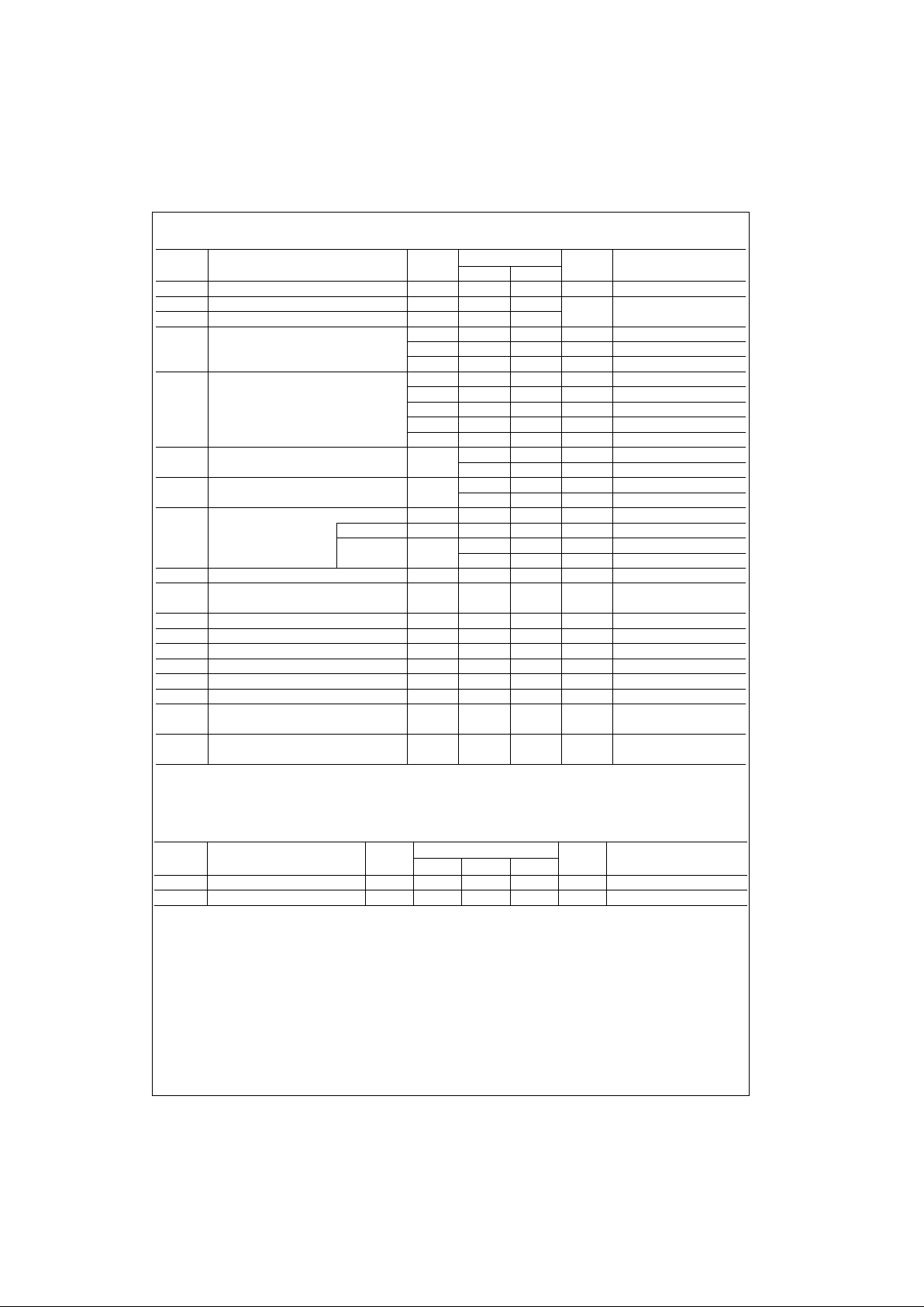
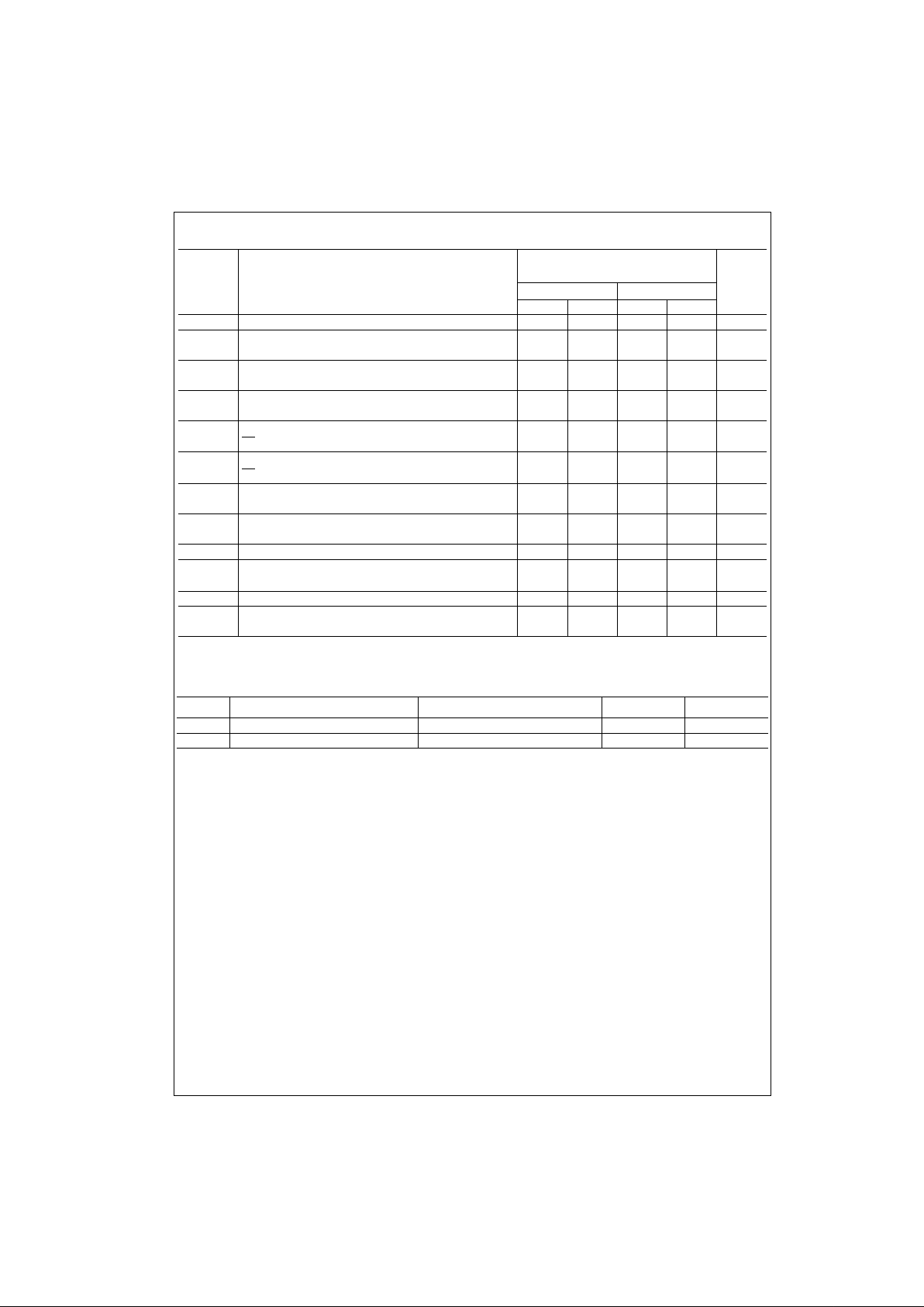
DC Electrical Characteristics
Note 4: An external driver must source at least the specified current to switch from LOW-to-HIGH.
Note 5: An external dri ve r m us t s ink at least the specified cur rent to switch from HIGH -t o-LOW.
Note 6: This is the increas e in supply current for eac h input that is at the specif ied voltage level rather than V
CC
or GND.
Dynamic Switching Characteristics (Note 7)
Note 7: Characterize d in SOIC package. Gu aranteed parameter, but not te sted.
Note 8: Max number of outputs defined as (n). n−1 data inputs are driven 0V to 3V. Output under test held LOW.
Symbol Parameter
V
CC
TA =−40°C to +85°C
Units Conditions
(V) Min Max
V
IK
Input Clamp Diode Voltage 2.7 −1.2 V II = −18 mA
V
IH
Input HIGH Voltage 2.7–3.6 2.0
V
VO ≤ 0.1V or
V
IL
Input LOW Voltage 2.7–3.6 0.8 VO ≥ VCC − 0.1V
V
OH
Output HIGH Voltage 2.7–3.6 VCC − 0.2 V IOH = −100 µA
2.7 2.4 V IOH = −8 mA
3.0 2.0 V IOH = −32 mA
V
OL
Output LOW Voltage 2.7 0.2 V IOL = 100 µA
2.7 0.5 V IOL = 24 mA
3.0 0.4 V IOL = 16 mA
3.0 0.5 V IOL = 32 mA
3.0 0.55 V IOL = 64 mA
I
I(HOLD)
Bushold Input Minimum Drive 3.0 75 µAVI = 0.8V
−75 µAVI = 2.0V
I
I(OD)
Bushold Input Over-Drive 3.0 500 µA (Note 4)
Current to Change State −500 µA (Note 5)
I
I
Input Current 3.6 10 µAVI = 5.5V
Control Pins 3.6 ±1 µAVI = 0V or V
CC
Data Pins 3.6 −5 µAVI = 0V
1 µAVI = V
CC
I
OFF
Power OFF Leakage Current 0 ±100 µA0V ≤ VI or VO ≤ 5.5V
I
PU/PD
Power Up/Down 3-STATE
0–1.5V ±100 µA
VO = 0.5V to 3.0V
Output Current VI = GND or V
CC
I
OZL
3-STATE Output Leakage Current 3.6 −5 µAVO = 0.0V
I
OZH
3-STATE Output Leakage Current 3.6 5 µAVO = 3.6V
I
OZH
+ 3-STATE Output Leakage Current 3.6 10 µAVCC < VO ≤ 5.5V
I
CCH
Power Supply Current 3.6 0.19 mA Outputs HIGH
I
CCL
Power Supply Current 3.6 5 mA A or B Port Outputs LOW
I
CCZ
Power Supply Current 3.6 0.19 mA Outputs Disabled
I
CCZ
+ Power Supply Current 3.6 0.19 mA VCC ≤ VO ≤ 5.5V
Outputs Disabled
∆I
CC
Increase in Power Supply Current
3.6 0.2 mA
One Input at VCC − 0.6V
(Note 6) Other Inputs at VCC or GND
Symbol Parameter
V
CC
TA = 25°C
Units
Conditions
(V) Min Typ Max
CL = 50 pF, RL = 500Ω
V
OLP
Quiet Output Maximum Dynamic V
OL
3.3 0.8 V (Note 8)
V
OLV
Quiet Output Minimum Dynamic V
OL
3.3 −0.8 V (Note 8)
Page 6
www.fairchildsemi.com 6
74LVTH652
AC Electrical Characteristics
Note 9: Skew is defined as t he absolute value of t he difference between t he actual propagat ion delay for any tw o separate outpu ts of the same device. T he
specification applies to any outputs swit c hing in the same direction, eit her HIGH-to-LOW (t
OSHL
) or LOW-to-HIGH (t
OSLH
).
Capacitance (Note 10)
Note 10: Capacitance is measured at frequency f = 1 MHz, per MIL-STD-883B, Method 3012.
Symbol Parameter
TA = −40°C to +85°C
Units
CL = 50 pF, RL = 500Ω
VCC = 3.3V ± 0.3V VCC = 2.7V
Min Max Min Max
f
MAX
Maximum Clock Frequency 150 150 MHz
t
PLH
Propagation Delay Data to Output 1.8 5.6 1.8 6.2
ns
t
PHL
Clock to A or B 1.8 4.8 1.8 5.6
t
PLH
Propagation Delay Data to Output 1.3 4.5 1.3 4.9
ns
t
PHL
Data to A or B 1.3 4.6 1.3 5.2
t
PLH
Propagation Delay Data to Output 1.5 5.5 1.5 6.4
ns
t
PHL
SBA or SAB to A or B 1.5 5.4 1.5 6.1
t
PZH
Output Enable Time 1.1 5.2 1.1 6.5
ns
t
PZL
OE to A
1.1 5.6 1.1 6.6
t
PHZ
Output Disable Time 2.0 5.5 2.0 6.1
ns
t
PLZ
OE to A
2.0 5.5 2.0 5.9
t
PZH
Output Enable Time 1.3 4.9 1.3 5.7
ns
t
PZL
OE to B 1.3 5.3 1.3 5.8
t
PHZ
Output Disable Time 1.5 5.6 1.5 6.7
ns
t
PLZ
OE to B 1.5 5.6 1.5 6.3
t
W
Pulse Duration Clock HIGH or LOW 3.3 3.3 ns
t
S
Setup Time Data HIGH before CP 1.2 1.5
ns
Data LOW before CP
1.6 2.2
t
H
Hold Time Data HIGH or LOW after CP 0.8 0.8 ns
t
OSHL
Output to Output Skew 1.0 1.0
ns
t
OSLH
(Note 9) 1.0 1.0
Symbol Parameter Conditions Typical Units
C
IN
Input Capacitance VCC = 0V, VI = 0V or V
CC
4pF
C
I/O
Input/Output Capacitance VCC = 3.0V, VO = 0V or V
CC
8pF
Page 7
7 www.fairchildsemi.com
74LVTH652
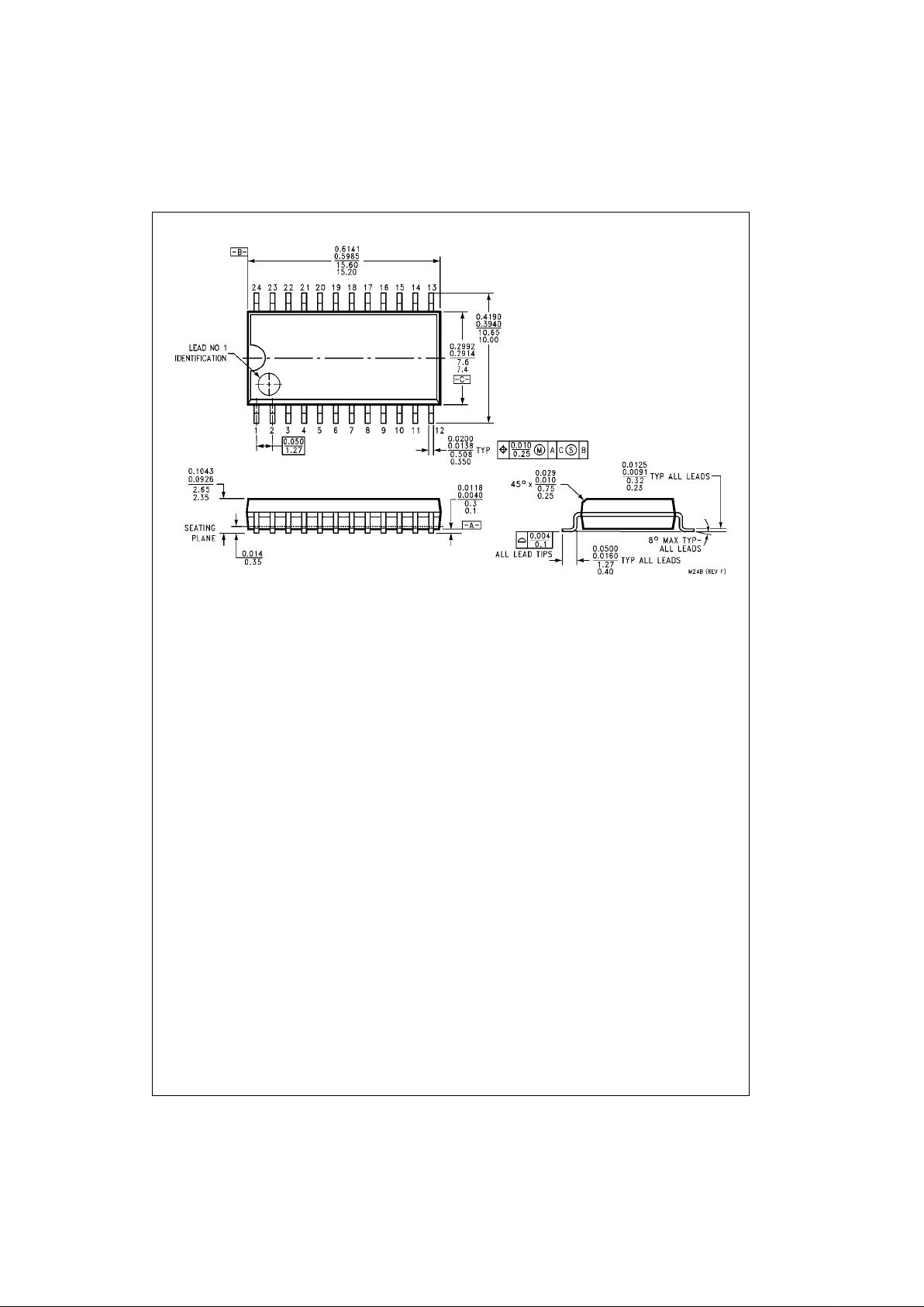
Physical Dimensions inches (millimeters) unless otherwise noted
24-Lead (0.300’ Wide) Molded Small Outline Package, SOIC JEDEC
Package Number M24B
Page 8
www.fairchildsemi.com 8
74LVTH652 Low Voltage Octal Transceiver/Register with 3-STATE Outputs
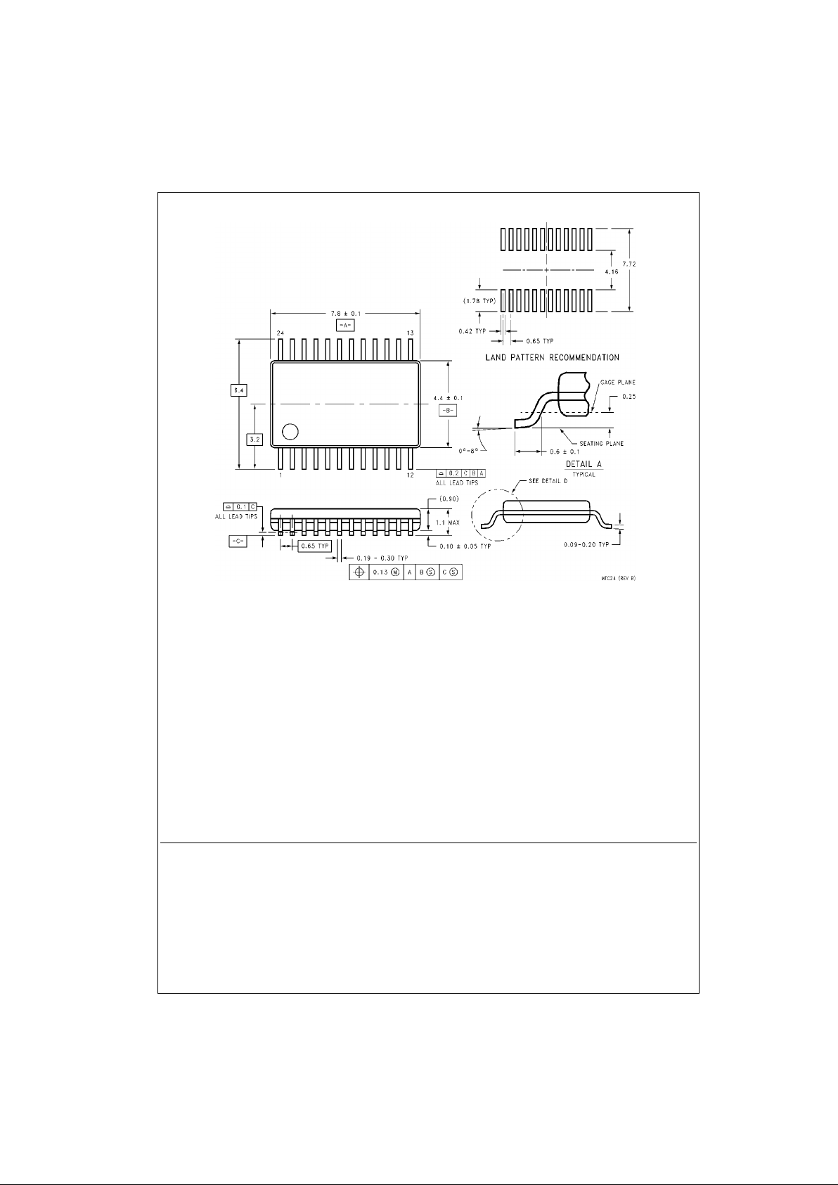
Physical Dimensions inches (millimeters) unless otherwise noted (Continued)
24-Lead Molded Small Outline Package, TSSOP JEDEC
Package Number MTC24
Fairchild does not assume any responsibility for use of any circuitry described, no circuit pate nt licenses are implied and
Fairchild reserves the right at any time without notice to change said circuitry and specifications.
LIFE SUPPORT POLICY
FAIRCHILD’S PRODUCTS ARE NOT AUTHORIZED FOR USE AS CRITICAL COMPONENTS IN LIFE SUPPORT
DEVICES OR SYSTEMS WITHOUT THE EXPRESS WRITTEN APPROVAL OF THE PRESIDENT OF FAIRCHILD
SEMICONDUCTOR CORPORATION. As used herein:
1. Life support devices or systems are devices or syste ms
which, (a) are intended for surgical implant into the
body, or (b) support or sustain life, and (c) whose failure
to perform when properly used in accordance with
instructions for use provided in the labeling, can be reasonably expected to result in a significant inju ry to the
user.
2. A critical component i n any compon ent of a lif e support
device or system whose failu re to perform can be reasonably expected to ca use the fa i lure of the life su pp ort
device or system, or to affect its safety or effectiveness.
www.fairchildsemi.com
 Loading...