

Datasheet 74LVTH574MSAX, 74LVTH574MSA, 74LVTH574WMX, 74LVTH574WM, 74LVTH574SJX Datasheet (Fairchild Semiconductor)
...Page 1
74LVT574 • 74LVTH574
Low Voltage Octal D-Type Flip-Flop
with 3-STAT E Outputs
74LVT574 • 74LVTH574 Low Voltage Octal D-Type Flip-Flop with 3-STATE Outputs
March 1999
Revised March 1999
General Description
The LVT574 and LVTH574 are high-speed, low-power
octal D-type flip-flo p featuring separate D-type in puts for
each flip-flop and 3-STATE outputs for bu s-oriented appl ications. A buffered Clock (CP) and Output Enable (OE
common to all flip-flops.
The LVTH574 data inputs include b ushold, eliminati ng the
need for external pull-up resistors to hold unused inputs.
These octal flip-flop s are designed for low-voltage (3.3V )
applications, but with the capability to provide a TTL
V
CC
interface to a 5V environme nt. The LVT574 and LVTH574
are fabricated with an advanced BiCMOS technology to
achieve high speed operation similar to 5V ABT while
maintaining a low power dissipation.
Features
■ Input and output interface capa bility to systems at 5V
V
CC
■ Bushold data inputs elimina te the nee d for exte rnal pull-
) are
up resistors to hold unused inputs (74LVTH574), also
available without bushold feature (74LVT574).
■ Live insertion/extraction per mitt ed
■ Power Up/Down high impedance provides glitch-free
bus loading
■ Outputs source/sink −32 mA/+64 mA
■ Functionally compatible with the 74 series 574
■ Latch-up performance exce eds 500 mA
Ordering Code:
Order Number Package Number Package Description
74LVT574WM M20B 20-Lead Small Outline Integrated Circuit (SOIC), JEDEC MS-013, .300” Wide
74LVT574SJ M20D 20-Lead Small Outline Package (SOP), EIAJ TYPE II 5.3mm Wide
74LVT574MTC MTC20 20-Lead Thin Shrink Small Outline Package (TSSOP), JEDEC MO-153, 4.4mm Wide
74LVT574MSA MSA20 20-Lead Shrink Small Outline Package (SSOP), EIAJ TYPE II, 5.3mm Wide
74LVTH574WM M20B 20-Lead Small Outline Integrated Circuit (SOIC), JEDEC MS-013, .300” Wide
74LVTH574SJ M20D 20-Lead Small Outline Package (SOP), EIAJ TYPE II 5.3mm Wide
74LVTH574MTC MTC20 20-Lead Thin Shrink Small Outline Package (TSSOP), JEDEC MO-153, 4.4mm Wide
74LVTH574MSA MSA20 20-Lead Shrink Small Outline Package (SSOP), EIAJ TYPE II, 5.3mm Wide
Device also available in Tape and Reel. Specify by appending suffix letter “X” to the ordering code.
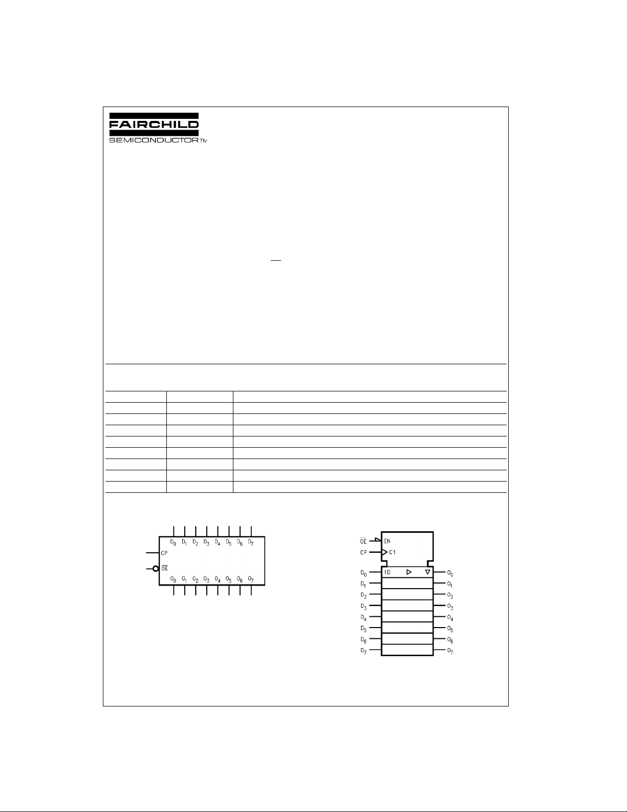
Logic Symbols
IEEE/IEC
© 1999 Fairchild Semiconductor Corporation DS012451.prf www.fairchildsemi.com
Page 2
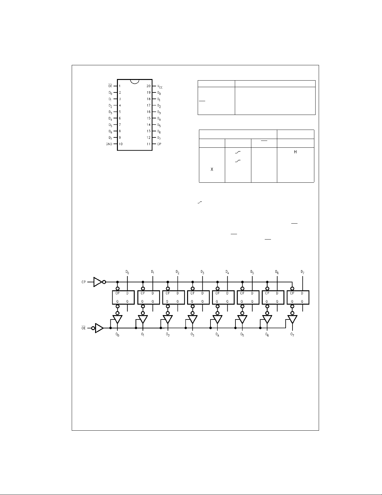
Connection Diagram Pin Descriptions
Pin Names Description
D
0–D7
Data Inputs
CP Clock Pulse Input
OE
O
0–O7
3-STATE Output Enable Input
3-STATE Outputs
Truth Table
74LVT574 • 74LVTH574
Functional Description
The LVT574 and LVTH574 consist of eigh t edge-trigg ered
flip-flops with individual D-type inputs and 3-STATE true
outputs. The buffered clock and buffered Output Enable
are common to all flip-flops. The eight flip-flops will store
the state of their individual D-type inputs that meet the
setup and hold time requirements on the LOW-to-HIGH
Logic Diagram
Inputs Outputs
D
n
H
L
XLL O
CP OE O
LH
LL
n
o
XXH Z
H = HIGH Voltage Level
L = LOW Voltage Level
X = Immaterial
Z = High Impedance
= LOW-to-HIGH Transition
= Previous Oo before HIGH to LOW of CP
O
o
Clock (CP) transition . With the Output Enable (OE
) LOW,
the contents of the eight flip -flops are av ailable at the outputs. When the OE
impedance state. Operation of the OE
is HIGH, the outputs go to the high
input does not affect
the state of the flip-flops.
Please note that this diagram is provided only for the understan ding of logic operations and should not be used to estimate propaga tio n delays.
www.fairchildsemi.com 2
Page 3
Absolute Maximum Ratings(Note 1)
Symbol Parameter Value Conditions Units
V
CC
V
I
V
O
Supply Voltage −0.5 to +4.6 V
DC Input Voltage −0.5 to +7.0 V
DC Output Voltage −0.5 to +7.0 Output in 3-STATE
−0.5 to +7.0 Output in High or Low State (Note 2)
I
IK
I
OK
I
O
I
CC
I
GND
T
STG
DC Input Diode Current −50 VI < GND mA
DC Output Diode Current −50 VO < GND mA
DC Output Current 64 VO > VCCOutput at High State
128 V
> VCCOutput at Low State
O
mA
DC Supply Current per Supply Pin ±64 mA
DC Ground Current per Ground Pin ±128 mA
Storage Temperature −65 to +150 °C
Recommended Operating Conditions
Symbol Parameter Min Max Units
V
CC
V
I
I
OH
I
OL
T
A
∆t/∆V Input Edge Rate, V
Note 1: Absolute Maximum continuous ratings are those values beyond which damage to the device may occur. Exposure to these conditions or conditions
beyond those indica te d m ay adversely affect de v ic e reliability. Functional operation under absolute maxim um rated conditions is no t implied.
Note 2: I
Supply Voltage 2.7 3.6 V
Input Voltage 0 5.5 V
High-Level Output Current −32 mA
Low-Level Output Current 64 mA
Free-Air Operating Temperature −40 85 °C
= 0.8V–2.0V, VCC = 3.0V 0 10 ns/V
IN
Absolute Maximum Rating must be observed.
O
74LVT574 • 74LVTH574
V
DC Electrical Characteristics
V
Symbol Parameter
V
IK
V
IH
V
IL
V
OH
V
OL
I
I(HOLD)
(Note 4) −75 VI = 2.0V
I
I(OD)
(Note 4) −500 (Note 6)
I
I
I
OFF
I
PU/PD
I
OZL
I
OZH
Input Clamp Diode Voltage 2.7 −1.2 V II = −18 mA
Input HIGH Voltage 2.7–3.6 2.0 V VO ≤ 0.1V or
Input LOW Voltage 2.7–3.6 0.8 V
Output HIGH Voltage 2.7–3.6 VCC − 0.2
Output LOW Voltage 2.7 0.2
Bushold Input Minimum Drive 3.0 75
Bushold Input Over-Drive
Current to Change State
Input Current 3.6 10
Power Off Leakage Current 0 ±100 µA0V ≤ VI or VO ≤ 5.5V
Power up/down 3-STATE 0–1.5V ±100 µAVO = 0.5V to 3.0V
Output Current VI = GND or V
3-STATE Output Leakage Current 3.6 −5 µAVO = 0.5V
3-STATE Output Leakage Current 3.6 5 µAVO = 3.0V
Control Pins 3.6 ±1V
Data Pins 3.6 −5V
CC
(V)
2.7 2.4 IOH = −8 mA
3.0 2.0 IOH = −32 mA
2.7 0.5 IOL = 24 mA
3.0 0.4 IOL = 16 mA
3.0 0.5 IOL = 32 mA
3.0 0.55 IOL = 64 mA
3.0 500
T A = −40°C to +85°C
Min Typ Max
(Note 3)
Units Conditions
VO ≥ VCC − 0.1V
IOH = −100 µA
V
IOL = 100 µA
V
VI = 0.8V
µA
(Note 5)
µA
VI = 5.5V
= 0V or V
I
µA
= 0V
1V
I
I
= V
CC
CC
CC
3 www.fairchildsemi.com
Page 4

DC Electrical Characteristics (Continued)
V
Symbol Parameter
I
+ 3-STATE Output Leakage Current 3.6 10 µAVCC < VO ≤ 5.5V
OZH
I
I
I
I
CCH
CCL
CCZ
CCZ
Power Supply Current 3.6 0.19 mA Outputs High
Power Supply Current 3.6 5 mA Outputs Low
Power Supply Current 3.6 0.19 mA Outputs Disabled
+ Power Supply Current 3.6 0.19 mA VCC ≤ VO ≤ 5.5V,
CC
(V)
74LVT574 • 74LVTH574
∆I
CC
Increase in Power Supply Current 3.6 0.2 mA One Input at VCC − 0.6V
T A = −40°C to +85°C
Min Typ Max
(Note 3)
Units Conditions
Outputs Disabled
(Note 7) Other Inputs at VCC or GND
Note 3: All typical va lues are at VCC = 3.3V, TA = 25°C.
Note 4: Applies to bu s hold versions only (7 4LVTH574).
Note 5: An externa l driv er must source at lea s t the specified current to s w it c h f rom LOW to HIGH.
Note 6: An externa l driv er must sink at least the specified current to s w it c h f rom H I GH to LOW.
Note 7: This is the increase in supply curr ent f or each input that is at the specified voltage level rather than V
or GND.
CC
Dynamic Switching Characteristics (Note 8)
V
Symbol Parameter
V
OLP
V
OLV
Note 8: Characteriz ed in SOIC packag e. Guaranteed paramet er, but not tes t ed.
Note 9: Max number of outputs defined as (n). n−1 data inputs ar e driven 0V to 3V. Output under test hel d LOW.
Quiet Output Maximum Dynamic V
Quiet Output Minimum Dynamic V
OL
OL
CC
(V)
3.3 0.8 V (Note 9)
3.3 −0.8 V (Note 9)
TA = 25°C
Min Typ Max
Units
AC Electrical Characteristics
TA = −40°C to +85°C
CL = 50 pF, RL = 500Ω
Symbol Parameter
f
MAX
t
PHL
t
PLH
t
PZL
t
PZH
t
PLZ
t
PHZ
t
S
t
H
t
W
t
OSHL
t
OSLH
Note 10: All typical v alues are at VCC = 3.3V, TA = 25°C.
Note 11: Skew is defined as the ab s olute value of the difference between the actual propagation delay for any two separate outputs of the same device. The
specification applies to any outputs sw it c hing in the same directi on, eit her HIGH to LOW (t
Maximum Clock Frequency 150 150 MHz
Propagation Delay 1.8 4.6 1.8 5.3
CP to O
n
Output Enable Time 1.5 5.2 1.5 6.1
Output Disable Time 2.0 4.4 2.0 4.4
Setup Time 2.0 2.4 ns
Hold Time 0.3 0.0 ns
Pulse Width 3.3 3.3 ns
Output to Output Skew (Note 11) 1.0 1.0
VCC = 3.3V ±0.3V VCC = 2.7V
Min
Typ
(Note 10)
Max Min Max
1.8 4.5 1.8 5.3
1.5 4.8 1.5 5.9
2.0 4.8 2.0 5.1
1.0 1.0
) or LOW to HIGH (t
OSHL
OSLH
).
Conditions
CL = 50 pF,
RL = 500Ω
Units
ns
ns
ns
ns
Capacitance (Note 12)
Symbol Parameter Conditions Typical Units
C
IN
C
OUT
Note 12: Capacitance is measured at f requency f = 1 MHz, per MIL-STD-883, Method 3012.
www.fairchildsemi.com 4
Input Capacitance VCC = Open, VI = 0V or V
Output Capacitance VCC = 3.0V, VO = 0V or V
CC
CC
4pF
6pF
Page 5

Physical Dimensions inches (millimeters) unless otherwise noted
74LVT574 • 74LVTH574
20-Lead Small Outline Integrated Circuit (SOIC), JEDEC MS-013, .300” Wide
20-Lead Small Outline Package (SOP), EIAJ TYPE II 5.3mm Wide
Package Number M20B
Package Number M20D
5 www.fairchildsemi.com
Page 6

Physical Dimensions inches (millimeters) unless otherwise noted (Continued)
74LVT574 • 74LVTH574
20-Lead Thin Shrink Small Outline Package (TSSOP), JEDEC MO-153, 4.4mm Wide
www.fairchildsemi.com 6
Package Number MTC20
Page 7

Physical Dimensions inches (millimeters) unless otherwise noted (Continued)
74LVT574 • 74LVTH574 Low Voltage Octal D-Type Flip-Flop with 3-STATE Outputs
20-Lead Shrink Small Outline Package (SSOP), EIAJ TYPE II, 5.3mm Wide
LIFE SUPPORT POLICY
FAIRCHILD’S PRODUCTS ARE NOT AUTHORIZED FOR USE AS CRITICAL COMPONENTS IN LIFE SUPPORT
DEVICES OR SYSTEMS WITHOUT THE EXPRESS WRITTEN APPROVAL OF THE PRESIDENT OF FAIRCHILD
SEMICONDUCTOR CORPORATION. As used herein:
1. Life support devices or systems are devices or systems
which, (a) are intended for surgical implant into the
body, or (b) support or sustain life, and (c) whose failure
to perform when properly used in accordance with
instructions for use provide d in the labe l ing, can be re asonably expected to result in a significant injury to the
user.
Package Number MSA20
2. A critical componen t in any com ponen t of a life s upport
device or system whose failu re to perform can b e reasonably expected to cause the failure of the li fe s upp or t
device or system, or to affect its safety or effectiveness.
www.fairchildsemi.com
Fairchild does not assume any responsibility for use of any circuitry described, no circuit patent licenses are implied and Fairchild reserves the right at any time without notice to change said circuitry and specifications.
 Loading...