

Datasheet 74LVTH543WMX, 74LVTH543WM, 74LVTH543MTCX, 74LVTH543MTC Datasheet (Fairchild Semiconductor)
Page 1
© 2000 Fairchild Semiconductor Corporation DS012448 www.fairchildsemi.com
April 2000
Revised April 2000
74LVTH543 Low Voltage Octal Registered Transceiver with 3-STATE Outputs
74LVTH543
Low Voltage Octal Registered Transceiver
with 3-STATE Outputs
General Description
The LVTH543 octal transceiver contains two sets of D-type
latches for temporary storage of data flowing in either
direction. Separate Latch Enable and Output Enable inputs
are provided for each reg ister to permit indep endent control of inputting and outputt ing in either direction of data
flow.
The LVTH543 data inputs include bush old, eliminati ng the
need for external pull-up resistors to hold unused inputs.
This octal registere d transceiver is designed for low-voltage (3.3V) V
CC
applications, but with the capability to pro-
vide a TTL interface to a 5V environment. The LVTH543 is
fabricated with an advanced BiCMOS technology to
achieve high speed operation similar to 5V ABT while
maintaining a low power dissipation.
Features
■ Input and output interface capability to systems at
5V V
CC
■ Bushold data inputs elimina te the nee d for exte rnal pul lup resistors to hold unused inputs
■ Live insertion/extraction per mitt ed
■ Power Up/Down high impedance provides glitch-free
bus loading
■ Outputs source/sink −32 mA/+64 mA
■ Functionally compatible with the 74 series 543
■ Latch-up performance exceeds 500 mA
Ordering Code:
Device also available in Tape and Reel. Specify by appending s uffix let te r “X” to the ordering code.
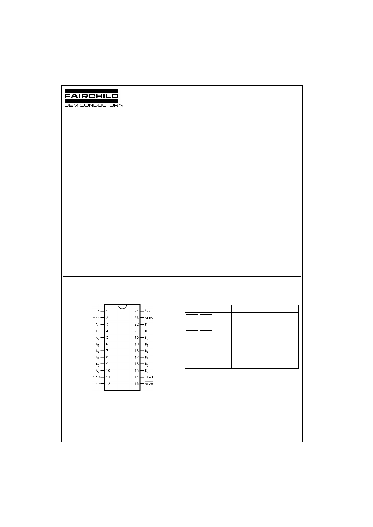
Connection Diagram Pin Descriptions
Order Number Package Number Package Description
74LVTH543WM M24B 24-Lead Small Outline Integrated Circuit (SOIC), JEDEC MS-013, 0.300” Wide
74LVTH543MTC MTC24 24-Lead Thin Shrink Small Outline Package (TSSOP), JEDEC MO-153, 4.4mm Wide
Pin Names Description
OEAB
, OEBA Output Enable Inputs
LEAB
, LEBA Latch Enable Inputs
CEAB
, CEBA Chip Enable Inputs
A
0–A7
Side A Inputs or
3-STATE Outputs
B
0–B7
Side B Inputs or
3-STATE Outputs
Page 2
www.fairchildsemi.com 2
74LVTH543
Logic Symbols
IEEE/IEC
Functional Description
The LVTH543 contains two sets of D-type latches, with
separate input and output cont rols for each. For data flo w
from A to B, for example, the A to B Enable (CEAB
) input
must be LOW in order to enter data from the A Port or take
data from the B Port as indicated in the Data I/O Control
Table. With CEAB
LOW, a low signal on (LEAB) input
makes the A to B latches transparent; a subseq uent LOWto-HIGH transition of the LEAB
line puts the A latches in
the storage mode and their outputs no longer change with
the A inputs. With CEAB
and OEAB both LOW, the B output buffers are active an d reflect the data prese nt on the
output of the A latches. C ontrol of data flow from B to A is
similar, but using the CEBA
, LEBA and OEBA.
Data I/O Control Table
H = HIGH Voltage Level
L = LOW Voltage Level
X = Immaterial
Note: A-to-B data flow s hown; B-to-A flow control is t he same, except
using CEBA
, LEBA, and OEBA.
Logic Diagram
Please not that this diagram is provided on ly fo r th e understanding of logic operations and should not be used to estimate propagation delays.
Inputs
Latch Status
Output
CEAB
LEAB OEAB Buffers
H X X Latched High Z
X H X Latched —
L L X Transparent —
XXH — High Z
L X L — Driving
Page 3
3 www.fairchildsemi.com
74LVTH543
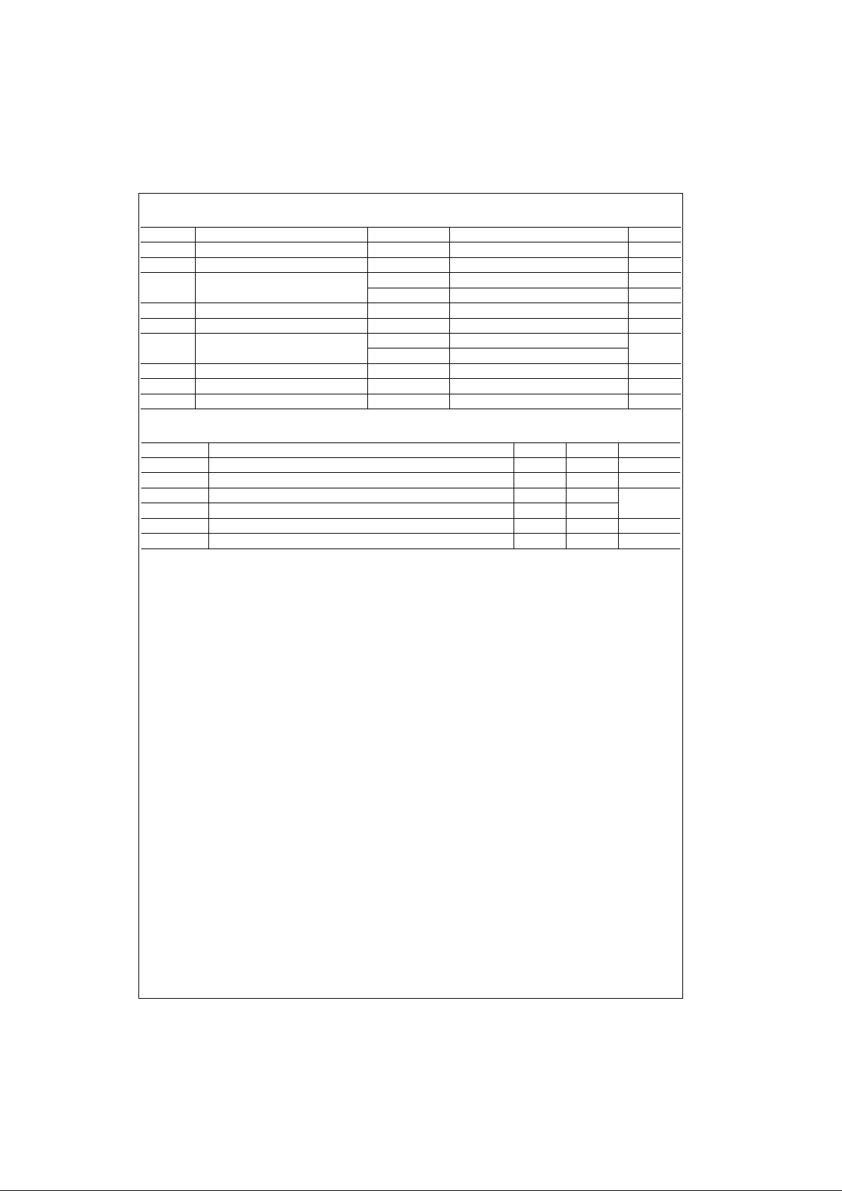
Absolute Maximum Ratings(Note 1)
Recommended Operating Conditions
Note 1: Absolute Maximum continuous ratings are those values beyond which damage to the device may occur. Exposure to these conditions or conditions
beyond those indica te d m ay adversely affect dev ic e reliability. Functional operation under absolute maxim um rated conditions is not imp lied.
Note 2: I
O
Absolute Maximum Rating must be observed.
Symbol Parameter Value Conditions Units
V
CC
Supply Voltage −0.5 to +4.6 V
V
I
DC Input Voltage −0.5 to +7.0 V
V
O
DC Output Voltage −0.5 to +7.0 Output in 3-STATE V
−0.5 to +7.0 Output in HIGH or LOW State (Note 2) V
I
IK
DC Input Diode Current −50 VI < GND mA
I
OK
DC Output Diode Current −50 VO < GND mA
I
O
DC Output Current 64 VO > VCCOutput at HIGH State
mA
128 V
O
> VCCOutput at LOW State
I
CC
DC Supply Current per Supply Pin ±64 mA
I
GND
DC Ground Current per Ground Pin ±128 mA
T
STG
Storage Temperature −65 to +150 °C
Symbol Parameter Min Max Units
V
CC
Supply Voltage 2.7 3.6 V
V
I
Input Voltage 0 5.5 V
I
OH
HIGH Level Output Current −32
mA
I
OL
LOW Level Output Current 64
T
A
Free-Air Operating Tempera ture −40 85 °C
∆t/∆V Input Edge R ate, V
IN
= 0.8V–2.0V, VCC = 3.0V 0 10 ns/V
Page 4

www.fairchildsemi.com 4
74LVTH543
DC Electrical Characteristics
Note 3: An externa l driv er must source at leas t the specified current to s w it c h f rom LOW-to-HIGH.
Note 4: An externa l driv er must sink at least the sp ec if ied current to switch from H I GH-to-LOW.
Note 5: This is the increase in supply current f or each input that is at the spe c if ied voltage level rather t han V
CC
or GND.
Dynamic Switching Characteristics (Note 6)
Note 6: Characteriz ed in SOIC package. Guaranteed parameter, but not tes t ed.
Note 7: Max number of outputs defined a s (n ). n−1 data inputs are driven 0V to 3V. Output under test held LOW.
Symbol Parameter
V
CC
TA =−40°C to +85°C
Units Conditions
(V) Min Max
V
IK
Input Clamp Diode Voltage 2.7 −1.2 V II = −18 mA
V
IH
Input HIGH Voltage 2.7–3.6 2.0
V
VO ≤ 0.1V or
V
IL
Input LOW Voltage 2.7–3.6 0.8 VO ≥ VCC − 0.1V
V
OH
Output HIGH Voltage 2.7–3.6 VCC − 0.2 V IOH = −100 µA
2.7 2.4 V IOH = −8 mA
3.0 2.0 V IOH = −32 mA
V
OL
Output LOW Voltage 2.7 0.2 V IOL = 100 µA
2.7 0.5 V IOL = 24 mA
3.0 0.4 V IOL = 16 mA
3.0 0.5 V IOL = 32 mA
3.0 0.55 V IOL = 64 mA
I
I(HOLD)
Bushold Input Minimum Drive 3.0 75 µAVI = 0.8V
−75 µAVI = 2.0V
I
I(OD)
Bushold Input Over-Drive 3.0 500 µA(Note 3)
Current to Change State −500 µA(Note 4)
I
I
Input Current 3.6 10 µAVI = 5.5V
Control Pins 3.6 ±1 µAVI = 0V or V
CC
Data Pins 3.6 −5 µAVI = 0V
1 µAVI = V
CC
I
OFF
Power Off Leakage Current 0 ±100 µA0V ≤ VI or VO ≤ 5.5V
I
PU/PD
Power Up/Down 3-STATE 0–1.5V ±100 µAVO = 0.5V to 3.0V
Output Current VI = GND or V
CC
I
OZL
3-STATE Output Leakage Current 3.6 −5 µAVO = 0.0V
I
OZH
3-STATE Output Leakage Current 3.6 5 µAVO = 3.6V
I
OZH
+ 3-STATE Output Leakage Current 3.6 10 µAVCC < VO ≤ 5.5V
I
CCH
Power Supply Current 3.6 0.19 mA Outputs HIGH
I
CCL
Power Supply Current 3.6 5 mA A or B Port Outputs LOW
I
CCZ
Power Supply Current 3.6 0.19 mA Outputs Disabled
I
CCZ
+ Power Supply Current 3.6 0.19 mA VCC ≤ VO ≤ 5.5V
Outputs Disabled
∆I
CC
Increase in Power Supply Current 3.6 0.2 mA One Input at VCC − 0.6V
(Note 5) Other Inputs at VCC or GND
Symbol Parameter
V
CC
TA = 25°C
Units
Conditions
(V) Min Typ Max
CL = 50 pF, RL = 500Ω
V
OLP
Quiet Output Maximum Dynamic V
OL
3.3 0.8 V (Note 7)
V
OLV
Quiet Output Minimum Dynamic V
OL
3.3 −0.8 V (Note 7)
Page 5

5 www.fairchildsemi.com
74LVTH543
AC Electrical Characteristics
Note 8: Skew is def ined as the absol ut e v alue of the difference between the actu al propagation del ay f or any two separate outputs of the same device. The
specification applies t o any outputs switching in the same direction, ei th er HIGH-to-LOW (t
OSHL
) or LOW-to-HIGH (t
OSLH
).
Capacitance (Note 9)
Note 9: Capacitance is m eas ured at frequency f = 1 MHz, per MIL-STD-883B, Method 3012.
Symbol Parameter
TA = −40°C to +85°C
Units
CL = 50 pF, RL = 500Ω
VCC = 3.3V ± 0.3V VCC = 2.7V
MinMaxMinMax
t
PLH
Propagation Delay 1.3 4.4 1.3 4.8
ns
t
PHL
Data to Outputs 1.3 4.6 1.3 5.2
t
PLH
Propagation Delay 1.3 5.4 1.3 6.4
ns
t
PHL
LE to A or B 1.3 5.8 1.3 6.6
t
PZH
Output Enable Time 1.1 5.5 1.1 6.3
ns
t
PZL
OE to A or B 1.1 6.1 1.1 7.2
t
PHZ
Output Disable Time 2.0 5.7 2.0 5.9
ns
t
PLZ
OE to A or B 2.0 5.3 2.0 5.9
t
PZH
Output Enable Time 1.3 5.9 1.3 6.8
ns
t
PZL
CE to A or B 1.3 6.2 1.3 7.4
t
PHZ
Output Disable Time 2.1 5.8 2.1 6.1
ns
t
PLZ
CE to A or B 1.6 5.4 1.6 5.9
t
W
Pulse Duration
LE LOW
3.3 3.3 ns
t
S
Setup Time
A or B before LE, Data HIGH
0.4 0.4
ns
A or B before LE, Data LOW
1.0 1.5
A or B before CE, Data HIGH
0.2 0.2
A or B before CE, Data LOW
0.7 1.2
t
H
Hold Time
A or B before LE, Data HIGH
1.5 0.6
ns
A or B before LE, Data LOW
1.3 1.5
A or B before CE, Data HIGH
1.6 0.5
A or B before CE, Data LOW
1.4 1.6
t
OSHL
Output to Output Skew (Note 8) 1.0 1.0
ns
t
OSLH
1.0 1.0
Symbol Parameter Conditions Typical Units
C
IN
Input Capacitance VCC = 0V, VI = 0V or V
CC
4pF
C
I/O
Input/Output Capacitance VCC = 3.0V, VO = 0V or V
CC
8pF
Page 6

www.fairchildsemi.com 6
74LVTH543
Physical Dimensions inches (millimeters) unless otherwise noted
24-Lead Small Outline Integrated Circuit (SOIC), JEDEC MS-013, 0.300” Wide
Package Number M24B
Page 7

7 www.fairchildsemi.com
74LVTH543 Low Voltage Octal Registered Transceiver with 3-STATE Outputs
Physical Dimensions inches (millimeters) unless otherwise noted (Continued)
24-Lead Thin Shrink Small Outline Package (TSSOP), JEDEC MO-153, 4.4mm Wide
Package Number MTC24
Fairchild does not assume any responsibility for use of any circu itry described, no circuit patent license s are implied and
Fairchild reserves the right at any time without notice to change said circuitry and specifications.
LIFE SUPPORT POLICY
FAIRCHILD’S PRODUCTS ARE NOT AUTHORIZED FOR USE AS CRITICAL COMPONENTS IN LIFE SUPPORT
DEVICES OR SYSTEMS WITHOUT THE EXPRESS WRITTEN APPROVAL OF THE PRESIDENT OF FAIRCHILD
SEMICONDUCTOR CORPORATION. As used herein:
1. Life support devices or systems are dev ic es or syste ms
which, (a) are intended for surgical implant into the
body, or (b) support or sustain life, and (c) whose failure
to perform when properly used in accordance with
instructions for use provided i n the labe li ng, can be re asonably expected to result in a significant injury to the
user.
2. A critical componen t in any com ponent o f a l ife supp ort
device or system whose failu re to perform can b e reasonably expected to c ause th e fa i lure of the li fe s upp or t
device or system, or to affect its safety or effectiveness.
www.fairchildsemi.com
 Loading...