

Page 1
74LVT32244 • 74LVTH32244
Low Voltage 32-Bit Buffer/Line Driver
with 3-STATE Outputs (Preliminary)
Preliminary
74LVT32244 • 74LVTH32244 Low Voltage 32-Bit Buffer/Line Driver with 3-STATE Outputs (Preliminary)
January 2001
Revised August 2001
General Description
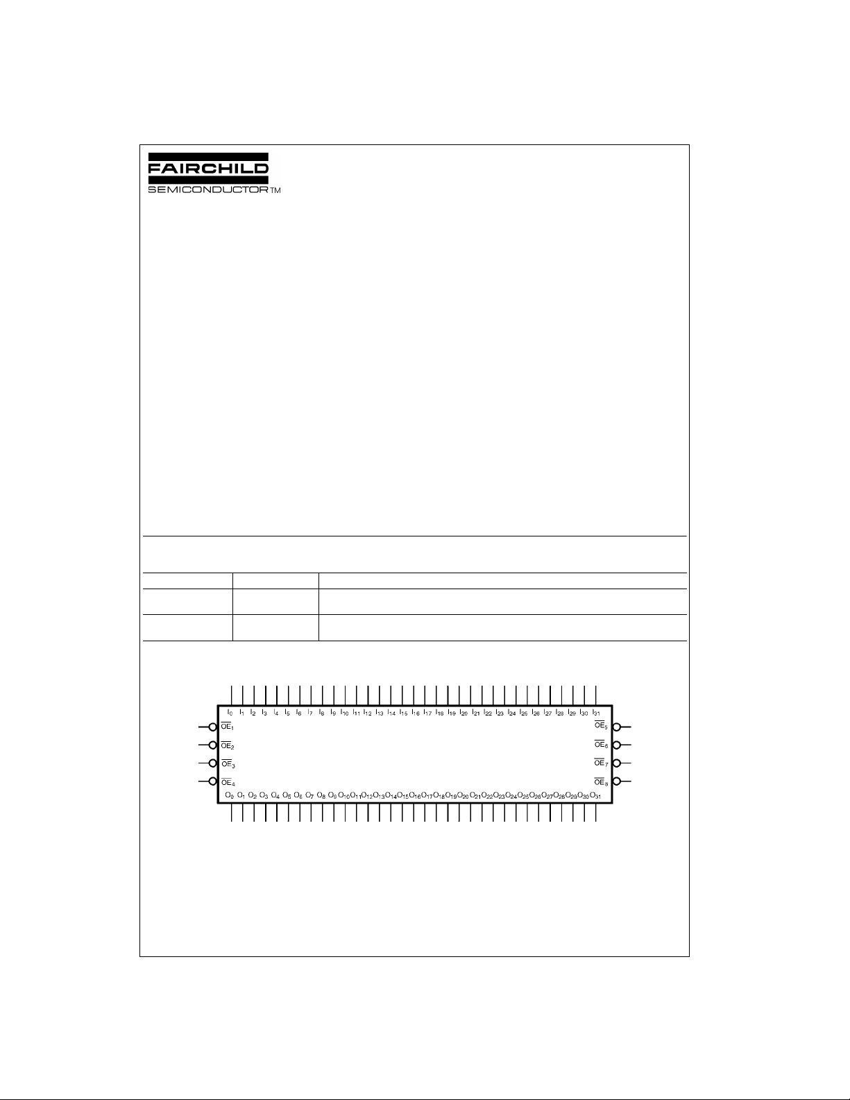
The LVT32244 and LVTH32244 contain thirty-two noninverting buffers with 3-STATE outputs designed to be
employed as a memor y an d ad dr ess d rive r, clock driver, or
bus oriented transm itter /re cei ve r. The device is n ibbl e co ntrolled. Individual 3-STATE control inputs can be shorted
together for 8-bit, 16-bit, or 32-bit operation.
The LVTH32244 data inputs includ e bushold, eliminating
the need for external pull-up resistors to hold unused
inputs.
These buffers and line drivers are designed for low-voltage
(3.3V) V
TTL interface to a 5V environment. The LVT32244 and
LVTH32244 are fabricated with an advanced BiCMOS
technology to achieve high speed ope ration similar to 5V
ABT while maintaining a low power dissipation
applications, but with the capability to provide a
CC
Features
■ Input and output interface capability to systems at
5V V
CC
■ Bushold data inputs eliminate the need for external
pull-up resistors to hold unused inputs (74LVTH32244),
also available without bushold feature (74LVT32244).
■ Live insertion/extraction per mi tt ed
■ Power Up/Down high impedance provides glitch-free
bus loading
■ Outputs source/sink
■ ESD performance:
Human-body model
Machine model
Charged-device model
■ Packaged in plastic Fine-Pitch Ball Grid Array (FBGA)
(Preliminary)
−32 mA/+64 mA
> 2000V
> 200V
Ordering Code:
Order Number Package Number Package Description
74LVT32244GX
(Note 1)
74LVTH32244GX
(Note 1)
Note 1: BGA package available in Tape and Reel only.
BGA96A
(Preliminary)
BGA96A
(Preliminary)
96-Ball Fine-Pitch Ball Grid Array (FBGA), JEDEC MO-205, 5.5mm Wide
[Tape and Reel]
96-Ball Fine-Pitch Ball Grid Array (FBGA), JEDEC MO-205, 5.5mm Wide
[Tape and Reel]
Logic Symbol
> 1000V
© 2001 Fairchild Semiconductor Corporation DS500434 www.fairchildsemi.com
Page 2
Preliminary
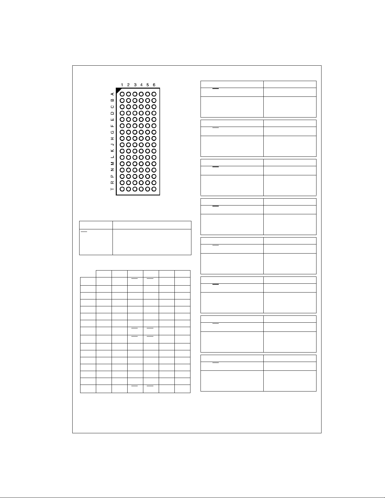
Connection Diagram
74LVT32244 • 74LVTH32244
(Top Thru View)
Pin Descriptions
Pin Names Description
OE
I
0–I31
O
0–O31
n
Output Enable Input (Active LOW)
Inputs
Outputs
Pin Assignments for FBGA
123456
A O
B O3O2GND GND I
C O5O4V
D O7O6GND GND I
E O9O8GND GND I
F O11O10V
G O13O12GND GND I
H O14O15OE4OE3I
J O17O16OE5OE6I
K O19O18GND GND I
L O
M O
N O25O24GND GND I
P O27O26V
R O29O28GND GND I
T O
O0OE1OE2I
1
CC1VCC1I4
CC1VCC1I10I11
21O20VCC2VCC2I20I21
23O22
30O31
GND GND I
CC2VCC2I26I27
OE8OE7I
0
2
6
8
12I13
15I14
16I17
18I19
22I23
24I25
28I29
31I30
Truth Tables
Inputs Outputs
OE
1
LL L
LH H
HX Z
Inputs Outputs
OE
2
LL L
LH H
HX Z
Inputs Outputs
OE
3
LL L
LH H
HX Z
Inputs Outputs
OE
4
LL L
LH H
HX Z
Inputs Outputs
OE
5
LL L
LH H
HX Z
I
1
I
3
I
5
I
7
I
9
H = HIGH Voltage Level
L = LOW Voltage Level
X = Immaterial (HIGH or LOW, inputs may not float)
Z = High Impedance
Inputs Outputs
OE
6
LL L
LH H
HX Z
Inputs Outputs
OE
7
LL L
LH H
HX Z
Inputs Outputs
OE
8
LL L
LH H
HX Z
I0-I
I4-I
I8-I
I12-I
I16-I
I20-I
I24-I
I28-I
3
7
11
15
19
23
27
31
O0-O
O4-O
O8–O
O12-O
O16-O
O20-O
O24-O
O28-O
3
7
11
15
19
23
27
31
www.fairchildsemi.com 2
Page 3

Functional Description
The 74LVT32244 and 74LVTH32244 contain thirty-two
non-inverting bu ffers with 3-STATE outputs. The device is
nibble (4 bits) controlled with each nibble functioning identically, but independent of the other. The contro l pins can be
shorted together to obtain full 32-bit operation. The
Logic Diagrams
Byte 1 Byte 2
Byte 3 Byte 4
Preliminary
3-STATE outputs are controlled by an Output Enable (OE
input. When OE
mode. When OE
high impedance mode but this does not interfere with
entering new data into the inputs.
is LOW, the outputs are in the 2-state
n
is HIGH, the standard o utputs a re in the
n
)
n
74LVT32244 • 74LVTH32244
V
is associated with Bytes 1 and 2.
CC1
is associated with Bytes 3 and 4.
V
CC2
Note: Please note that these diagrams are provided only for the unders t anding of logic operatio ns and should not be used to estimate propagation delays.
3 www.fairchildsemi.com
Page 4

Preliminary
Absolute Maximum Ratings(Note 2)
Symbol Parameter Value Conditions Units
V
CC
V
I
V
O
Supply Voltage −0.5 to +4.6 V
DC Input Voltage −0.5 to +7.0 V
Output Voltage −0.5 to +7.0 Output in 3-STATE
−0.5 to +7.0 Output in High or Low State (Note 3)
I
IK
I
OK
I
O
I
CC
I
GND
74LVT32244 • 74LVTH32244
T
STG
DC Input Diode Current −50 VI < GND mA
DC Output Diode Current −50 VO < GND mA
DC Output Current 64 VO > VCCOutput at HIGH State
128 V
> VCCOutput at LOW State
O
DC Supply Current per Supply Pin ±64 mA
DC Ground Current per Ground Pin ±128 mA
Storage Temperature −65 to +150 °C
Recommended Operating Conditions
Symbol Parameter Min Max Units
V
CC
V
I
I
OH
I
OL
T
A
∆t/∆V Input Edge Rate, V
Note 2: Absolute Maximum continuous ratings are those values beyond which damage to the device may occur. Exposure to these conditions or conditions
beyond those indic ated may adversely affec t device reliability. Functional operation under absolu t e m ax imum rated conditions is not implied.
Absolute Maximum Rating must be observed.
Note 3: I
O
Supply Voltage 2.7 3.6 V
Input Voltage 0 5.5 V
High-Level Output Current −32 mA
Low-Level Output Current 64 mA
Free Air Operating Temperature −40 +85 °C
= 0.8V–2.0V, VCC = 3.0V 0 10 ns/V
IN
V
mA
DC Electrical Characteristics
V
Symbol Parameter
V
IK
V
IH
V
IL
V
OH
V
OL
I
I(HOLD)
(Note 4) −75 VI = 2.0V
I
I(OD)
(Note 4) Current to Change State −500 (Note 6)
I
I
I
OFF
I
PU/PD
I
OZL
I
OZH
I
OZH
Input Clamp Diode Voltage 2.7 −1.2 V II = −18 mA
Input HIGH Voltage 2.7–3.6 2.0 V VO ≤ 0.1V or
Input LOW Voltage 2.7–3.6 0.8 V VO ≥ VCC − 0.1V
Output HIGH Voltage 2.7–3.6 VCC − 0.2
Output LOW Voltage 2.7 0.2
Bushold Input Minimum Drive 3.0 75
Bushold Input Over-Drive 3.0 500
Input Current 3.6 10
Control Pins 3.6 ±1V
Data Pins 3.6
Power Off Leakage Current 0 ±100 µA0V ≤ VI or VO ≤ 5.5V
Power Up/Down
3-STATE Current VI = GND or V
3-STATE Output Leakage Current 3.6 −5 µAVO = 0.5V
3-STATE Output Leakage Current 3.6 5 µAVO = 3.0V
+ 3-STATE Output Leakage Current 3.6 10 µAVCC < VO ≤ 5.5V
CC
(V) Min Max
2.7 2.4 I
3.0 2.0 IOH = −32 mA
2.7 0.5 I
3.0 0.4 IOL = 16 mA
3.0 0.5 IOL = 32 mA
3.0 0.55 IOL = 64 mA
0 – 1.5V ±100 µA
TA = −40°C to +85°C
−5V
1V
Units Conditions
IOH = −100 µA
V
V
µA
µA
µA
= −8 mA
OH
IOL = 100 µA
= 24 mA
OL
VI = 0.8V
(Note 5)
VI = 5.5V
= 0V or V
I
= 0V
I
= V
I
CC
VO = 0.5V to 3.0V
CC
CC
www.fairchildsemi.com 4
Page 5

DC Electrical Characteristics (Continued)
Preliminary
74LVT32244 • 74LVTH32244
V
Symbol Parameter
I
CCH
I
CCL
I
CCZ
I
CCZ
∆I
Note 4: Applies t o bushold versions only (LVTH32244).
Note 5: An external driver must source at least the specified current to switch from LOW-to-HIGH.
Note 6: An external driver must sink at least the specified current to switch from HIGH-to-LOW.
Note 7: This is the increase in supply c urrent for each input that is at the specified volt age level rather than V
Power Supply Current V
Power Supply Current V
Power Supply Current V
+ Power Supply Current V
Increase in Power Supply Current 3.6 0.2 mA One Input at VCC − 0.6V
CC
(Note 7) V
CC1
CC1
CC1
CC1
CC1
or V
or V
or V
or V
or V
CC2
CC2
CC2
CC2
CC2
CC
(V) Min Max
3.6 0.19 mA Outputs High
3.6 5.0 mA Outputs Low
3.6 0.19 mA Outputs Disabled
3.6 0.19 mA VCC ≤ VO ≤ 5.5V,
TA = −40°C to +85°C
Dynamic Switching Characteristics (Note 8)
V
Symbol Parameter
V
OLP
V
OLV
Note 8: Characterized in SSOP package. Guaranteed parameter, but not tested.
Note 9: Max number of outputs defined as (n). n−1 data inputs are driven 0V to 3V. Output under test held LOW.
Quiet Output Maximum Dynamic V
Quiet Output Minimum Dynamic V
OL
CC
(V) Min Typ Max
3.3 0.8 V (Note 9)
OL
3.3 −0.8 V (Note 9)
TA = 25°C
AC Electrical Characteristics
TA = −40°C to +85°C
Symbol Parameter
t
t
t
t
t
t
PLH
PHL
PZH
PZL
PHZ
PLZ
Propagation Delay Data to Output 1.2 3.5 1.2 3.9
Output Enable Time 1.2 4.0 1.2 5.0
Output Disable Time 2.0 4.7 2.0 5.2
CL = 50 pF, RL = 500Ω
VCC = 3.3V ± 0.3V VCC = 2.7V
Min Max Min Max
1.2 3.5 1.2 3.9
1.2 5.0 1.2 6.5
1.5 4.2 1.5 4.4
Units Conditions
Outputs Disabled
Other Inputs at VCC or GND
or GND.
CC
Units
CL = 50 pF, RL = 500Ω
Conditions
Units
ns
ns
ns
Capacitance
(Note 10)
Symbol Parameter Conditions Typical Units
C
IN
C
OUT
Note 10: Capacita nc e is m easured at frequency f = 1 MHz, per MIL-STD -883, Method 3012.
Input Capacitance VCC = 0V, VI = 0V or V
Output Capacitance VCC = 3.0V, VO = 0V or V
CC
CC
4pF
8pF
5 www.fairchildsemi.com
Page 6

Physical Dimensions inches (millimeters) unless otherwise noted
Preliminary
96-Ball Fine-Pitch Ball Grid Array (FBGA), JEDEC MO-205, 5.5mm Wide
Fairchild does not assume any responsibility for use of any circuitr y described, no circuit patent licenses are implied a nd
Fairchild reserves the right at any time without notice to change said circuitry and specifications.
LIFE SUPPORT POLICY
FAIRCHILD’S PRODUCTS ARE NOT AUTHORIZED FOR USE AS CRITICAL COMPONENTS IN LIFE SUPPORT
DEVICES OR SYSTEMS WITHOUT THE EXPRESS WRITTEN APPROVAL OF THE PRESIDENT OF FAIRCHILD
SEMICONDUCTOR CORPORATION. As used herein:
1. Life support devices or systems are device s or syste ms
74LVT32244 • 74LVTH32244 Low Voltage 32-Bit Buffer/Line Driver with 3-STATE Outputs (Preliminary)
which, (a) are intended for surgical implant into the
body, or (b) support or sustain life, and (c) whose failure
to perform when properly used in accordance with
instructions for use provided in the labeling, can be reasonably expected to result in a significant inju ry to the
user.
www.fairchildsemi.com 6
Package Number BGA96A
Preliminary
2. A critical component in any compon ent of a l ife supp ort
device or system whose failu re to perform can be reasonably expected to cause the failure of the li fe su pp ort
device or system, or to affect its safety or effectiveness.
www.fairchildsemi.com
 Loading...