

Datasheet 74LVTH245WMX, 74LVTH245WM, 74LVTH245SJX, 74LVTH245SJ, 74LVTH245MTC Datasheet (Fairchild Semiconductor)
...Page 1
74LVT245 • 74LVTH245
Low Voltage Octal B idirectional Transceiver
with 3-STATE Inputs/Outputs
74LVT245 • 74LVTH245 Low Voltage Octal Bidirectional Transceiver with 3-STATE Inputs/Outputs
November 1999
Revised January 2000
General Description
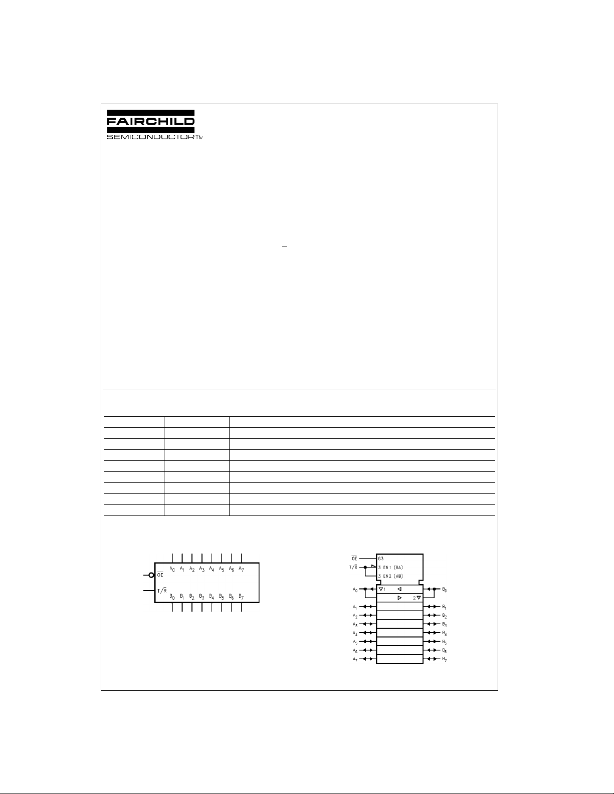
The LVT245 and LVTH245 contain eight non-inverting bidirectional buffers with 3-STATE outputs and are intended for
bus-oriented applications. The Transmit/Receive (T/R
input determines the direction of data flow through the bidirectional transceive r. Transmit (active-HIGH) enable s data
from A ports to B ports; Receive (active-LOW) enables
data from B ports to A ports. The Output Enable input,
when HIGH, disables both A and B ports by placing them in
a HIGH Z condition.
The LVTH245 data inputs inclu de bushold, el iminating the
need for external pull-up resistors to hold unused inputs.
These transceivers are designed for low-voltage (3.3V)
applications, bu t with the capabi lity to provide a TTL
V
CC
interface to a 5V environm ent. The LVT245 an d LVTH245
are fabricated with an advanced BiCMOS technology to
achieve high speed operation similar to 5V ABT while
maintaining a low power dissipation.
Features
■ Input and output interface capability to systems at
5V V
)
CC
■ Bushold data inputs el iminate th e need fo r exter nal pullup resistors to hold unused inpu ts (74LVTH245), also
available without bushold feature (74LVT245).
■ Live insertion/extraction permitted
■ Power Up/Down high impedance provides glitch-free
bus loading
■ Outputs source /sink, −32 mA/+64 mA
■ Latch-up performance exceeds 500 mA
Ordering Code:
Order Number Package Number Package Description
74LVT245WM M20B 20-Lead Small Outline Integrated Circuit (SOIC), JEDEC MS-013, 0.300” Wide
74LVT245SJ M20D 20-Lead Small Outline Package (SOP), EIAJ TYPE II 5.3mm Wide
74LVT245MSA MSA20 20-Lead Shrink Small Outline Package (SSOP), EIAJ TYPE II, 5.3mm Wide
74LVT245MTC MTC20 20-Lead Thin Shrink Small Outline Package (TSSOP), JEDEC MO-153, 4.4mm Wide
74LVTH245WM M20B 20-Lead Small Outline Integrated Circuit (SOIC), JEDEC MS-013, 0.300” Wide
74LVTH245SJ M20D 20-Lead Small Outline Package (SOP), EIAJ TYPE II 5.3mm Wide
74LVTH245MSA MSA20 20-Lead Shrink Small Outline Package (SSOP), EIAJ TYPE II, 5.3mm Wide
74LVTH245MTC MTC20 20-Lead Thin Shrink Small Outline Package (TSSOP), JEDEC MO-153, 4.4mm Wide
Device also availabl e in Tape and Reel. Specify by appending suffix letter “X” to the ordering code.
Logic Symbols
IEEE/IEC
© 2000 Fairchild Semiconductor Corporation DS500203 www.fairchildsemi.com
Page 2
Connection Diagram Pin Descriptions
Pin Names Description
OE
T/R
A
B
0–A7
0–B7
Output Enable Input
Transmit/Receive Input
Side A Inputs or 3-STATE Outputs
Side B Inputs or 3-STATE Outputs
Truth Table
74LVT245 • 74LVTH245
H = HIGH Voltage Level
L = LOW Voltage Level
X = Immaterial
Inputs
OE
L L Bus B Data to Bus A
L H Bus A Data to Bus B
HXHIGH-Z State
T/R
Outputs
www.fairchildsemi.com 2
Page 3
Absolute Maximum Ratings(Note 1)
Symbol Parameter Value Conditions Units
V
CC
V
I
V
O
Supply Voltage −0.5 to +4.6 V
DC Input Voltage −0.5 to +7.0 V
Output Voltage −0.5 to +7.0 Output in 3-STATE V
−0.5 to +7.0 Output in HIGH or LOW State (Note 2) V
I
I
I
I
I
T
IK
OK
O
CC
GND
STG
DC Input Diode Current −50 VI < GND mA
DC Output Diode Current −50 VO < GND mA
DC Output Current 64 VO > VCCOutput at HIGH State
128 V
> VCCOutput at LOW State
O
DC Supply Current per Supply Pin ±64 mA
DC Ground Current per Ground Pin ±128 mA
Storage Temperature −65 to +150 °C
Recommended Operating Conditions
Symbol Parameter Min Max Units
V
CC
V
I
I
OH
I
OL
T
A
∆t/∆V Input Edge Rate, V
Note 1: Absolute Maximum continuous ratings are those values beyond which damage to the device may occur. Exposure to these conditions or conditions
beyond those indicated may adversely affect device reliability. Functional operation under absolute maximum rated conditions is not implied.
Note 2: I
Supply Voltage 2.7 3.6 V
Input Voltage 0 5.5 V
High-Level Output Current −32 mA
Low-Level Output Current 64 mA
Free Air Operating Temperature −40 +85 °C
= 0.8V–2.0V, VCC = 3.0V 0 10 ns/V
IN
Absolute Maximum Rating must be observed.
O
74LVT245 • 74LVTH245
mA
DC Electr ic al C h ar acteristi cs
V
TA = −40°C to +85°C
Symbol Parameter
V
IK
V
IH
V
IL
V
OH
V
OL
I
I(HOLD)
(Note 3) −75 µAVI = 2.0V
I
I(OD)
(Note 3) Current to Change State −500 µA (Note 5)
I
I
I
OFF
I
PU/PD
I
OZL
I
OZL
I
OZH
Input Clamp Diode Voltage 2.7 −1.2 V II = −18 mA
Input HIGH Voltage 2.7–3.6 2.0
Input LOW Voltage 2.7–3.6 0.8 VO ≥ VCC − 0.1V
Output HIGHVoltage 2.7–3.6 VCC - 0.2 V IOH = −100 µA
Output LOW Voltage 2.7 0.2 V IOL = 100 µA
Bushold Input Minimum Drive 3.0 75 µAVI = 0.8V
Bushold Input Over-Drive 3.0 500 µA (Note 4)
Input Current 3.6 10 µAVI = 5.5V
Control Pins 3.6 ±1 µAVI = 0V or V
Data Pins 3.6 −5 µAVI = 0V
Power Off Leakage Current 0 ±100 µA0V ≤ VI or VO ≤ 5.5V
Power Up/Down
3-STATE Current VI = GND to V
3-STATE Output Leakage Current 3.6 −5 µAVO = 0.5V
(Note 3) 3-STATE Output Leakage Current 3.6 −5 µAVO = 0.0V
3-STATE Output Leakage Current 3.6 5 µAVO = 3.0V
CC
(V) Min Max
2.7 2.4 V IOH = − 8 mA
3.0 2.0 V IOH = −32 mA
2.7 0.5 V IOL = 24 mA
3.0 0.4 V IOL = 16 mA
3.0 0.5 V IOL = 32 mA
3.0 0.55 V IOL = 64 mA
0–1.5V ±100 µA
Units Conditions
VO ≤ 0.1V or
V
1 µAVI = V
VO = 0.5V to V
CC
CC
CC
CC
3 www.fairchildsemi.com
Page 4

DC Electrical Characteristics (Continued)
V
TA = −40°C to +85°C
Symbol Parameter
I
(Note 3) 3-STATE Output Leakage Current 3.6 5 µAVO = 3.6V
OZH
I
+ 3-STATE Output Leakage Current 3.6 10 µAVCC < VO ≤ 5.5V
OZH
I
I
I
I
CCH
CCL
CCZ
CCZ
Power Supply Current 3.6 0.19 mA Outputs HIGH
Power Supply Current 3.6 5 mA Outputs LOW
Power Supply Current 3.6 0.19 mA Outputs Disabled
+ Power Supply Current
74LVT245 • 74LVTH245
∆I
CC
Note 3: Applies to B ushold versions only (LVTH245).
Note 4: An external driver must source at least the specified current to switch from LOW-to-HIGH.
Note 5: An external driver must sink at least the specified current to switch from HIGH-to-LOW.
Note 6: This is the increase in supply current for each input that is at the specified voltage level rather than V
Increase in Power Supply Current
(Note 6) Other Inputs at VCC or GND
CC
(V) Min Max
Units Conditions
3.6 0.19 mA
3.6 0.2 mA
or GND.
CC
VCC ≤ VO ≤ 5.5V,
Outputs Disabled
One Input at VCC − 0.6V
Dynamic Switching Characteristics (Note 7)
V
Symbol Parameter
V
OLP
V
OLV
Note 7: Characterized in SOIC pac kage. Guaranteed parameter, but not tested.
Note 8: Max number of outputs defined as (n). n−1 data inputs are driven 0V to 3V. Output under test held LOW.
Quiet Output Maximum Dynamic V
Quiet Output Minimum Dynamic V
OL
OL
CC
(V)
3.3 0.8 V (Note 8)
3.3 −0.8 V (Note 8)
TA = 25°C
Min Typ Max
Units
Conditions
CL = 50 pF,
RL = 500Ω
AC Electrical Characteristics
TA = −40°C to +85°C
Symbol Parameter
VCC = 3.3V ± 0.3V VCC = 2.7V
Min Max Min Max
t
PLH
t
PHL
t
PZH
t
PZL
t
PHZ
t
PLZ
t
OSHL
t
OSLH
Note 9: Skew is defined as the absolute value of the difference between the actual propagation delay for any two separate outputs of the same device. The
specifi cation applies to any outputs switching in the same direction, either HIGH-to-LOW (t
Propagation Delay 1.2 3.6 1.2 4.0
1.23.51.24.0
Output Enable Time 1.3 5.5 1.3 7.1
1.75.71.76.7
Output Disable 2.0 5.9 2.0 6.5
2.05.02.05.1
Output to Output Skew
(Note 9)
CL = 50 pF, RL = 500Ω
1.0 1.0 ns
) or LOW-to-HIGH (t
OSHL
OSLH
).
Units
ns
ns
ns
Capacitance (Note 10)
Symbol Parameter Conditions Typical Units
C
IN
C
I/O
Note 10: Capacitance is meas ured at frequency f = 1 MHz, per MIL-STD-883, Method 3012.
www.fairchildsemi.com 4
Input Capacitance VCC = 0V, VI = 0V or V
Input/Output Capacitance VCC = 3.0V, VO = 0V or V
CC
CC
4pF
8pF
Page 5

Physical Dimensions inches (millimeters) unless otherwise noted
74LVT245 • 74LVTH245
20-Lead Small Outline Integrated Circuit (SOIC), JEDEC MS-013, 0.300” Wide
20-Lead Small Outline Package (SOP), EIAJ TYPE II 5.3mm Wide
Package Number M20B
Package Number M20D
5 www.fairchildsemi.com
Page 6

Physical Dimensions inches (millimeters) unless otherwise noted (Continued)
74LVT245 • 74LVTH245
20-Lead Shrink Small Outline Package (SSOP), EIAJ TYPE II, 5.3mm Wide
Package Number MSA20
www.fairchildsemi.com 6
Page 7

Physical Dimensions inches (millimeters) unless otherwise noted (Continued)
74LVT245 • 74LVTH245 Low Voltage Octal Bidirectional Transceiver with 3-STATE Inputs/Outputs
20-Lead Thin Shrink Small Outline Package (TSSOP), JEDEC MO-153, 4.4mm Wide
Fairchild does not a ssume any res ponsibility f or use of any circuitry descri bed, no circ uit patent li censes are im plied and
Fairchild reserves the right at any time without notice to change said circuitry and specifications.
LIFE SUPPORT POLICY
FAIRCHILD’S PRODUCTS ARE NOT AUTHORIZED FOR USE AS CRITICAL COMPONENTS IN LIFE SUPPORT
DEVICES OR SYSTEMS WITHOUT THE EXPRESS WRITTEN APPROVAL OF THE PRESIDENT OF FAIRCHILD
SEMICONDUCTOR CORPORATION. As used herein:
1. L ife suppor t devices or systems are devic es or systems
which, (a) are intended for surgical implant into the
body, or (b) support or sustain life, and (c) whose failure
to perform when properly used in accordance with
instructions for use provided in the labeling, can be reasonably expect ed to result in a si gnificant injury to the
user.
Package Number MTC20
2. A critical component i n an y comp onent of a l ife suppor t
device or system whose failur e to perform can be reasonably expected to cause the fai lure of the life sup port
device or system, or to affect its safety or effectiveness.
www.fairchildsemi.com
7 www.fairchildsemi.com
 Loading...