

Datasheet 74LVTH16652MTDX, 74LVTH16652MTD, 74LVTH16652MEAX, 74LVTH16652MEA Datasheet (Fairchild Semiconductor)
Page 1
© 2000 Fairchild Semiconductor Corporation DS012024 www.fairchildsemi.com
January 2000
Revised January 2000
74LVTH16652 Low Voltage 16-Bit Transceiver/Register with 3-STATE Outputs
74LVTH16652
Low Voltage 16-Bit Transceiver/Register
with 3-STATE Outputs
General Description
The LVTH16652 consists of sixteen bus transceiver circuits
with D-type flip-flops, and control circuitry arranged for multiplexed transmission of data direct ly from the input bus or
from the internal registers. Each byte has separate control
inputs which can be shorte d together for full 16-bit operation. Data on the A or B bus will be clocked into the registers as the appropriat e clock pin goes to the HIGH logic
level. Output Enable pins (OEAB, OEBA
) are provided to
control the transceiver function (see Functional Description).
The LVTH16652 data inputs includ e bushold, eliminating
the need for external pull-up resistors to hold unused
inputs.
The transceivers are d esigned for low-volta ge (3.3V) V
CC
applications, but with the capability to provide a TTL interface to a 5V environment. The LVTH16652 is fab ricated
with an advanced BiCMOS technology to achieve high
speed operation similar to 5V ABT while maintaining low
power dissipation.
Features
■ Input and output interface capability to systems at
5V V
CC
■ Bushold data inputs eliminate the need for external
pull-up resistors to hold unused inputs
■ Live insertion/extraction per mitt ed
■ Power Up/Down high impedance provides glitch-free
bus loading
■ Outputs source/sink −32 mA/+64 mA
■ Functionally compatible with the 74 series 16652
■ Latch-up performance exceeds 500 mA
Ordering Code:
Devices also availab le in Tape and Reel. Specify by appending su ffix let te r “X” to the ordering code.
Order Number Package Number Package Description
74LVTH16652MEA MS56A 56-Lead Shrink Small Outline Package (SSOP), JEDEC MO-118, 0.300 Wide
74LVTH16652MTD MTD56 56-Lead Thin Shrink Small Outline Package (TSSOP), JEDEC MO-153, 6.1mm Wide
Page 2
www.fairchildsemi.com 2
74LVTH16652
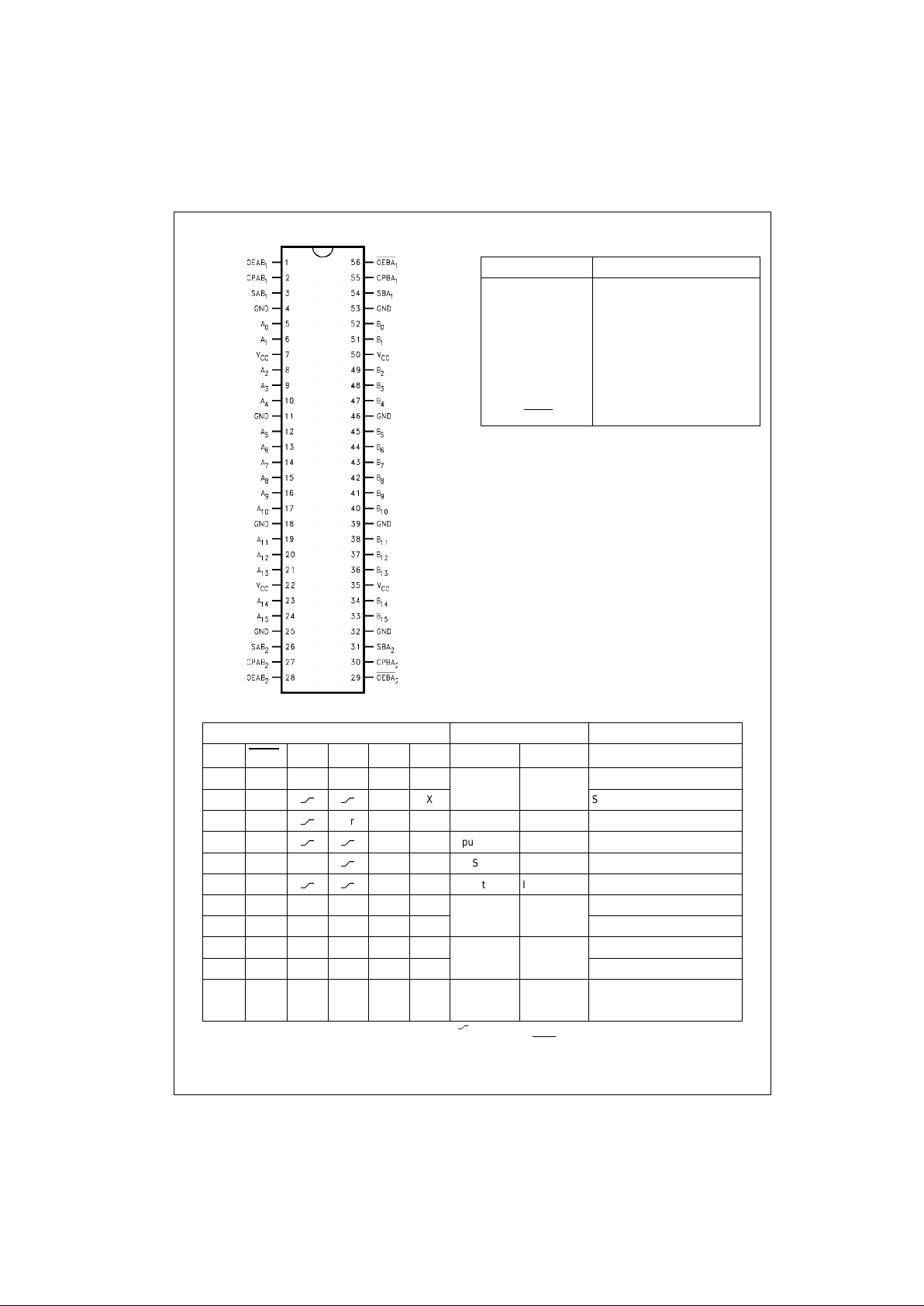
Connection Diagram Pin Descriptions
Truth Table
(Note 1)
H = HIGH Voltage Level L = LOW Voltage Lev el X = Immaterial = LOW-to-HIGH Clock Transition
Note 1: The data output fu nction s may b e enable d or di sabled b y variou s signa ls at OEA B or O EBA
inputs. Data input function s are a lways e nabled, i.e.,
data at the bus pins w ill be stored on every LOW- to -H I GH t ransition on the clock inp ut s . This also applies to data I/O (A and B: 8–15) and #2 cont rol pins
Pin Names Description
A
0–A15
Data Register A Inputs/
3-STATE Outputs
B
0–B15
Data Register B Inputs/
3-STATE Outputs
CPAB
n
, CPBA
n
Clock Pulse Inputs
SAB
n
, SBA
n
Select Inputs
OEAB
n
, OEBA
n
Output Enable Inputs
Inputs Inputs/Outputs Operating Mode
OEAB
1
OEBA1CPAB1CPBA1SAB1SBA1A0 thru A7B0 thru B
7
L H H or L H or L X X Input Input Isolation
LH
X X Store A and B Data
XH
H or L X X Input Not Specified Store A, Hold B
HH
X X Input Output Store A in Both Registers
LXH or L
X X Not Specified Input Hold A, Store B
LL
X X Output Input Store B in Both Registers
L L X X X L Output Input Real-Time B Data to A Bus
L L X H or L X H Store B Data to A Bus
H H X X L X Input Output Real-Time A Data to B Bus
H H H or L X H X Stored A Data to B Bus
H L H or L H or L H H Output Output Stored A Data to B Bus and
Stored B Data to A Bus
Page 3
3 www.fairchildsemi.com
74LVTH16652
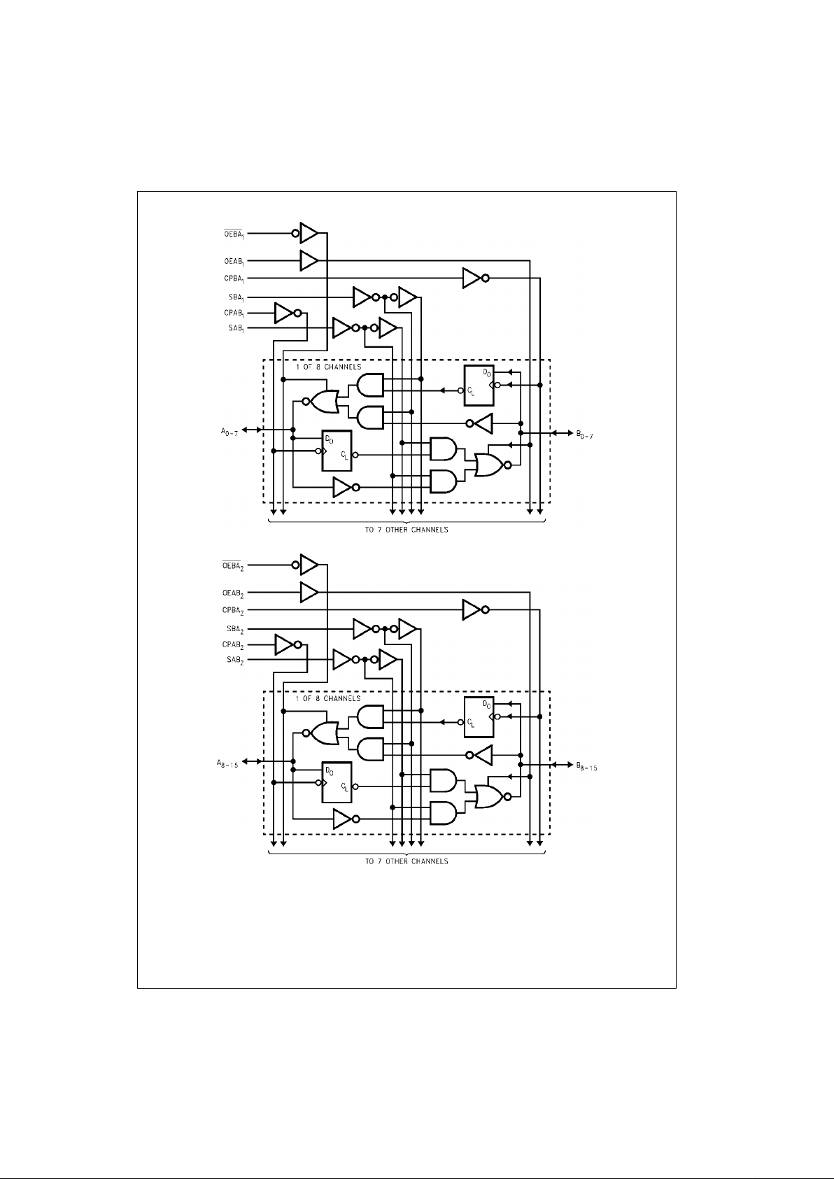
Logic Diagrams
Please note that thes e diagrams are provide d only for the understan ding of logic operations a nd should not be used to es t im ate propagation delays.
Page 4

www.fairchildsemi.com 4
74LVTH16652
Functional Description
In the transceiver mo de, data prese nt at the HIGH im pedance port may be stored in either the A or B register or
both.
The select (SAB
n
, SBAn) controls can multiplex sto red an d
real-time.
The examples below demonstrate the four fundamental
bus-management func tions that can be perfor med wi th the
LVTH16652.
Data on the A or B data bus, or both can be stored in the
internal D flip-flop by LOW-to-HIGH transitions at the
appropriate Clock Inputs (CPAB
n
, CPBAn) regardless of
the Select or Output Ena ble Inputs. When SAB and SBA
are in the real time transfer mode, it is also possible to
store data without using the internal D flip-flops by simultaneously enabling OE AB
n
and OEBAn. In this configuration
each Output reinfor ces its Input. T hus when all other data
sources to the two sets of bus lines are in a HIGH impedance state, each set of bus lines will remain at its last state.
Real-Time Transfer
Bus B to Bus A
Storage
Real-Time Transfer
Bus A to Bus B
Transfer Storage
Data to A or B
OEAB
1
OEBA1CPAB1CPBA1SAB1SBA
1
LLXXXL
OEAB1OEBA1CPAB1CPBA1SAB1SBA
1
XH
XXX
LXX
XX
LH
XX
OEAB1OEBA1CPAB1CPBA1SAB1SBA
1
HHXXLX
OEAB1OEBA1CPAB1CPBA1SAB1SBA
1
HLH or LH or LHH
Page 5

5 www.fairchildsemi.com
74LVTH16652
Absolute Maximum Ratings(Note 2)
Recommended Operating Conditions
Note 2: Absolute Maximum continuous ratings are those values beyond which damage to the device may occur. Exposure to these conditions or conditions
beyond those indica te d m ay adversely affect dev ic e reliability. Functional operation under absolute maxim um rated conditions is not imp lied.
Note 3: I
O
Absolute Maximum Rating must be observed.
Symbol Parameter Value Conditions Units
V
CC
Supply Voltage −0.5 to +4.6 V
V
I
DC Input Voltage −0.5 to +7.0 V
V
O
DC Output Voltage −0.5 to +7.0 Output in 3-STATE
V
−0.5 to +7.0 Output in HIGH or LOW State (Note 3)
I
IK
DC Input Diode Current −50 VI < GND mA
I
OK
DC Output Diode Current −50 VO < GND mA
I
O
DC Output Current 64 VO > VCCOutput at HIGH State
mA
128 V
O
> VCCOutput at LOW State
I
CC
DC Supply Current per Supply Pin ±64 mA
I
GND
DC Ground Cu rrent per Ground Pin ±128 mA
T
STG
Storage Temperature −65 to +150 °C
Symbol Parameter Min Max Units
V
CC
Supply Voltage 2.7 3.6 V
V
I
Input Voltage 0 5.5 V
I
OH
HIGH-Level Output Current −32 mA
I
OL
LOW-Level Output Current 64 mA
T
A
Free-Air Operating Temperature −40 85 °C
∆t/∆V Input Edge Rate, V
IN
= 0.8V–2.0V, VCC = 3.0V 0 10 ns/V
Page 6

www.fairchildsemi.com 6
74LVTH16652
DC Electrical Characteristics
Note 4: An externa l driv er must source at leas t the specified current to s w it c h f rom LOW-to-HIGH.
Note 5: An externa l driv er must sink at least the sp ec if ied current to switch from H I GH-to-LOW.
Note 6: This is the increase in supply current f or each input that is at the spe c if ied voltage level rather t han V
CC
or GND.
Dynamic Switching Characteristics (Note 7)
Note 7: Characteriz ed in SOIC package. Guaranteed parameter, but not tes t ed.
Note 8: Max number of outputs defined a s (n ). n−1 data inputs are driven 0V to 3V. Output under test held LOW.
Symbol Parameter
T A = −40°C to +85°C
Units ConditionsV
CC
Min Max
(V)
V
IK
Input Clamp Diode Voltage 2.7 −1.2 V II = −18 mA
V
IH
Input HIGH Voltage 2.7–3.6 2.0 V VO ≤ 0.1V or
VO ≥ VCC − 0.1V
V
IL
Input LOW Voltage 2.7–3.6 0.8 V
V
OH
Output HIGH Voltage 2.7–3.6 VCC − 0.2
V
IOH = −100 µA
2.7 2.4 IOH = −8 mA
3.0 2.0 IOH = −32 mA
V
OL
Output LOW Voltage 2.7 0.2
V
IOL = 100 µA
2.7 0.5 IOL = 24 mA
3.0 0.4 IOL = 16 mA
3.0 0.5 IOL = 32 mA
3.0 0.55 IOL = 64 mA
I
I(HOLD)
Bushold Input Minimum Drive 3.0 75
µA
VI = 0.8V
−75 VI = 2.0V
I
I(OD)
Bushold Input Over-Drive 3.0 500
µA
(Note 4)
Current to Change State −500 (Note 5)
I
I
Input Current 3.6 10
µA
VI = 5.5V
Control Pins 3.6 ±1V
I
= 0V or V
CC
Data Pins 3.6 −5V
I
= 0V
1V
I
= V
CC
I
OFF
Power Off Leakage Current 0 ±100 µA0V ≤ VI or VO ≤ 5.5V
I
PU/PD
Power up/down 3-STATE 0–1.5V ±100 µAVO = 0.5V to 3.0V
Output Current VI = GND or V
CC
I
OZL
3-STATE Output Leakage Current 3.6 −5 µAVO = 0.0V
I
OZH
3-STATE Output Leakage Current 3.6 5 µAVO = 3.6V
I
OZH
+ 3-STATE Output Leakage Current 3.6 10 µAVCC < VO ≤ 5.5V
I
CCH
Power Supply Current 3.6 0.19 mA Outputs HIGH
I
CCL
Power Supply Current 3.6 5 mA Outputs LOW
I
CCZ
Power Supply Current 3.6 0.19 mA Outputs Disabled
I
CCZ
+ Power Supply Current 3.6 0.19 mA VCC ≤ VO ≤ 5.5V,
Outputs Disabled
∆I
CC
Increase in Power Supply Current 3.6 0.2 mA One Input at VCC − 0.6V
(Note 6) Other Inputs at VCC or GND
Symbol Parameter
V
CC
(V)
TA = 25°C
Units
Conditions
CL = 50 pF
RL = 500Ω
Min Typ Max
V
OLP
Quiet Output Maximum Dynamic V
OL
3.3 0.8 V (Note 8)
V
OLV
Quiet Output Minimum Dynamic V
OL
3.3 −0.8 V (Note 8)
Page 7

7 www.fairchildsemi.com
74LVTH16652
AC Electrical Characteristics
Note 9: Skew is def ined as the absol ut e v alue of the difference between the actu al propagation del ay f or any two separate outputs of the same device. The
specification applies t o any outputs switching in the same direction, ei th er HIGH-to-LOW (t
OSHL
) or LOW-to-HIGH (t
OSLH
).
Capacitance (Note 10)
Note 10: Capacitanc e is m easured at frequency f = 1 MHz, per MIL-STD-883, Method 3012.
Symbol Parameter
TA = −40°C to +85°C
Units
CL = 50 pF, RL = 500Ω
VCC = 3.3V ± 0.3V VCC = 2.7V
Min Max Min Max
f
MAX
Maximum Clock Frequency 150 150 MHz
t
PHL
Propagation Delay 1.3 4.8 1.3 5.4
ns
t
PLH
CPAB or CPBA to A or B 1.3 5.1 1.3 5.6
t
PHL
Propagation Delay 1.0 4.5 1.0 5.1
ns
t
PLH
Data to A or B 1.0 4.4 1.0 4.7
t
PHL
Propagation Delay 1.0 4.9 1.0 5.5
ns
t
PLH
SBA or SAB to A or B 1.0 4.8 1.0 5.4
t
PZL
Output Enable Time 1.0 4.9 1.0 5.8
ns
t
PZH
OE to A
1.04.81.05.8
t
PLZ
Output Disable Time 1.6 5.6 1.6 6.1
ns
t
PHZ
OE to A
2.05.42.06.1
t
PZL
Output Enable Time 1.3 5.0 1.3 5.4
ns
t
PZH
OE to B 1.3 4.8 1.3 5.4
t
PLZ
Output Disable Time 1.3 5.5 1.3 6.2
ns
t
PHZ
OE to B 1.3 5.6 1.3 6.3
t
S
Setup Time A or B before CPAB or CPBA, Data HIGH 1.2 1.5
ns
A or B before CPAB or CPBA, Data LOW 2.0 2.8
t
H
Hold Time A or B before CPAB or CPBA, Data HIGH 0.5 0.0
ns
A or B before CPAB or CPBA, Data LOW 0.5 0.5
t
W
Pulse Width CPAB or CPBA HIGH or LOW 3.3 3.3 ns
t
OSHL
Output to Output Skew (Note 9) 1.0 1.0
ns
t
OSLH
1.0 1.0
Symbol Parameter Conditions Typical Units
C
IN
Input Capacitance VCC = Open, VI = 0V or V
CC
4pF
C
I/O
Input/Output Capacitance VCC = 3.0V, VO = 0V or V
CC
8pF
Page 8

www.fairchildsemi.com 8
74LVTH16652
Physical Dimensions inches (millimeters) unless otherwise noted
56-Lead Shrink Small Outline Package (SSOP), JEDEC MO-118, 0.300 Wide
Package Number MS56A
Page 9

9 www.fairchildsemi.com
74LVTH16652 Low Voltage 16-Bit Transceiver/Register with 3-STATE Outputs
Physical Dimensions inches (millimeters) unless otherwise noted (Continued)
56-Lead Thin Shrink Small Outline Package (TSSOP), JEDEC MO-153, 6.1mm Wide
Package Number MTD56
Fairchild does not assume any responsibility for use of any circu itry described, no circuit patent license s are implied and
Fairchild reserves the right at any time without notice to change said circuitry and specifications.
LIFE SUPPORT POLICY
FAIRCHILD’S PRODUCTS ARE NOT AUTHORIZED FOR USE AS CRITICAL COMPONENTS IN LIFE SUPPORT
DEVICES OR SYSTEMS WITHOUT THE EXPRESS WRITTEN APPROVAL OF THE PRESIDENT OF FAIRCHILD
SEMICONDUCTOR CORPORATION. As used herein:
1. Life support devices or systems are dev ic es or syste ms
which, (a) are intended for surgical implant into the
body, or (b) support or sustain life, and (c) whose failure
to perform when properly used in accordance with
instructions for use provided i n the labe li ng, can be re asonably expected to result in a significant injury to the
user.
2. A critical component in any com ponen t of a life s uppor t
device or system whose failu re to perform can b e reasonably expected to c ause th e fa i lure of the li fe s upp or t
device or system, or to affect its safety or effectiveness.
www.fairchildsemi.com
 Loading...