

Datasheet 74LVTH32374GX, 74LVTH16374MTDX, 74LVTH16374MTD, 74LVTH16374MEAX, 74LVTH16374MEA Datasheet (Fairchild Semiconductor)
Page 1
January 1999
Revised April 1999
74LVT16374 • 74LVTH16374 Low Voltage 16-Bit D-Type Flip-Flop with 3-STATE Outputs
© 1999 Fairchild Semiconductor Corporation DS012022.prf www.fairchildsemi.com
74LVT16374 • 74LVTH16374
Low Voltage 16-Bit D-Type Flip-Flop with
3-STATE Outputs
General Description
The LVT16374 and LVTH16374 contain sixteen non-inverting D-type flip-flops with 3-STATE outputs and is intended
for bus oriented applications. The device is byte controlled.
A buffered clock (CP) and Output Enable ( OE
) are common to each byte and can be shorted together for full 16-bit
operation.
The LVTH16374 data inputs includ e bushold, eliminating
the need for external pull-up resistors to hold unused
inputs.
These flip-flops are de signed for low-voltage (3.3V) V
CC
applications, but with the capability to provide a TTL interface to a 5V environment. Th e LVT16374 and LVTH16374
are fabricated with an advanced BiCMOS technology to
achieve high speed operation similar to 5V ABT while
maintaining a low power dissipation.
Features
■ Input and output interface capa bility to systems at 5V
V
CC
■ Bushold data inputs elimina te the nee d for exte rnal pul lup resistors to hold unused inputs (74LVTH16374), also
available without bushold feature (74LVT16374).
■ Live insertion/extraction per mitt ed
■ Power Up/Down high impedance provides glitch-free
bus loading
■ Outputs source/sink −32 mA/+64 mA
Ordering Code:
Device also available in Tape and Reel. Specify by appending s uffix let te r “X” to the ordering code.
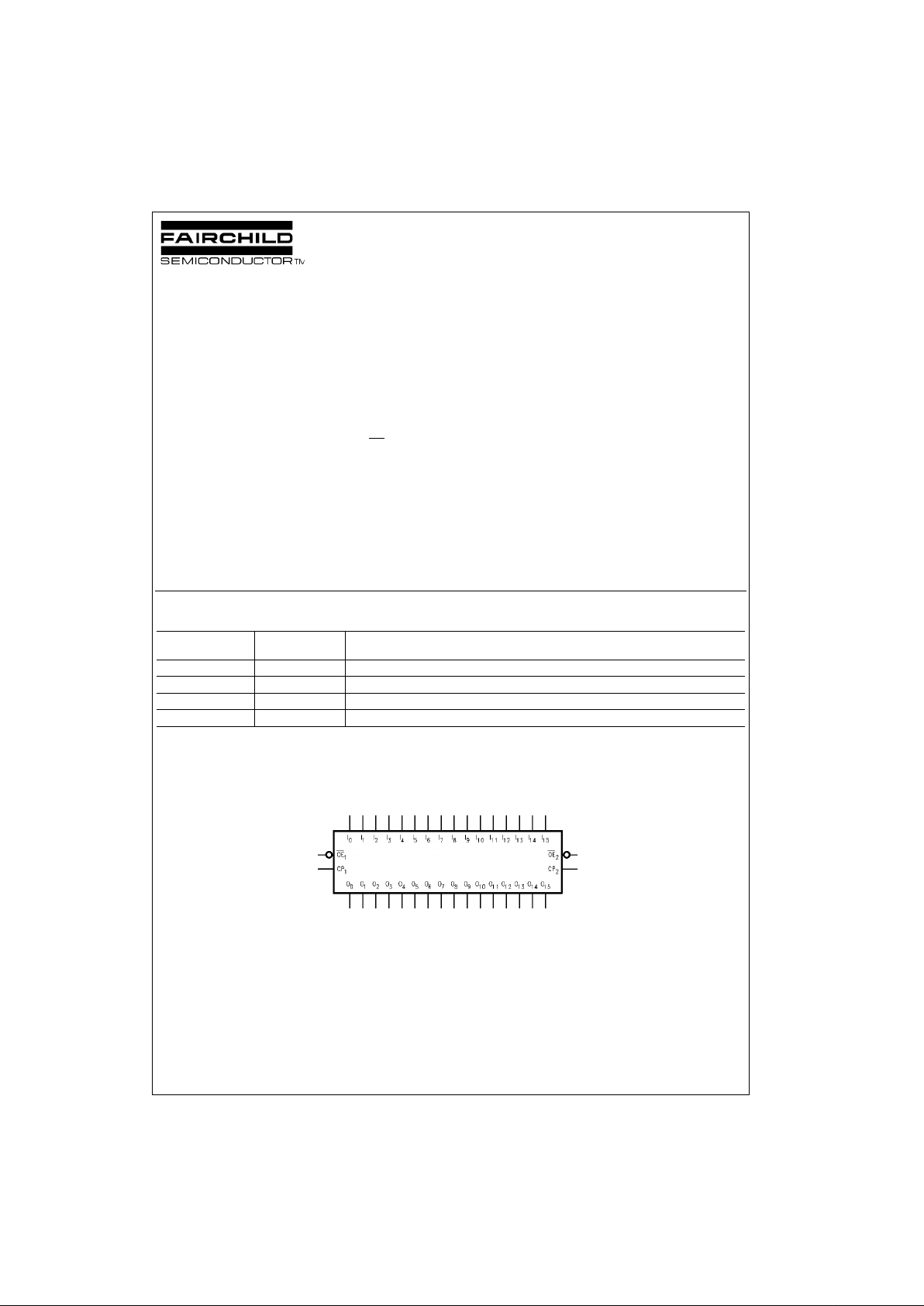
Logic Symbol
Order Number Package
Number
Package Descript ion
74LVT16374MEA MS48A 48-Lead Small Shrink Outline Package (SSOP), JEDEC MO-118, 0.300” Wide
74LVT16374MTD MTD48 48-Lead Thin Shrink Small Outline Package (TSSOP), JEDEC MO-153, 6.1mm Wide
74LVTH16374MEA MS48A 48-Lead Small Shrink Outline Package (SSOP), JEDEC MO-118, 0.300” Wide
74LVTH16374MTD MTD48 48-Lead Thin Shrink Small Outline Package (TSSOP), JEDEC MO-153, 6.1mm Wide
Page 2
www.fairchildsemi.com 2
74LVT16374 • 74LVTH16374
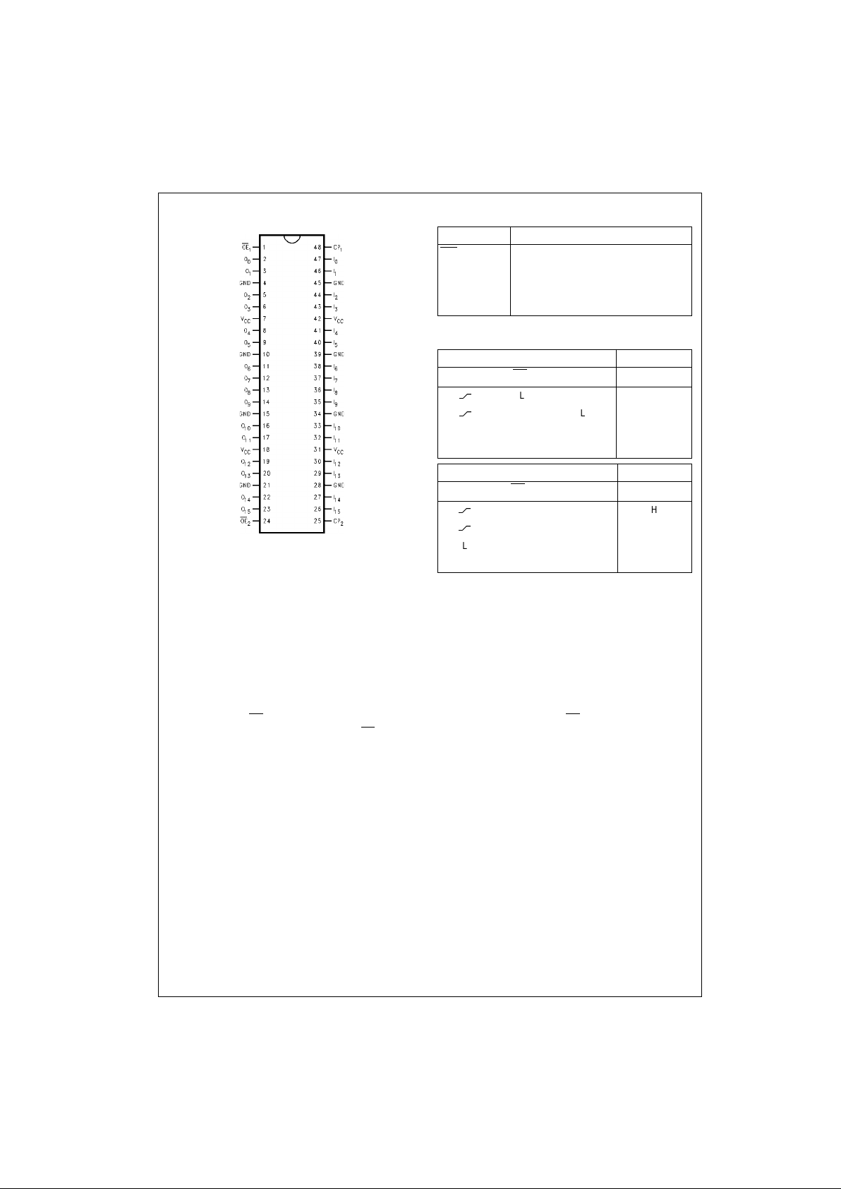
Connection Diagram Pin Descriptions
Tr uth Tables
H = HIGH Voltage Level
L = LOW Voltage Level
X = Immaterial
Z = HIGH Impedance
O
o
= Previous Oo before HIGH to LOW of CP
Functional Description
The LVT16374 and LVTH16374 consist of sixteen edge -trigge red flip- flop s with in dividual D-type inputs a nd 3-S TATE true
outputs. The device is byt e contro lled wi th eac h byte fun ctioni ng ident ically, but independe nt of the o ther. The control pins
can be shorted together to obtain full 16-bit operation. Each byte has a buffered clock and buffered Output Enable common
to all flip-flops wit hin that byte . T he description which follows app l ies to ea ch b yte. Each flip-flop will s tor e th e sta te of th eir
individual D-type input s that meet the setup an d hold time require ments o n the LOW-to- HIGH Cl ock (CP
n
) transition. With
the Output Enable (OE
n
) LOW, the contents of the flip-flops are available at the outputs. When OEn is HIGH, the outputs go
to the high impedance state. Operation of the OE
n
input does not affect the state of the flip-flops.
Pin Names Description
OE
n
Output Enable Input (Active LOW)
CP
n
Clock Pulse Input
I
0–I15
Inputs
O
0–O15
3-STATE Outputs
Inputs Outputs
CP
1
OE
1
I0–I
7
O0–O
7
LH H
LL L
LL X O
o
XH X Z
Inputs Outputs
CP
2
OE
2
I8–I
15
O8–O
15
LH H
LL L
LL X O
o
XH X Z
Page 3
3 www.fairchildsemi.com
74LVT16374 • 74LVTH16374
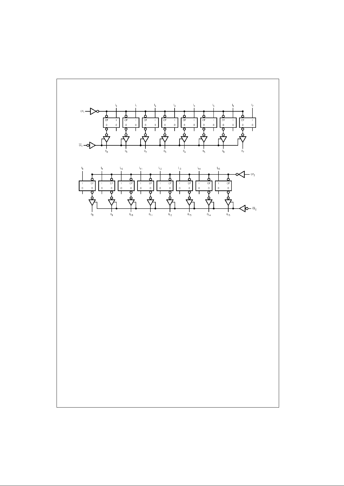
Logic Diagrams
Byte 1 (0:7)
Byte 2 (8:15)
Please note that thes e diagrams are provided f or t he understanding of logic operaiton and should not be used to estimate prop agation delays.
Page 4

www.fairchildsemi.com 4
74LVT16374 • 74LVTH16374
Absolute Maximum Ratings(Note 1)
Recommended Operating Conditions
Note 1: Absolute Maximum continuous ratings are those valu es beyond which da m age to the device may occur. Exposure to the s e c onditions or conditions
beyond those indic ated may adversely affect device reliability. Functional opera ti on under absolute maximum rated conditions is not implied.
Note 2: I
O
Absolute Maximum Rating must be observed.
DC Electrical Characteristics
Symbol Parameter Value Conditions Units
V
CC
Supply Voltage −0.5 to +4.6 V
V
I
DC Input Voltage −0.5 to +7.0 V
V
O
DC Output Voltage −0.5 to +7.0 Output in 3-STATE V
−0.5 to +7.0 Output in High or Low State (Note 2)
I
IK
DC Input Diode Current −50 VI < GND mA
I
OK
DC Output Diode Current −50 VO < GND mA
I
O
DC Output Current 64 VO > VCCOutput at High State
mA
128 V
O
> VCCOutput at Low State
I
CC
DC Supply Current per Supply Pin ±64 mA
I
GND
DC Ground Current per Ground Pin ±128 mA
T
STG
Storage Temperature −65 to +150 °C
Symbol Parameter Min Max Units
V
CC
Supply Voltage 2.7 3.6 V
V
I
Input Voltage 0 5.5 V
I
OH
High-Level Output Current −32 mA
I
OL
Low-Level Output Current 64 mA
T
A
Free-Air Operating Temperature −40 85 °C
∆t/∆V Input Edge Rate, V
IN
= 0.8V–2.0V, VCC = 3.0V 0 10 ns/V
Symbol Parameter
V
CC
(V)
T A = −40°C to +85°C
Units Conditions
Min Typ Max
(Note 3)
V
IK
Input Clamp Diode Voltage 2.7 −1.2 V II = −18 mA
V
IH
Input HIGH Voltage 2.7–3.6 2.0 V VO ≤ 0.1V or
VO ≥ VCC − 0.1V
V
IL
Input LOW Voltage 2.7–3.6 0.8 V
V
OH
Output HIGH Voltage 2.7–3.6 VCC − 0.2 V IOH = −100 µA
2.7 2.4 IOH = −8 mA
3.0 2.0 IOH = −32 mA
V
OL
Output LOW Voltage 2.7 0.2 V IOL = 100 µA
2.7 0.5 IOL = 24 mA
3.0 0.4 IOL = 16 mA
3.0 0.5 IOL = 32 mA
3.0 0.55 IOL = 64 mA
I
I(HOLD)
Bushold Input Minimum Drive 3.0 75 µAVI = 0.8V
(Note 4) −75 VI = 2.0V
I
I(OD)
Bushold Input Over-Drive
Current to Change State
3.0 500 µA(Note 5)
(Note 4) −500 (Note 6)
I
I
Input Current 3.6 10 µAVI = 5.5V
Control Pins 3.6 ±1V
I
= 0V or V
CC
Data Pins 3.6 −5V
I
= 0V
1V
I
= V
CC
I
OFF
Power Off Leakage Current 0 ±100 µA0V ≤ VI or VO ≤ 5.5V
I
PU/PD
Power up/down 3-STATE 0–1.5V ±100 µAVO = 0.5V to 3.0V
Output Current VI = GND or V
CC
I
OZL
3-STATE Output Leakage Current 3.6 −5 µAVO = 0.5V
I
OZH
3-STATE Output Leakage Current 3.6 5 µAVO = 3.0V
Page 5

5 www.fairchildsemi.com
74LVT16374 • 74LVTH16374
DC Electrical Characteristics (Continued)
Note 3: All typical value s are at VCC = 3.3V, TA = 25°C.
Note 4: Applies to bushold versions only (74LVTH1637 4).
Note 5: An external driver must source at least the specified current to switch from LOW to HIGH.
Note 6: An external driver must sink at least the specified current to switch from HIGH to LOW.
Note 7: This is the increas e in supply current for eac h input that is at the specif ied voltage level rather than V
CC
or GND.
Dynamic Switching Characteristics (Note 8)
Note 8: Characterize d in SSOP package. Guaranteed paramete r, but not tes te d.
Note 9: Max number of outputs defined as (n). n−1 data inputs are driven 0V to 3V. Output under test held LOW.
AC Electrical Characteristics
Note 10: All typical valu es are at VCC = 3.3V, TA = 25°C.
Note 11: Skew is defined as the absolute value of the difference between the actual propagation delay for any two separate outputs of the same device. The
specification applies t o any outputs switching in th e s am e direction, either HIGH to LOW (t
OSHL
) or LOW to HIGH (t
OSLH
).
Capacitance (Note 12)
Note 12: Capacitanc e is m easured at frequency f = 1 MHz, per MIL-STD-883, Method 3012.
Symbol Parameter
V
CC
(V)
T A = −40°C to +85°C
Units Conditions
Min Typ Max
(Note 3)
I
OZH
+ 3-STATE Output Leakage Current 3.6 10 µAVCC < VO ≤ 5.5V
I
CCH
Power Supply Current 3.6 0.19 mA Outputs High
I
CCL
Power Supply Current 3.6 5 mA Outputs Low
I
CCZ
Power Supply Current 3.6 0.19 mA Outputs Disabled
I
CCZ
+ Power Supply Current 3.6 0.19 mA VCC ≤ VO ≤ 5.5V,
Outputs Disabled
∆I
CC
Increase in Power Supply Current 3.6 0.2 mA One Input at VCC − 0.6V
(Note 7) Other Inputs at VCC or GND
Symbol Parameter
V
CC
(V)
TA = 25°C
Units
Conditions
CL = 50 pF ,
RL = 500Ω
Min Typ Max
V
OLP
Quiet Output Maximum Dynamic V
OL
3.3 0.8 V (Note 9)
V
OLV
Quiet Output Minimum Dynamic V
OL
3.3 −0.8 V (Note 9)
Symbol Parameter
TA = −40°C to +85°C
CL = 50 pF, RL = 500Ω
Units
VCC = 3.3V ±0.3V VCC = 2.7V
Min
Typ
(Note 10)
Max Min Max
f
max
Maximum Clock Frequency 160 160 MHz
t
PHL
Propagation Delay 1.9 4.3 1.9 4.6
ns
t
PLH
CP to O
n
1.6 4.5 1.6 5.2
t
PZL
Output Enable Time 1.3 4.4 1.3 5.0
ns
t
PZH
1.0 4.5 1.0 5.4
t
PLZ
Output Disable Time 1.5 4.6 1.5 4.8
ns
t
PHZ
2.0 5.0 2.0 5.4
t
S
Setup Time 1.8 2.0 ns
t
H
Hold Time 0.8 0.1 ns
t
W
Pulse Width 3.0 3.0 ns
t
OSHL
Output to Output Skew (Note 11) 1.0 1.0
ns
t
OSLH
1.0 1.0
Symbol Parameter Conditions Typical Units
C
IN
Input Capacitance VCC = Open, VI = 0V or V
CC
4pF
C
OUT
Output Capacitance VCC = 3.0V, VO = 0V or V
CC
8pF
Page 6

www.fairchildsemi.com 6
74LVT16374 • 74LVTH16374
Physical Dimensions inches (millimeters) unless otherwise noted
48-Lead Small Shrink Outline Package (SSOP), JEDEC MO-118, 0.300” Wide
Package Number MS48A
48-Lead Thin Shrink Small Outline Package (TSSOP), JEDEC MO-153, 6.1mm Wide
Package Number MTD48
Page 7

Fairchild does not assume any responsibility for use of any circuitry described, no circuit patent licenses are implied and Fairchild reserves the right at any time without notice to change said circuitry and specifications.
74LVT16374 • 74LVTH16374 Low Voltage 16-Bit D-Type Flip-Flop with 3-STATE Outputs
LIFE SUPPORT POLICY
FAIRCHILD’S PRODUCTS ARE NOT AUTHORIZED FOR USE AS CRITICAL COMPONENTS IN LIFE SUPPORT
DEVICES OR SYSTEMS WITHOUT THE EXPRESS WRITTEN APPROVAL OF THE PRESIDENT OF FAIRCHILD
SEMICONDUCTOR CORPORATION. As used herein:
1. Life support devices or system s are de vices o r syste ms
which, (a) are intended for surgical implant into the
body, or (b) support or sustain life, and (c) whose failure
to perform when properly used in accordance with
instructions for use provide d in the lab el ing , can be re asonably expected to result in a significant in jury to the
user.
2. A critical component in any component of a life support
device or system whose failure to perform can be r easonably expected to cau se th e f ail ur e o f the life sup por t
device or system, or to affect its safety or effectiveness.
www.fairchildsemi.com
 Loading...