

Datasheet 74LVTH16245MTDX, 74LVTH16245MTD, 74LVTH16245MEAX, 74LVTH16245MEA, 74LVT16245MTDX Datasheet (Fairchild Semiconductor)
...Page 1
January 1999
Revised November 1999
74LVT16245 • 74LVTH16245
Low Voltage 16-Bit Transceiver with 3- STATE Outputs
74LVT16245 • 74LVTH16245 Low Voltage 16-Bit Tr ansceiver with 3-STA TE Outputs
General Description
The LVT16245 and LVTH16245 contain sixteen non-inverting bidirectional buffers with 3-STATE outputs and is
intended for bus orien ted applications. The de vice is byte
controlled. Each byte has separate control inputs which
can be shorted toget her for full 16-bit ope ration. The T/R
inputs determine the direction of data flow through the
device. The OE
placing them in a high impedance state.
The LVTH16245 data inputs includ e bushold, eliminating
the need for external pull-up resistors to hold unused
inputs.
These non-inverting transceivers are designed for low-voltage (3.3V) V
vide a TTL interface to a 5V environment. Th e LVT16245
and LVTH16245 are fabricated with an adva nced B iCMOS
technology to achieve high speed ope ration similar to 5V
ABT while maintaining low power dissipation.
inputs disable bo th the A and B ports by
applications, but with the capability to pro-
CC
Features
■ Input and output interface capability to systems at
5V V
CC
■ Bushold data inputs elimi nate th e need fo r extern al pullup resistors to hold unused inputs (74LVTH16245), also
available without bushold feat ure (74LVT16245).
■ Live insertion/extraction per mi tt ed
■ Power Up/Down high impedance provides glitch-free
bus loading
■ Outputs source/sink −32 mA/+64 mA
■ Functionally compatible with the 74 series 16245
■ Latch-up performance exce eds 500 mA
Ordering Code:
Order Number
74LVT16245MEA MS48A 48-Lead Small Shrink Outline Package (SSOP), JEDEC MO-118, 0.300” Wide
74LVT16245MTD MTD48 48-Lead Thin Shrink Small Outline Package (TSSOP), JEDEC MO-153, 6.1mm Wide
74LVTH16245MEA MS48A 48-Lead Small Shrink Outline Package (SSOP), JEDEC MO-118, 0.300” Wide
74LVTH16245MTD MTD48 48-Lead Thin Shrink Small Outline Package (TSSOP), JEDEC MO-153, 6.1mm Wide
Devices also availab l e in Tape and Reel. Specify by appending su ffix let te r “X” to the ordering code.
Package
Number
Package Descript ion
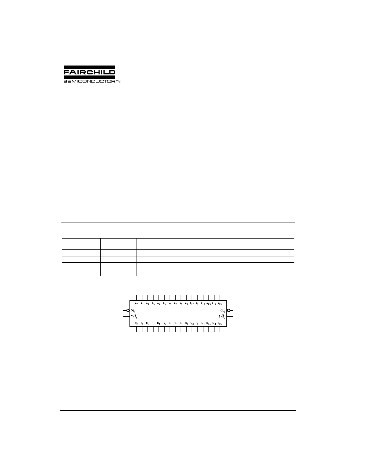
Logic Symbol
© 1999 Fairchild Semiconductor Corporation DS500152 www.fairchildsemi.com
Page 2
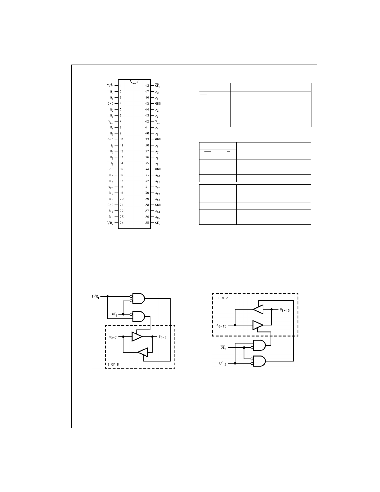
Connection Diagram Pin Descriptions
Pin Names Description
OE
T/R
A
0–A15
B
0–B15
n
n
Output Enable Input (Active LOW)
Transmit/Receive Input
Side A Inputs/3-STATE Outputs
Side B Inputs/3-STATE Outputs
Truth Tables
74LVT16245 • 74LVTH16245
Inputs
OE
T/R
1
1
L L Bus B0–B7 Data to Bus A0–A
L H Bus A0–A7 Data to Bus B0–B
H X HIGH–Z State on A0–A7,B0–B
Inputs
OE
T/R
2
2
L L Bus B8–B15 Data to Bus A8–A
L H Bus A8–A15 Data to Bus B8–B
HXHIGH–Z State on A8–A15,B8–B
H = HIGH Voltage Level
L = LOW Voltage Level
X = Immaterial
Z = High Impedance
Outputs
Outputs
Functional Description
The LVT16245 and LVTH16245 contain sixteen non-inverting bidirectional buffers with 3-STA T E outputs. The device is byte
controlled with eac h byte functioning identically, but independent of the other. The control pins can be sho rted together to
obtain full 16-bit operation.
7
7
7
15
15
15
Logic Diagrams
Note: Please note that these diagrams are provided only for the understanding of logic operations and should not be used to estimat e propagation delays.
www.fairchildsemi.com 2
Page 3

Absolute Maximum Ratings(Note 1)
Symbol Parameter Value Conditions Units
V
CC
V
I
V
O
Supply Voltage −0.5 to +4.6 V
DC Input Voltage −0.5 to +7.0 V
Output Voltage −0.5 to +7.0 Output in 3-STATE
−0.5 to +7.0 Output in HIGH or LOW State (Note 2)
I
I
I
I
I
T
IK
OK
O
CC
GND
STG
DC Input Diode Current −50 VI < GND mA
DC Output Diode Current −50 VO < GND mA
DC Output Current 64 Output at HIGH State, VO > V
128 Output at LOW St ate, V
O
> V
CC
CC
mA
DC Supply Current per Supply Pin ±64 mA
DC Ground Current per Ground Pin ±128 mA
Storage Temperature Range −65 to +150 °C
Recommended Operating Conditions
Symbol Parameter Min Max Units
V
CC
V
I
I
OH
I
OL
T
A
∆t/∆V Input Edge Rate, V
Note 1: Absolute Maximum continuous ratings are those values beyond which damage to the device may occur. Exposure to these conditions or conditions
beyond those indica te d m ay adversely affect de v ic e reliability. Functional operation under absolute maxi m um rated conditions is not implied.
Absolute Maximum Ratings must be observed.
Note 2: I
O
Supply Voltage 2.7 3.6 V
Input Voltage 0 5.5 V
HIGH-Level Output Current −32 mA
LOW-Level Output Current 64 mA
Free-Air Operating Temperature −40 +85 °C
= 0.8V–2.0V, VCC = 3.0V 0 10 ns/V
IN
74LVT16245 • 74LVTH16245
V
DC Electrical Characteristics
V
Symbol Parameter
V
IK
V
IH
V
IL
V
OH
V
OL
I
I(HOLD)
(Note 3) −75 VI = 2.0V
I
I(OD)
(Note 3) Current to Change State −500 (Note 5)
I
I
I
OFF
I
PU/PD
I
OZL
I
OZL
I
OZH
Input Clamp Diode Voltage 2.7 −1.2 V II = −18 mA
Input HIGH Voltage 2.7–3.6 2.0 V VO ≤ 0.1V or
Input LOW Voltage 2.7–3.6 0.8 V VO ≥ V
Output HIGH Voltage 2.7–3.6 V
Output LOW Voltage 2.7 0.2
Bushold Input Minimum Drive 3.0 75
Bushold Input Over-Drive 3.0 500
Input Current 3.6 10
Control Pins 3.6 ±1V
Data Pins 3.6 −5V
Power Off Leakage Current 0 ±100 µA0V ≤ VI or VO ≤ 5.5V
Power Up/Down 3-STATE 0–1.5 ±100 µAVO = 0.5V to 3.0V
Output Current VI = GND or V
3-STATE Output Leakage Current 3.6 −5 µAVO = 0.5V
(Note 3) 3-STATE Output Leakage Current 3.6 −5 µAVO = 0.0V
3-STATE Output Leakage Current 3.6 5 µAVO = 3.0V
CC
(V) Min Max
2.7 2.4 I
3.0 2.0 IOH = −32 mA
2.7 0.5 I
3.0 0.4 IOL = 16 mA
3.0 0.5 IOL = 32 mA
3.0 0.55 IOL = 64 mA
TA = −40°C to +85°C
− 0.2
CC
1V
Units Conditions
IOH = −100 µA
V
V
µA
µA
µA
= −8 mA
OH
IOL = 100 µA
= 24 mA
OL
VI = 0.8V
(Note 4)
VI = 5.5V
= 0V or V
I
= 0V
I
= V
I
CC
CC
− 0.1V
CC
CC
3 www.fairchildsemi.com
Page 4

DC Electrical Characteristics (Continued)
V
Symbol Parameter
I
(Note 3) 3-STATE Output Leakage Current 3.6 5 µAVO = 3.6V
OZH
+ 3-STATE Output Leakage Current 3.6 10 µAVCC < VO ≤ 5.5V
I
OZH
I
I
I
I
CCH
CCL
CCZ
CCZ
Power Supply Current 3.6 0.19 mA Outputs HIGH
Power Supply Current 3.6 5.0 mA Outputs LOW
Power Supply Current 3.6 0.19 mA Outputs Disabled
+ Power Supply Current 3.6 0.19 mA VCC ≤ VO ≤ 5.5V,
CC
(V) Min Max
TA = −40°C to +85°C
Units Conditions
Outputs Disabled
∆I
CC
74LVT16245 • 74LVTH16245
Note 3: Applies to bushold versions only (74LVTH16245).
Note 4: An external driver must source at least the specified current to switch from LOW-to-HIGH.
Note 5: An external driver must s ink at least the specified current to switch from HI GH-to-LOW.
Note 6: This is the increase in supply current for each input that is at the specif ied voltage level rather t han V
Increase in Power Supply Current 3.6 0.2 mA One Input at VCC − 0.6V
(Note 6) Other Inputs at V
or GND.
CC
Dynamic Switching Characteristics (Note 7)
V
Symbol Parameter
V
OLP
V
OLV
Note 7: Characterized in SSO P package. Guarant eed parameter, but not teste d.
Note 8: Max number of output s d ef i ned as (n). n−1 data inputs are driven 0V to 3V. Output under test held LOW.
Quiet Output Maximum Dynamic V
Quiet Output Minimum Dynamic V
OL
OL
CC
(V)
3.3 0.8 V (Note 8)
3.3 −0.8 V (Note 8)
TA = 25°C
Min Typ Max
Units
Conditions
CL = 50 pF, RL = 500Ω
AC Electrical Characteristics
TA = −40°C to +85°C
Symbol Parameter
VCC = 3.3V ± 0.3V VCC = 2.7V
Min Max Min Max
t
PLH
t
PHL
t
PZH
t
PZL
t
PHZ
t
PLZ
t
OSHL
t
OSLH
Note 9: Skew is defined as the absolute value of the difference between the actual propagation delay for any two separate outputs of the same device. The
specification applies to any outputs switc hing in the same direction, eit her HIGH-to-LOW (t
Propagation Delay Data to Output 1.5 3.5 1.5 3.9
1.3 3.5 1.3 3.9
Output Enable Time 1.5 4.5 1.5 5.3
1.6 5.3 1.6 6.9
Output Disable Time 2.3 5.4 2.3 6.1
2.2 5.1 2.2 5.4
Output to Output Skew
(Note 9)
CL = 50 pF, RL = 500Ω
1.0 1.0 ns
) or LOW-to-HIGH (t
OSHL
). Parameter guaranteed by design.
OSLH
CC
Units
or GND
ns
ns
ns
Capacitance (Note 10)
Symbol Parameter Conditions Typical Units
C
IN
C
I/O
Note 10: Capacitance is mea s ured at frequency f = 1 MHz , per MIL-STD-883, M et hod 3012.
www.fairchildsemi.com 4
Input Capacitance VCC = 0V, VI = 0V or V
Input/Output Capacitance VCC = 3.0V, VO = 0V or V
CC
CC
4pF
8pF
Page 5

Physical Dimensions inches (millimeters) unless otherwise noted
74LVT16245 • 74LVTH16245
48-Lead Small Shrink Outline Package (SSOP), JEDEC MO-118, 0.300” Wide
Package Number MS48A
5 www.fairchildsemi.com
Page 6

Physical Dimensions inches (millimeters) unless otherwise noted (Continued)
74LVT16245 • 74LVTH16245 Low Voltage 16-Bit Transceiver with 3-STATE Outputs
48-Lead Thin Shrink Small Outline Package (TSSOP), JEDEC MO-153, 6.1mm Wide
Fairchild does not assume any responsibility for use of any circuitr y described, no circuit patent licenses are implied a nd
Fairchild reserves the right at any time without notice to change said circuitry and specifications.
LIFE SUPPORT POLICY
FAIRCHILD’S PRODUCTS ARE NOT AUTHORIZED FOR USE AS CRITICAL COMPONENTS IN LIFE SUPPORT
DEVICES OR SYSTEMS WITHOUT THE EXPRESS WRITTEN APPROVAL OF THE PRESIDENT OF FAIRCHILD
SEMICONDUCTOR CORPORATION. As used herein:
1. Life support devices or systems are devices or systems
which, (a) are intended for surgical implant into the
body, or (b) support or sustain life, and (c) whose failure
to perform when properly used in accordance with
instructions for use provided in the labeling, can be reasonably expected to result in a significant inju ry to the
user.
www.fairchildsemi.com 6
Package Number MTD48
2. A critical component in any com ponen t of a life su pport
device or system whose failu re to perform can be reasonably expected to cause the failure of the li fe su pp ort
device or system, or to affect its safety or effectiveness.
www.fairchildsemi.com
 Loading...