

Page 1

74LVT20
3.3V Dual 4-input NAND gate
Product specification 1996 Aug 28
INTEGRATED CIRCUITS
IC24 Data Handbook
Page 2

Philips Semiconductors Product specification
74LVT203.3V Dual 4-input NAND gate
2
1996 Aug 28 853-1871 17244
QUICK REFERENCE DATA
SYMBOL PARAMETER
CONDITIONS
T
amb
= 25°C;
GND = 0V
TYPICAL UNIT
t
PLH
t
PHL
Propagation
delay
An, Bn, Cn, Dn
to Y
n
CL = 50pF;
V
CC
= 3.3V
3.4
3.2
ns
C
IN
Input
capacitance
VI = 0V or 3.0V 3 pF
I
CCL
Total supply
current
Outputs Low;
V
CC
= 3.6V
0.5 mA
PIN CONFIGURATION
14
13
12
11
10
9
87
6
5
4
3
2
1
GND
V
CC
B1
A1
Y1
NC
D1
C1
A0
B0
Y
0
NC
C0
D0
SA00350
PIN DESCRIPTION
PIN
NUMBER
SYMBOL NAME AND FUNCTION
1, 2, 4, 5, 9,
10, 12, 13
An, Bn,
Cn, Dn
Data inputs
6, 8 Yn Data outputs
7 GND Ground (0V)
14 V
CC
Positive supply voltage
LOGIC SYMBOL
D0 A1 B1A0 B0 C0 C1 D1
Y0 Y1
6 8
1 2 4 5 9 10 12 13
VCC = Pin 14
GND = Pin 7
SA00351
LOGIC DIAGRAM
VCC = Pin 14
GND = Pin 7
SA00352
Y0
6
1
2
4
A0
B0
C0
5
D0
Y1
8
9
10
12
A1
B1
C1
13
D1
SF00068
&
6
8
1
2
4
5
9
10
12
13
FUNCTION TABLE
INPUTS OUTPUT
Dna Dnb Dnc Dnd Qn
L X X X H
X L X X H
X X L X H
X X X L H
H H H H L
NOTES:
H = High voltage level
L = Low voltage level
X = Don’t care
ORDERING INFORMATION
PACKAGES TEMPERATURE RANGE OUTSIDE NORTH AMERICA NORTH AMERICA DWG NUMBER
14-Pin Plastic SO –40°C to +85°C 74LVT20 D 74LVT20 D SOT108-1
14-Pin Plastic SSOP –40°C to +85°C 74LVT20 DB 74LVT20 DB SOT337-1
14-Pin PlasticTSSOP –40°C to +85°C 74LVT20 PW 74LVT20PW DH SOT402-1
LOGIC SYMBOL (IEEE/IEC)
Page 3

Philips Semiconductors Product specification
74LVT203.3V Dual 4-input NAND gate
1996 Aug 28
3
ABSOLUTE MAXIMUM RATINGS
1, 2
SYMBOL
PARAMETER CONDITIONS RATING UNIT
V
CC
DC supply voltage –0.5 to +4.6 V
I
IK
DC input diode current VI < 0 –50 mA
V
I
DC input voltage
3
–0.5 to +7.0 V
I
OK
DC output diode current VO < 0 –50 mA
V
OUT
DC output voltage
3
Output in Off or High state –0.5 to +7.0 V
Output in High state –32
I
OUT
DC output current
Output in Low state 64
mA
T
stg
Storage temperature range –65 to 150 °C
NOTES:
1. Stresses beyond those listed may cause permanent damage to the device. These are stress ratings only and functional operation of the
device at these or any other conditions beyond those indicated under “recommended operating conditions” is not implied. Exposure to
absolute-maximum-rated conditions for extended periods may affect device reliability.
2. The performance capability of a high-performance integrated circuit in conjunction with its thermal environment can create junction
temperatures which are detrimental to reliability. The maximum junction temperature of this integrated circuit should not exceed 150°C.
3. The input and output negative voltage ratings may be exceeded if the input and output clamp current ratings are observed.
RECOMMENDED OPERATING CONDITIONS
LIMITS
SYMBOL
PARAMETER
MIN MAX
UNIT
V
CC
DC supply voltage 2.7 3.6 V
V
I
Input voltage 0 5.5 V
V
IH
High-level input voltage 2.0 V
V
IL
Low-level Input voltage 0.8 V
I
OH
High-level output current –20 mA
Low-level output current 32
I
OL
Low-level output current; current duty cycle ≤ 50%, f ≥ 1kHz 48
mA
T
amb
Operating free-air temperature range –40 +85 °C
Page 4
Philips Semiconductors Product specification
74LVT203.3V Dual 4-input NAND gate
1996 Aug 28
4
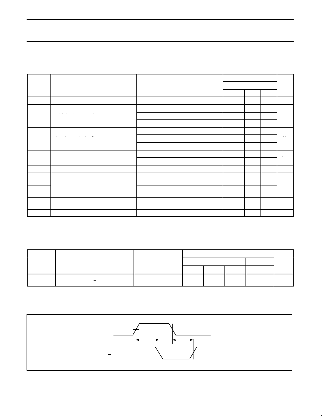
DC ELECTRICAL CHARACTERISTICS
Over recommended operating conditions
Voltages are referenced to GND (ground = 0V)
LIMITS
SYMBOL
PARAMETER
TEST CONDITIONS Temp = -40°C to +85°C UNIT
MIN TYP1MAX
V
IK
Input clamp voltage VCC = 2.7V; IIK = –18mA –1.2 V
VCC = 2.7 to 3.6V; IOH = –100µA VCC–0.2
VCC = 2.7V; IOH = –6mA 2.4
VCC = 3.0V; IOH = –20mA 2.0
VCC = 2.7V; IOL = 100µA 0.2
VCC = 2.7V; IOL = 24mA 0.5
VCC = 3.0V; IOL = 32mA 0.5
VCC = 0 or 3.6V; VI = 5.5V 10
IIInput leakage current
VCC = 3.6V; VI = VCC or GND ±1
µA
I
OFF
Output off current VCC = 0V; VI or VO = 0 to 4.5V ±100 µA
I
CCH
VCC = 3.6V; Outputs High, VI = GND or
V
CC,
I
O =
0
0.02
I
CCL
Quiescent supply current
VCC = 3.6V; Outputs Low, VI = GND or V
CC,
I
O =
0
0.5 1.2
mA
∆I
CC
Additional supply current per input pin
2
VCC = 3V to 3.6V; One input at VCC–0.6V,
Other inputs at V
CC
or GND
0.2 µA
C
I
Input capacitance VI = 3V or 0 3 pF
NOTES:
1. All typical values are at V
CC
= 3.3V and T
amb
= 25°C.
2. This is the increase in supply current for each input at the specificed voltage level other than VCC or GND.
AC CHARACTERISTICS
GND = 0V; tR = tF = 2.5ns; CL = 50pF, RL = 500Ω; T
amb
= –40°C to +85°C.
LIMITS
SYMBOL PARAMETER WAVEFORM VCC = 3.3V ± 0.3V VCC = 2.7V UNIT
MIN TYP
1
MAX MAX
t
PLH
t
PHL
Propagation delay
An, Bn, Cn, Dn to Yn
1
1.0
1.0
3.4
3.2
5.4
4.4
6.4
4.3
ns
NOTE:
1. All typical values are at V
CC
= 3.3V and T
amb
= 25°C.
AC WAVEFORMS
VM = 1.5V, VIN = GND to 2.7V
V
M
V
M
V
M
V
M
Qn
Dna, Dnb, Dnc, Dnd
t
PHL
t
PLH
SF00069
Waveform 1. Propagation Delay for Inverting Outputs
V
OH
High-level output voltage
V
OL
Low-level output voltage
V
V
Page 5
Philips Semiconductors Product specification
74LVT203.3V Dual 4-input NAND gate
1996 Aug 28
5
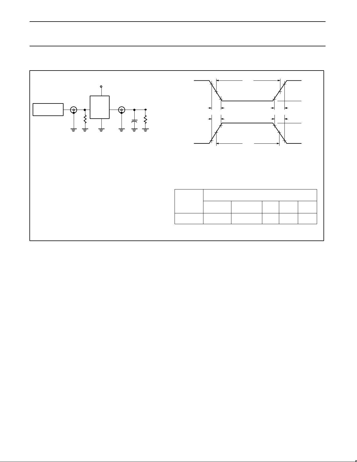
TEST CIRCUIT AND WAVEFORMS
V
M
V
M
t
W
AMP (V)
NEGATIVE
PULSE
10% 10%
90%
90%
0V
V
M
V
M
t
W
AMP (V)
POSITIVE
PULSE
90% 90%
10%
10%
0V
t
THL
(tF)
t
TLH
(tR) t
THL
(tF)
t
TLH
(tR)
VM = 1.5V
Input Pulse Definition
DEFINITIONS
RL = Load resistor; see AC CHARACTERISTICS for value.
CL = Load capacitance includes jig and probe capacitance;
see AC CHARACTERISTICS for value.
RT = Termination resistance should be equal to Z
OUT
of
pulse generators.
INPUT PULSE REQUIREMENTS
FAMILY
Amplitude Rep. Rate t
W
t
R
t
F
74LVT 2.7V ≤10MHz 500ns ≤2.5ns ≤2.5ns
PULSE
GENERATOR
V
IN
D.U.T.
V
OUT
C
L
V
CC
Test Circuit for Outputs
R
T
R
L
SV00022
Page 6
Philips Semiconductors Product specification
74LVT203.3V Dual 4-input NAND gate
1996 Aug 28
6
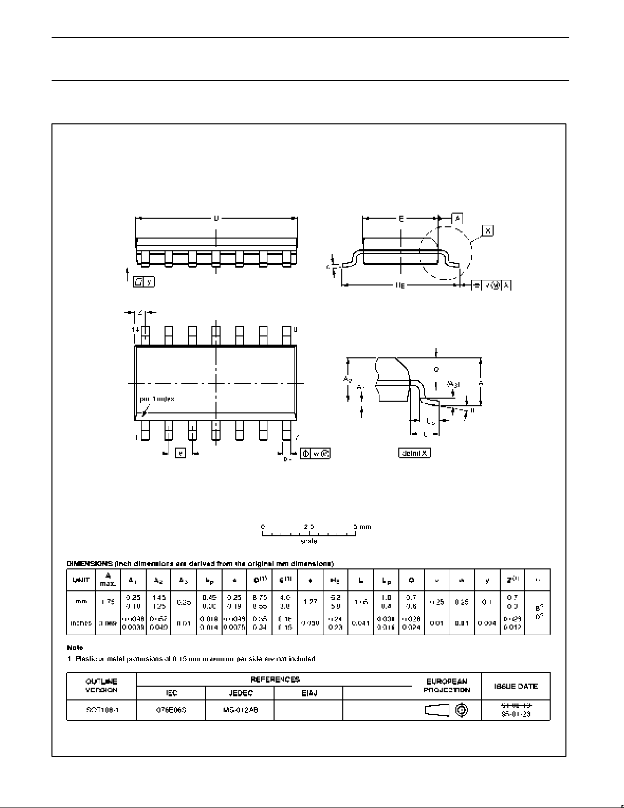
SO14: plastic small outline package; 14 leads; body width 3.9 mm SOT108-1
Page 7
Philips Semiconductors Product specification
74LVT203.3V Dual 4-input NAND gate
1996 Aug 28
7
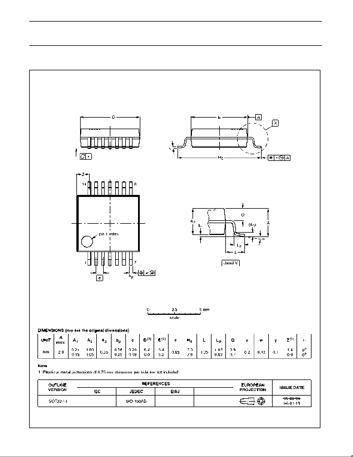
SSOP14: plastic shrink small outline package; 14 leads; body width 5.3 mm SOT337-1
Page 8
Philips Semiconductors Product specification
74LVT203.3V Dual 4-input NAND gate
1996 Aug 28
8
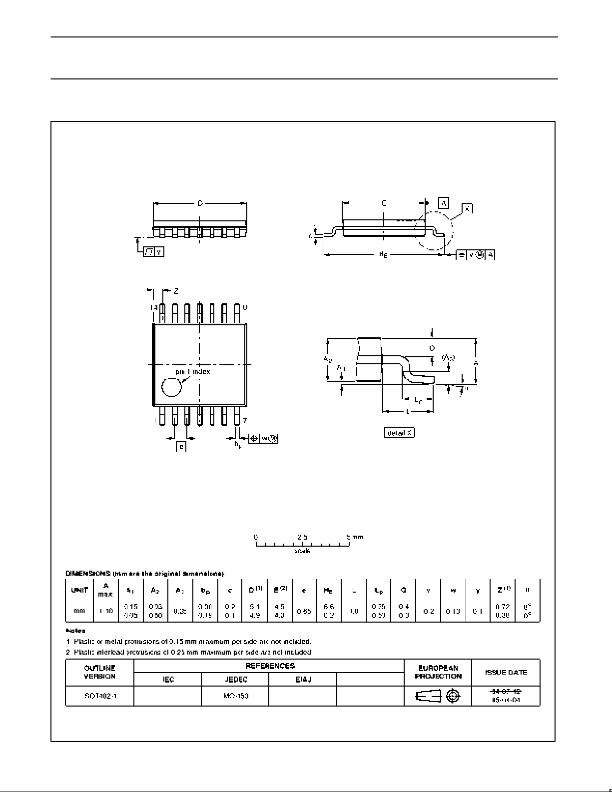
TSSOP14: plastic thin shrink small outline package; 14 leads; body width 4.4 mm SOT402-1
Page 9

Philips Semiconductors Product specification
74LVT203.3V Dual 4-input NAND gate
1996 Aug 28
9
NOTES
Page 10

Philips Semiconductors Product specification
74LVT203.3V Dual 4-input NAND gate
Philips Semiconductors and Philips Electronics North America Corporation reserve the right to make changes, without notice, in the products,
including circuits, standard cells, and/or software, described or contained herein in order to improve design and/or performance. Philips
Semiconductors assumes no responsibility or liability for the use of any of these products, conveys no license or title under any patent, copyright,
or mask work right to these products, and makes no representations or warranties that these products are free from patent, copyright, or mask
work right infringement, unless otherwise specified. Applications that are described herein for any of these products are for illustrative purposes
only. Philips Semiconductors makes no representation or warranty that such applications will be suitable for the specified use without further testing
or modification.
LIFE SUPPORT APPLICATIONS
Philips Semiconductors and Philips Electronics North America Corporation Products are not designed for use in life support appliances, devices,
or systems where malfunction of a Philips Semiconductors and Philips Electronics North America Corporation Product can reasonably be expected
to result in a personal injury. Philips Semiconductors and Philips Electronics North America Corporation customers using or selling Philips
Semiconductors and Philips Electronics North America Corporation Products for use in such applications do so at their own risk and agree to fully
indemnify Philips Semiconductors and Philips Electronics North America Corporation for any damages resulting from such improper use or sale.
This data sheet contains preliminary data, and supplementary data will be published at a later date. Philips
Semiconductors reserves the right to make changes at any time without notice in order to improve design
and supply the best possible product.
Philips Semiconductors
811 East Arques Avenue
P.O. Box 3409
Sunnyvale, California 94088–3409
Telephone 800-234-7381
DEFINITIONS
Data Sheet Identification Product Status Definition
Objective Specification
Preliminary Specification
Product Specification
Formative or in Design
Preproduction Product
Full Production
This data sheet contains the design target or goal specifications for product development. Specifications
may change in any manner without notice.
This data sheet contains Final Specifications. Philips Semiconductors reserves the right to make changes
at any time without notice, in order to improve design and supply the best possible product.
Philips Semiconductors and Philips Electronics North America Corporation
register eligible circuits under the Semiconductor Chip Protection Act.
Copyright Philips Electronics North America Corporation 1996
All rights reserved. Printed in U.S.A.
 Loading...