

Page 1
74LVQ04
Low Voltage Hex Inverter
General Description
The LVQ04 contains six inverters.
Features
n Ideal for low power/low noise 3.3V applications
n Guaranteed simultaneous switching noise level and
dynamic threshold performance
n Guaranteed pin-to-pin skew AC performance
n Guaranteed incident wave switching into 75Ω
Ordering Code:
Ordering Number Package Number Package Description
74LVQ04SC M14A 14-Lead (0.150" Wide) Molded Small Outline Package, SOIC JEDEC
74LVQ04SJ M14D 14-Lead Molded Small Outline Package, SOIC EIAJ
Devices also available in Tape and Reel. Specify by appending the suffix letter “X” to the ordering code.
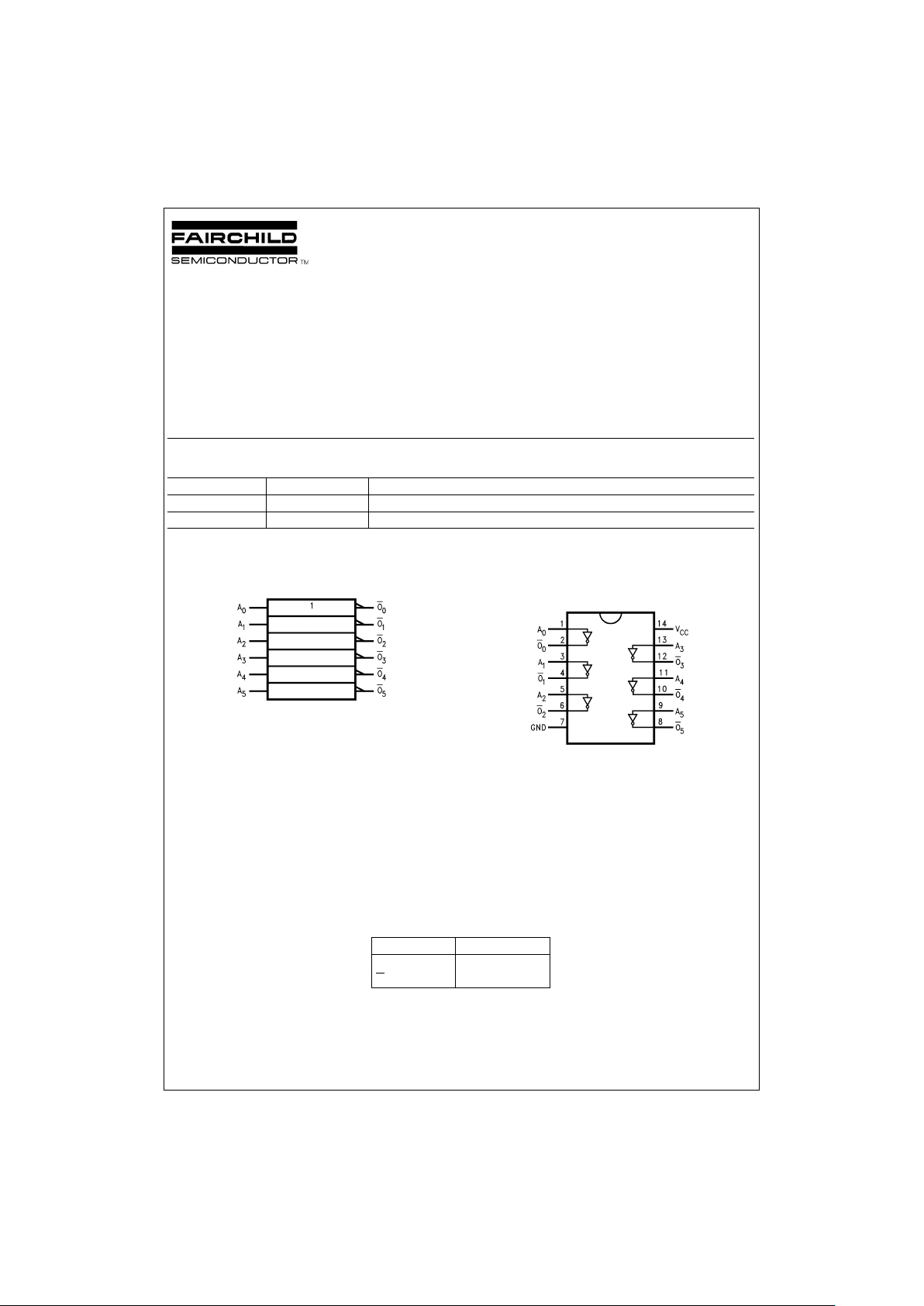
Logic Symbol Connection Diagram
Pin Descriptions
Pin Names Description
A
n
Inputs
O
n
Outputs
IEEE/IEC
DS011343-1
Pin Assignment
for SOIC JEDEC and EIAJ
DS011343-2
April 1998
74LVQ04 Low Voltage Hex Inverter
© 1998 Fairchild Semiconductor Corporation DS011343 www.fairchildsemi.com
Page 2
Absolute Maximum Ratings (Note 1)
Supply Voltage (V
CC
) −0.5V to +7.0V
DC Input Diode Current (I
IK
)
V
I
=
−0.5V −20 mA
V
I
=
V
CC
+ 0.5V +20 mA
DC Input Voltage (V
I
) −0.5V to VCC+ 0.5V
DC Output Diode Current (I
OK
)
V
O
=
−0.5V −20 mA
V
O
=
V
CC
+ 0.5V +20 mA
DC Output Voltage (V
O
) −0.5V to VCC+ 0.5V
DC Output Source
or Sink Current (I
O
)
±
50 mA
DC V
CC
or Ground Current
(I
CC
or I
GND
)
±
200 mA
Storage Temperature (T
STG
) −65˚C to +150˚C
DC Latch-Up Source or
Sink Current
±
100 mA
Recommended Operating
Conditions
(Note 2)
Supply Voltage (V
CC
) 2.0V to 3.6V
Input Voltage (V
I
) 0VtoV
CC
Output Voltage (VO) 0VtoV
CC
Operating Temperature (TA) −40˚C to +85˚C
Minimum Input Edge Rate (∆V/∆t)
V
IN
from 0.8V to 2.0V
V
CC
@
3.0V 125 mV/ns
Note 1: The “Absolute Maximum Ratings” are those values beyond which
the safety of the device cannot be guaranteed.The device should not be operated at these limits. The parametric values defined in the Electrical Characteristics tables are not guaranteed at the absolute maximum ratings. The
“Recommended Operating Conditions” table will define the conditions for actual device operation.
Note 2: Unused inputs must be held HIGH or LOW. They may not float.
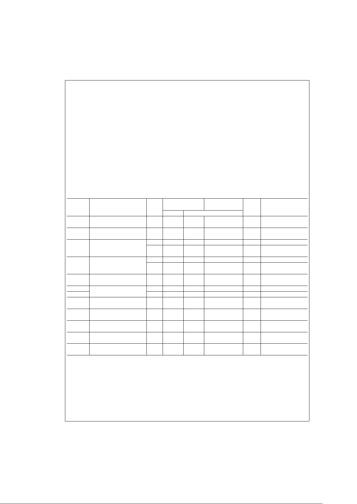
DC Electrical Characteristics
Symbol Parameter
V
CC
(V)
Units ConditionsT
A
=
+25˚C T
A
=
−40˚C to +85˚C
Typ Guaranteed Limits
V
IH
Minimum High Level 3.0 1.5 2.0 2.0 V V
OUT
=
0.1V
Input Voltage or V
CC
− 0.1V
V
IL
Maximum Low Level 3.0 1.5 0.8 0.8 V V
OUT
=
0.1V
Input Voltage or V
CC
− 0.1V
V
OH
Minimum High Level 3.0 2.99 2.9 2.9 V I
OUT
=
−50 µA
Output Voltage 3.0 2.58 2.48 V V
IN
=
V
IL
or VIH(Note 3)
I
OH
=
−12 mA
V
OL
Maximum Low Level 3.0 0.002 0.1 0.1 V I
OUT
=
50 µA
Output Voltage 3.0 0.36 0.44 V V
IN
=
V
IL
or VIH(Note 3)
I
OL
=
12 mA
I
IN
Maximum Input 3.6
±
0.1
±
1.0 µA V
I
=
V
CC
, GND
Leakage Current
I
OLD
Minimum Dynamic (Note 4) 3.6 36 mA V
OLD
=
0.8V Max (Note 5)
I
OHD
Output Current 3.6 −25 mA V
OHD
=
2.0V Min (Note 5)
I
CC
Maximum Quiescent 3.6 2.0 20.0 µA V
IN
=
V
CC
Supply Current or GND
V
OLP
Quiet Output 3.3 0.8 1.1 V (Notes 6, 7)
Maximum Dynamic V
OL
V
OLV
Quiet Output 3.3 −0.8 −1.1 V (Notes 6, 7)
Minimum Dynamic V
OL
V
IHD
Maximum High Level 3.3 1.7 2.0 V (Notes 6, 8)
Dynamic Input Voltage
V
ILD
Maximum Low Level 3.3 1.6 0.8 V (Notes 6, 8)
Dynamic Input Voltage
Note 3: All outputs loaded; thresholds on input associated with output under test.
Note 4: Maximum test duration 2.0 ms, one output loaded at a time.
Note 5: Incident wave switching on transmission lines with impedances as low as 75Ω for commercial temperature range is guaranteed for 74LVQ.
Note 6: Worst case package.
Note 7: Max number of outputs defined as (n). Data inputs are driven 0V to 3.3V; one output at GND.
Note 8: Max number of Data Inputs (n) switching. (n − 1) inputs switching 0V to 3.3V. Input-under-test switching: 3.3V to threshold (V
ILD
) 0V to threshold (V
IHD
)
f=1 MHz.
www.fairchildsemi.com 2
Page 3
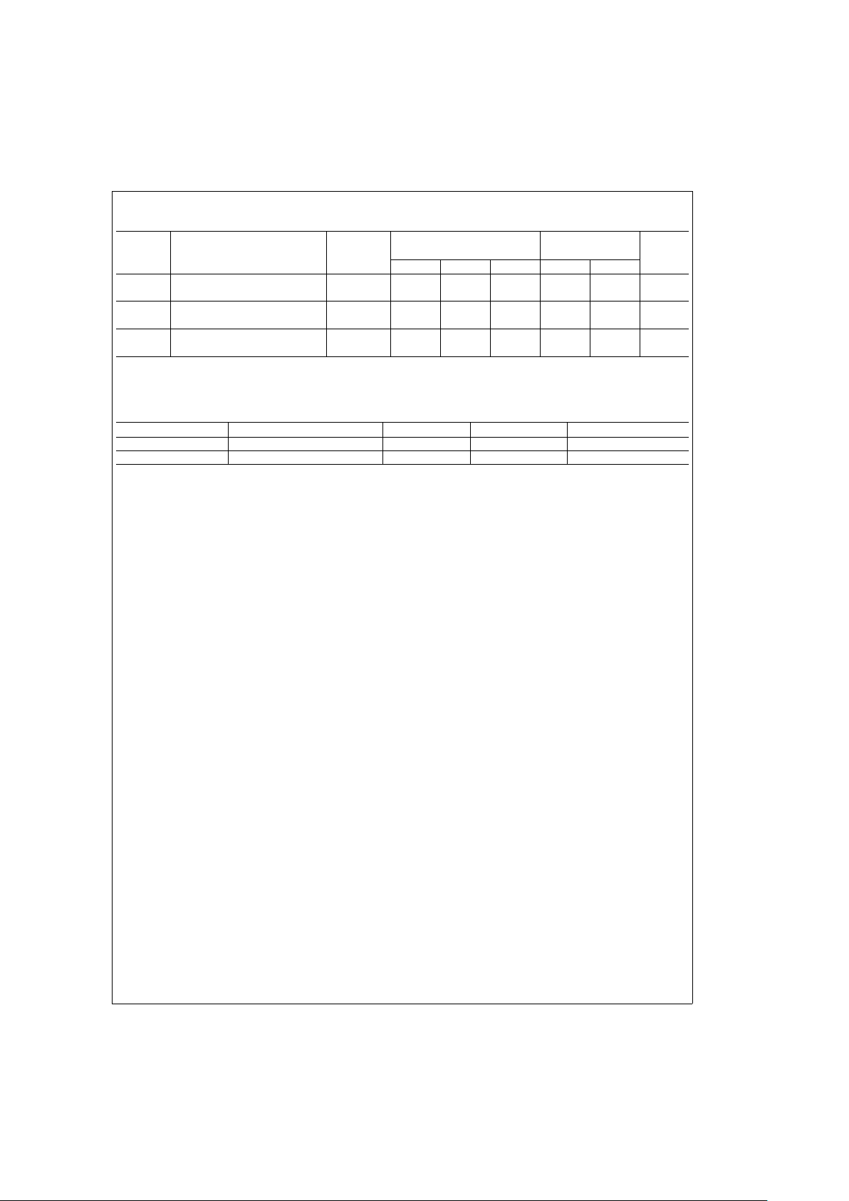
AC Electrical Characteristics
Symbol Parameter
V
CC
(V)
T
A
=
+25˚C T
A
=
−40˚ C to +85˚C
UnitsC
L
=
50 pF C
L
=
50 pF
Min Typ Max Min Max
t
PLH
Propagation Delay 2.7 1.5 5.4 12.7 1.0 14.0 ns
3.3
±
0.3 1.5 4.5 9.0 1.0 10.0
t
PHL
Propagation Delay 2.7 1.5 5.4 12.0 1.0 12.0 ns
3.3
±
0.3 1.5 4.5 8.5 1.0 9.5
t
OSHL
Output to Output Skew (Note 9) 2.7 1.0 1.5 1.5 ns
t
OSLH
Data to Output 3.3±0.3 1.0 1.5 1.5
Note 9: Skew is defined as the absolute value of the difference between the actual propagation delay for any two separate outputs of the same device. The specification applies to any outputs switching in the same direction, either HIGH to LOW (t
OSHL
) or LOW to HIGH (t
OSLH
). Parameter guaranteed by design.
Capacitance
Symbol Parameter Typ Units Conditions
C
IN
Input Capacitance 4.5 pF V
CC
=
Open
C
PD
(Note 10) Power Dissipation Capacitance 17 pF V
CC
=
3.3V
Note 10: CPDis measured at 10 MHz.
3 www.fairchildsemi.com
Page 4

4
Page 5
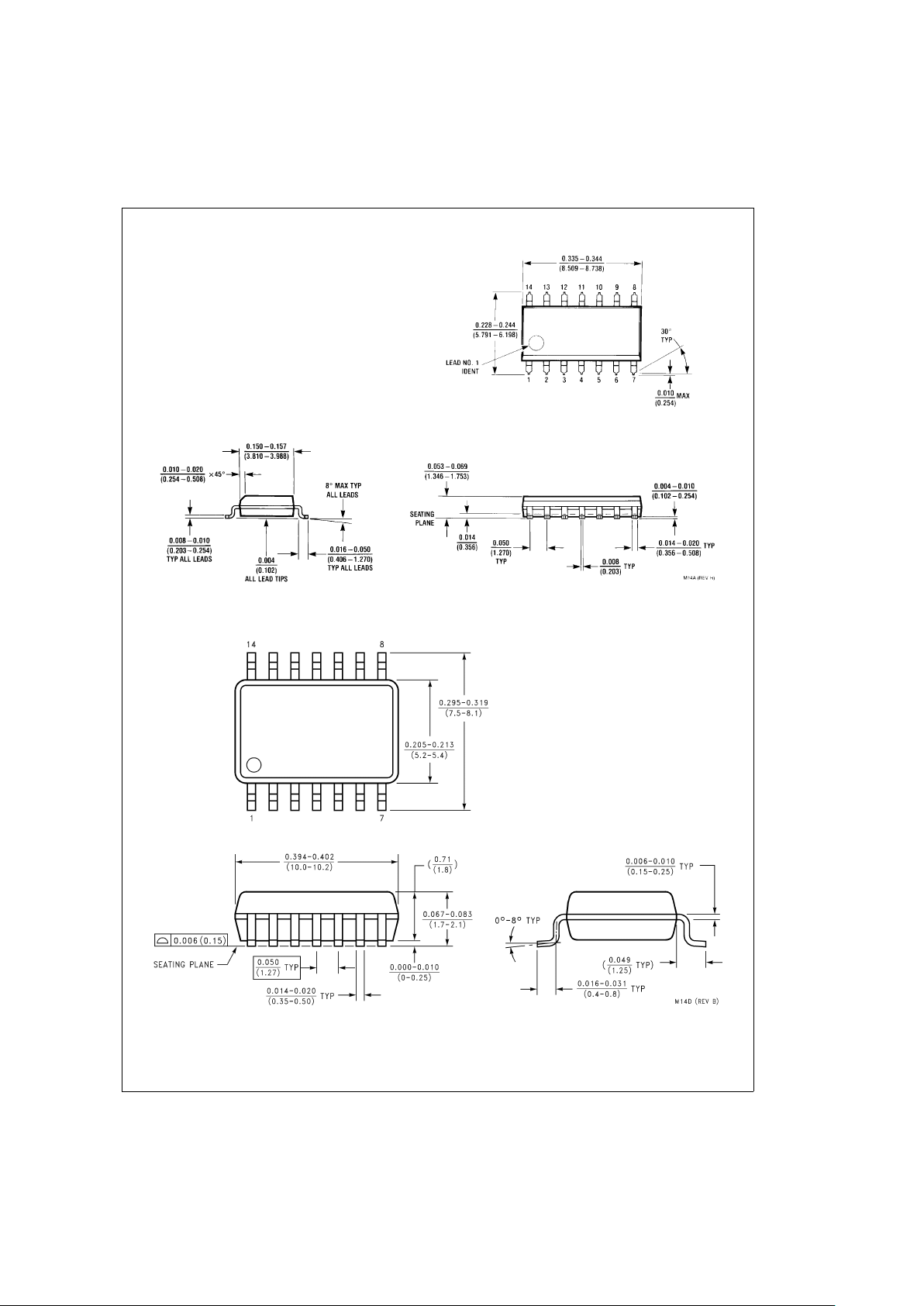
Physical Dimensions inches (millimeters) unless otherwise noted
14-Lead (0.150" Wide) Small Outline Package, SOIC JEDEC
Package Number M14A
14-Lead Molded Small Outline Package, SOIC EIAJ
Package Number M14D
5 www.fairchildsemi.com
Page 6

LIFE SUPPORT POLICY
FAIRCHILD’S PRODUCTS ARE NOT AUTHORIZED FOR USE AS CRITICAL COMPONENTS IN LIFE SUPPORT DEVICES OR SYSTEMS WITHOUT THE EXPRESS WRITTEN APPROVAL OF THE PRESIDENT OF FAIRCHILD SEMICONDUCTOR CORPORATION. As used herein:
1. Life support devices or systems are devices or systems which, (a) are intended for surgical implant into
the body, or (b) support or sustain life, and (c) whose
failure to perform when properly used in accordance
with instructions for use provided in the labeling, can
be reasonably expected to result in asignificant injury
to the user.
2. A critical component in any component of a life support
device or system whose failure to perform can be reasonably expected to cause the failure of the life support
device or system, or to affect itssafety or effectiveness.
Fairchild Semiconductor
Corporation
Americas
Customer Response Center
Tel: 1-888-522-5372
www.fairchildsemi.com
Fairchild Semiconductor
Europe
Fax: +49 (0) 1 80-530 85 86
Email: [email protected]
Deutsch Tel: +49 (0) 8 141-35-0
English Tel: +44 (0) 1 793-85-68-56
Italy Tel: +39 (0) 2 57 5631
Fairchild Semiconductor
Hong Kong Ltd.
13th Floor, Straight Block,
Ocean Centre, 5 Canton Rd.
Tsimshatsui, Kowloon
Hong Kong
Tel: +852 2737-7200
Fax: +852 2314-0061
National Semiconductor
Japan Ltd.
Tel: 81-3-5620-6175
Fax: 81-3-5620-6179
74LVQ04 Low Voltage Hex Inverter
Fairchild does not assume any responsibility for use of any circuitry described, no circuit patent licenses are implied and Fairchild reserves the right at any time without notice to change said circuitry and specifications.
 Loading...