

Page 1
INTEGRATED CIRCUITS
74LVC827A
10-bit buffer/line driver with 5-volt tolerant
inputs/outputs (3-State)
Poduct specification 1998 Sep 04
Page 2
Philips Semiconductors Product specification
10-bit buffer/line driver with 5-volt tolerant
inputs/outputs (3-State)
FEA TURES
•5-volt tolerant inputs/outputs, for interfacing with 5-volt logic
•Supply voltage range of 2.7V to 3.6V
•Complies with JEDEC standard no. 8-1A
•CMOS low power consumption
•Direct interface with TTL levels
•High impedance when V
QUICK REFERENCE DATA
GND = 0 V; T
SYMBOL
t
NOTES:
is used to determine the dynamic power dissipation (PD in µW)
1. C
PD
P
= CPD × V
D
fi = input frequency in MHz; CL = output load capacity in pF;
= output frequency in MHz; VCC = supply voltage in V;
f
o
(C
L
2. The condition is VI = GND to V
= 25°C; tr = tf ≤ 2.5 ns
amb
PHL/tPLH
C
I
C
PD
2
× fi (CL × V
CC
2
× V
× fo) = sum of the outputs.
CC
= 0V
CC
PARAMETER CONDITIONS TYPICAL UNIT
Propagation delay
An to Y
n
Input capacitance 5.0 pF
Power dissipation capacitance per buffer Notes 1 and 2 24 pF
2
× fo) where:
CC
CC
DESCRIPTION
The 74LVC827A is a high performance, low-power, low-voltage
Si-gate CMOS device and superior to most advanced CMOS
compatible TTL families.
Inputs can be driven from either 3.3V or 5.0V devices. In 3-state
operation, outputs can handle 5V. This feature allows the use of
these devices as translators in a mixed 3.3V/5V environment.
The 74LVC827A is a10-bit buf fer/line driver with 3-State outputs The
3-State outputs are controlled by the output enable inputs OE
OE
A HIGH on OE
OFF-state.
CL = 50 pF;
VCC = 3.3 V
74L VC827A
and
.
2
causes the outputs to assume a high impedance
n
4 ns
1
ORDERING INFORMATION
PACKAGES TEMPERATURE RANGE OUTSIDE NORTH AMERICA NORTH AMERICA PKG. DWG. #
24-Pin Plastic SO –40°C to +85°C 74LVC827A D 74LVC827A D SOT137-1
24-Pin Plastic SSOP Type II –40°C to +85°C 74LVC827A DB 74LVC827A DB SOT340-1
24-Pin Plastic TSSOP Type I –40°C to +85°C 74LVC827A PW 7LVC827APW DH SOT355-1
PIN DESCRIPTION
PIN NUMBER SYMBOL NAME AND FUNCTION
1, 13 OE1, OE
2, 3, 4, 5, 6,
7, 8, 9, 10, 11
12 GND Ground (0 V)
23, 22, 21, 20,
19, 18, 17, 16,
15, 14
24 V
A0 to A9Data inputs
Y0 to Y9Bus outputs
CC
Output enable input
2
(active LOW)
Positive supply voltage
FUNCTION TABLE
INPUTS OUTPUTS
OE
1
L L L L
L L H H
X H X Z
H X X Z
H = HIGH voltage level
L = LOW voltage level
X = Don’t care
Z = high impedance OFF-state
OE
2
An Yn
1998 Sep 04 853–21 17 19969
2
Page 3
Philips Semiconductors Product specification
10-bit buffer/line driver with 5-volt tolerant
inputs/outputs (3-State)
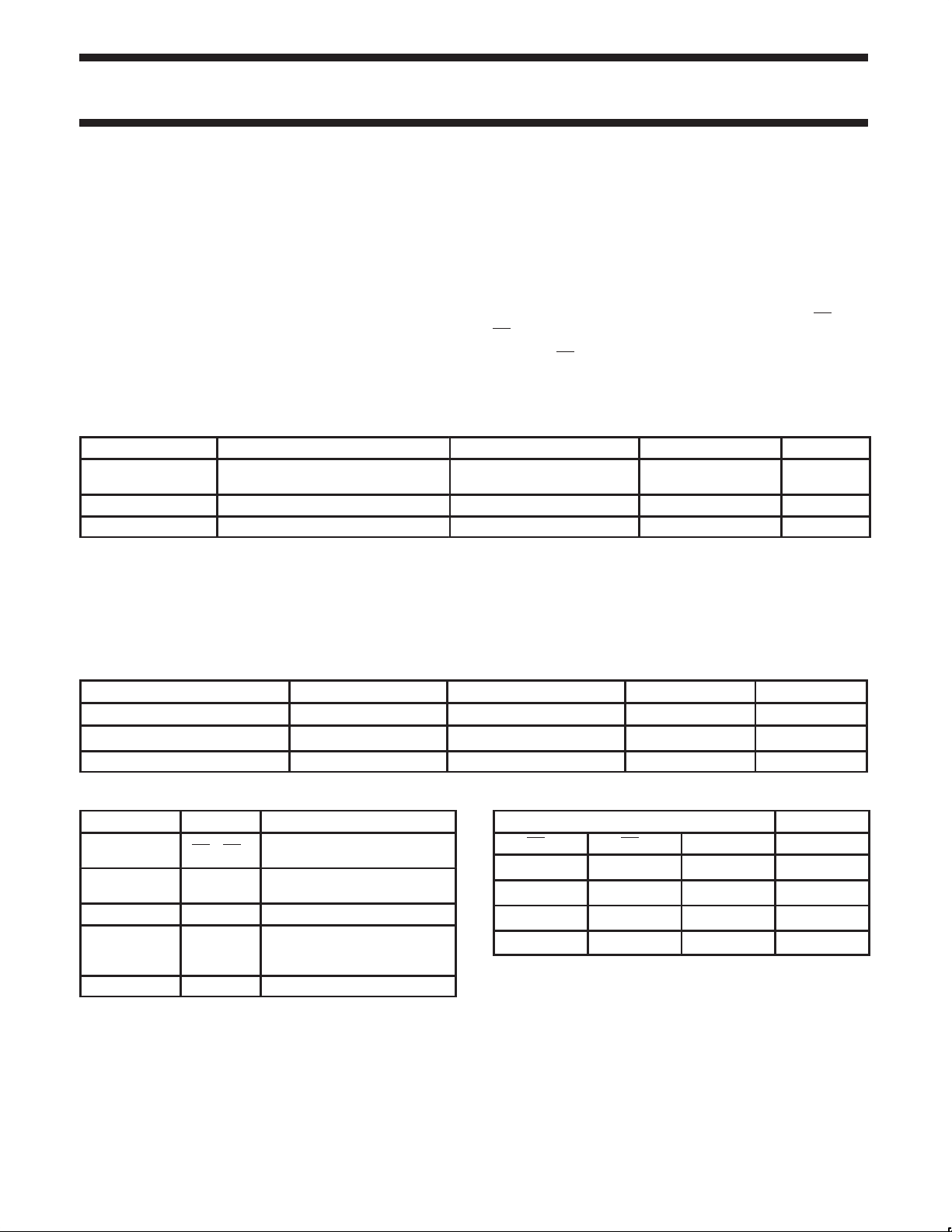
PIN CONFIGURATION
OE
GND
1
1
A
2
0
3
A
1
4
A
2
A
5
3
A
6
4
A
7
5
8
A
6
9
A
7
10
A
8
11
A
9
12
24
V
CC
23
Y
0
22
Y
1
Y
21
2
Y
20
3
Y
19
4
18
Y
5
17
Y
6
Y
16
7
Y
15
8
Y
14
9
13
OE
2
LOGIC SYMBOL
2
3
4
5
6
7
8
9
74LVC827A
A
0
A
1
A
2
A
3
A
4
A
5
A
6
A
7
Y
0
23
Y
1
22
Y
2
21
Y
3
20
Y
4
19
Y
5
18
Y
6
17
Y
7
16
LOGIC SYMBOL (IEEE/IEC)
1
&
13
2
3
4
5
6
7
8
9
10
11
EN
SA00426
A
OE
OE
8
A
9
1
2
10
11
1
13
23
22
21
20
19
18
17
16
15
14
Y
8
Y
9
SA00427
15
14
1998 Sep 04
SA00428
3
Page 4
Philips Semiconductors Product specification
SYMBOL
PARAMETER
CONDITIONS
UNIT
V
V
O
10-bit buffer/line driver with 5-volt tolerant
inputs/outputs (3-State)
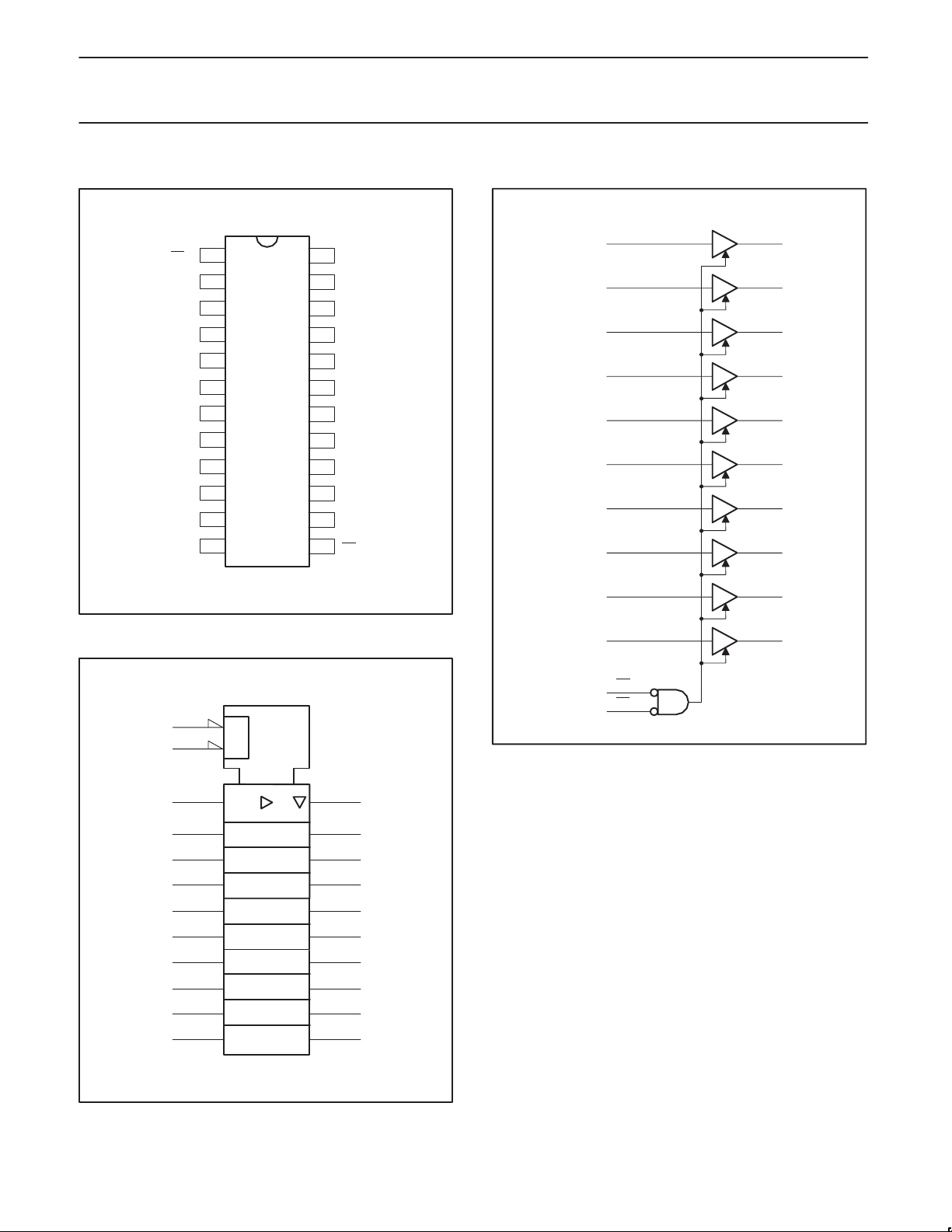
FUNCTIONAL DIAGRAM
A
0
2
A
1
3
A
2
4
A
3
5
A
4
6
A
5
7
A
6
8
A
7
9
Y
0
23
Y
1
22
Y
2
21
Y
3
20
Y
4
19
Y
5
18
Y
6
17
Y
7
16
74LVC827A
A
8
10
A
9
11
OE
1
1
OE
13
2
Y
8
Y
9
SA00429
15
14
RECOMMENDED OPERA TING CONDITIONS
DC supply voltage (for max. speed performance) 2.7 3.6
DC supply voltage (for low-voltage applications) 1.2 3.6
DC Input voltage range 0 5.5 V
I
DC output voltage range; output HIGH or LOW
state
DC output voltage range; output 3-State 0 5.5
Operating ambient temperature range in free-air –40 +85 °C
Input rise and fall times
f
T
CC
V
V
amb
tr, t
VCC = 1.2 to 2.7V
VCC = 2.7 to 3.6V
LIMITS
MIN MAX
0 V
0
0
CC
20
10
V
ns/V
1998 Sep 04
4
Page 5

Philips Semiconductors Product specification
V
V
mW
VIHHIGH level Input voltage
V
VILLOW level Input voltage
V
VOHHIGH level output voltage
V
10-bit buffer/line driver with 5-volt tolerant
74LVC827A
inputs/outputs (3-State)
ABSOLUTE MAXIMUM RATINGS
In accordance with the Absolute Maximum Rating System (IEC 134)
Voltages are referenced to GND (ground = 0V)
SYMBOL
V
CC
I
IK
V
I
OK
DC supply voltage –0.5 to +6.5 V
DC input diode current VI t0 –50 mA
DC input voltage Note 2 –0.5 to +6.5 V
I
DC output diode current V
DC output voltage; output HIGH or LOW state Note 2 –0.5 to VCC +0.5
O
DC output voltage; output 3-State Note 2 –0.5 to 6.5
I
GND
I
O
T
stg
DC output source or sink current VO = 0 to V
, I
DC VCC or GND current
CC
Storage temperature range –65 to +150 °C
Power dissipation per package
P
TOT
– plastic mini-pack (SO) above +70°C derate linearly with 8 mW/K 500
– plastic shrink mini-pack (SSOP and TSSOP) above +60°C derate linearly with 5.5 mW/K 500
NOTES:
1. Stresses beyond those listed may cause permanent damage to the device. These are stress ratings only and functional operation of the
device at these or any other conditions beyond those indicated under “recommended operating conditions” is not implied. Exposure to
absolute-maximum-rated conditions for extended periods may affect device reliability .
2. The input and output voltage ratings may be exceeded if the input and output current ratings are observed.
PARAMETER CONDITIONS RATING UNIT
1
uVCC or VO t 0
O
CC
"50
"50
"100
mA
mA
mA
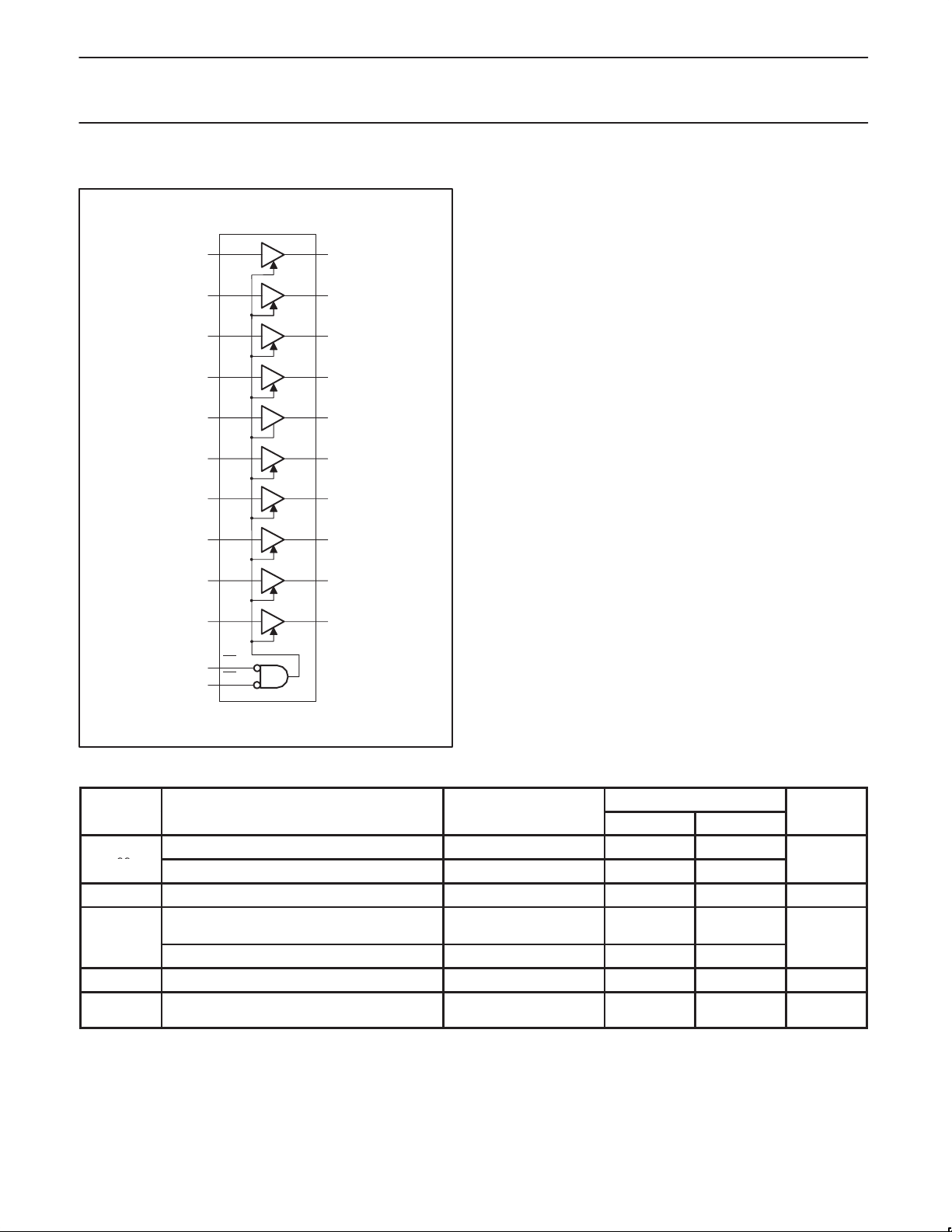
DC ELECTRICAL CHARACTERISTICS
Over recommended operating conditions voltages are referenced to GND (ground = 0V)
LIMITS
SYMBOL PARAMETER TEST CONDITIONS Temp = -40°C to +85°C UNIT
MIN TYP1MAX
p
p
VCC = 1.2V V
VCC = 2.7 to 3.6V 2.0
VCC = 1.2V GND
VCC = 2.7 to 3.6V 0.8
VCC = 2.7V; VI = VIH or VIL;IO = –12mA VCC*0.5
p
VCC = 3.0V; VI = VIH or VIL;IO = –100µA VCC*0.2 V
VCC = 3.0V; VI = VIH or V
VCC = 3.0V; VI = VIH or V
= –18mA VCC*0.6
IL;IO
= –24mA VCC*0.8
IL;IO
VCC = 2.7V; VI = VIH or VIL;IO = 12mA 0.40
V
LOW level output voltage
OL
VCC = 3.0V; VI = VIH or VIL;IO = 100µA 0.20
VCC = 3.0V; VI = VIH or V
= 24mA 0.55
IL;IO
NOTES:
1. All typical values are at V
2. The specified overdrive current at the data input forces the data input to the opposite logic input state.
= 3.3V and T
CC
amb
= 25°C.
CC
CC
V
1998 Sep 04
5
Page 6

Philips Semiconductors Product specification
IIInput leakage current
V
V
GND
Not for I/O pins
"0.1
"5
A
10-bit buffer/line driver with 5-volt tolerant
74LVC827A
inputs/outputs (3-State)
DC ELECTRICAL CHARACTERISTICS
Over recommended operating conditions voltages are referenced to GND (ground = 0V)
SYMBOL PARAMETER TEST CONDITIONS Temp = -40°C to +85°C UNIT
p
I
I
I
CC
∆I
3-State output OFF-state current VCC = 3.6V; VI = VIH or VIL;VO = 5.5V or GND 0.1
OZ
Power off leakage supply VCC = 0.0V; V
off
Quiescent supply current VCC = 3.6V; VI = VCC or GND; IO = 0 0.1 10 µA
Additional quiescent supply current
CC
per input pin
NOTES:
1. All typical values are at V
2. The specified overdrive current at the data input forces the data input to the opposite logic input state.
= 3.3V and T
CC
AC CHARACTERISTICS
GND = 0V; tr = tf v 2.5ns; CL = 50pF; RL = 500Ω; T
SYMBOL PARAMETER WAVEFORM VCC = 3.3V ±0.3V VCC = 2.7V VCC = 1.2V UNIT
t
PHL
t
PLH
t
PZH
t
PZL
t
PHZ
t
PLZ
NOTE:
1. Unless otherwise stated, all typical values are at V
Propagation delay
1An to 1Yn;
2An to 2Y
n
3-State output enable time
OE1 to 1Yn;
OE2 to 2Y
n
3-State output disable time
OE1 to 1Yn;
OE2 to 2Y
n
(Continued)
LIMITS
MIN TYP1MAX
;
= 3.6V;
CC
= 5.5V or
I
or VO = 5.5V 0.1
I
VCC = 2.7V to 3.6V; VI = VCC –0.6V; IO = 0 5 500 µA
= 25°C.
amb
= –40°C to +85°C.
amb
MIN TYP1MAX MIN MAX TYP
Figures 1, 3 1.5 4.0 6.7 1.5 7.1 15 ns
Figures 2, 3 1.5 5.4 8.5 1.5 9.5 25 ns
Figures 2, 3 1.5 4.0 6.7 1.5 7.3 11 ns
= 3.3V and T
CC
amb
= 25°C.
p
LIMITS
"5
"10
µ
µA
µA
AC WAVEFORMS
VM = 1.5V at VCC w 2.7V; VM = 0.5 VCC at VCC t 2.7V.
VOL and VOH are the typical output voltage drop that occur with the
output load.
V
= VOL + 0.3V at VCC w 2.7V; VX = VOL + 0.1 VCC at VCC t 2.7V
X
V
= VOH –0.3V at VCC w 2.7V; VY = VOH – 0.1 VCC at VCC t 2.7V
Y
V
I
A
INPUT
n
GND
t
PHL
V
OH
OUTPUT
Y
n
V
OL
Figure 1. The input (An) to output (Yn) propagation delays.
1998 Sep 04
V
M
t
PLH
V
M
SA00431
6
V
I
OEn INPUT
GND
V
OUTPUT
LOW–to–OFF
OFF–to–LOW
V
V
OH
OUTPUT
HIGH–to–OFF
OFF–to–HIGH
GND
CC
OL
V
M
t
PLZ
t
outputs
enabled
PHZ
V
X
V
Y
outputs
disabled
Figure 2. 3-State enable and disable times.
t
PZL
t
PZH
V
M
V
M
outputs
enabled
SA00430
Page 7

Philips Semiconductors Product specification
10-bit buffer/line driver with 5-volt tolerant
inputs/outputs (3-State)
TEST CIRCUIT
S
1
2 x V
V
CC
PULSE
GENERATOR
V
I
R
T
V
CC
2.7V V
2.7V – 3.6V 2.7V
V
CC
D.U.T.
I
V
O
C
L
t
PLH/tPHL
t
PLZ/tPZL
t
PHZ/tPZH
Figure 3. Load circuitry for switching times.
50pF
Test S
2 x V
500Ω
500Ω
1
Open
CC
GND
Open
GND
SY00003
CC
74LVC827A
1998 Sep 04
7
Page 8

Philips Semiconductors Product specification
10-bit buffer/line driver with 5-volt tolerant
inputs/outputs (3-State)
SO24: plastic small outline package; 24 leads; body width 7.5 mm SOT137-1
74LVC827A
1998 Sep 04
8
Page 9

Philips Semiconductors Product specification
10-bit buffer/line driver with 5-volt tolerant
inputs/outputs (3-State)
SSOP24: plastic shrink small outline package; 24 leads; body width 5.3 mm SOT340-1
74LVC827A
1998 Sep 04
9
Page 10

Philips Semiconductors Product specification
10-bit buffer/line driver with 5-volt tolerant
inputs/outputs (3-State)
TSSOP24: plastic thin shrink small outline package; 24 leads; body width 4.4 mm SOT355-1
74LVC827A
1998 Sep 04
10
Page 11

Philips Semiconductors Product specification
10-bit buffer/line driver with 5-volt tolerant
inputs/outputs (3-State)
NOTES
74LVC827A
1998 Sep 04
11
Page 12

Philips Semiconductors Product specification
10-bit buffer/line driver with 5-volt tolerant
inputs/outputs (3-State)
Data sheet status
Data sheet
status
Objective
specification
Preliminary
specification
Product
specification
Product
status
Development
Qualification
Production
Definition
This data sheet contains the design target or goal specifications for product development.
Specification may change in any manner without notice.
This data sheet contains preliminary data, and supplementary data will be published at a later date.
Philips Semiconductors reserves the right to make chages at any time without notice in order to
improve design and supply the best possible product.
This data sheet contains final specifications. Philips Semiconductors reserves the right to make
changes at any time without notice in order to improve design and supply the best possible product.
[1]
74LVC827A
[1] Please consult the most recently issued datasheet before initiating or completing a design.
Definitions
Short-form specification — The data in a short-form specification is extracted from a full data sheet with the same type number and title. For
detailed information see the relevant data sheet or data handbook.
Limiting values definition — Limiting values given are in accordance with the Absolute Maximum Rating System (IEC 134). Stress above one
or more of the limiting values may cause permanent damage to the device. These are stress ratings only and operation of the device at these or
at any other conditions above those given in the Characteristics sections of the specification is not implied. Exposure to limiting values for extended
periods may affect device reliability.
Application information — Applications that are described herein for any of these products are for illustrative purposes only. Philips
Semiconductors make no representation or warranty that such applications will be suitable for the specified use without further testing or
modification.
Disclaimers
Life support — These products are not designed for use in life support appliances, devices or systems where malfunction of these products can
reasonably be expected to result in personal injury . Philips Semiconductors customers using or selling these products for use in such applications
do so at their own risk and agree to fully indemnify Philips Semiconductors for any damages resulting from such application.
Right to make changes — Philips Semiconductors reserves the right to make changes, without notice, in the products, including circuits, standard
cells, and/or software, described or contained herein in order to improve design and/or performance. Philips Semiconductors assumes no
responsibility or liability for the use of any of these products, conveys no license or title under any patent, copyright, or mask work right to these
products, and makes no representations or warranties that these products are free from patent, copyright, or mask work right infringement, unless
otherwise specified.
Philips Semiconductors
811 East Arques Avenue
P.O. Box 3409
Sunnyvale, California 94088–3409
Telephone 800-234-7381
Copyright Philips Electronics North America Corporation 1998
All rights reserved. Printed in U.S.A.
print code Date of release: 08-98
Document order number: 9397-750-04521
yyyy mmm dd
12
 Loading...