

Page 1

INTEGRATED CIRCUITS
74LVC169
Presettable synchronous 4-bit up/down
binary counter
specification
Supersedes data of 1996 Aug 23
IC24 Data Handbook
1998 May 20
Page 2
Philips Semiconductors Product specification
Presettable synchronous 4-bit up/down
binary counter
FEA TURES
•Wide supply voltage range of 1.2 V to 3.6 V
•In accordance with JEDEC standard no. 8-1A
•Inputs accept voltages up to 5.5 V
•CMOS low power consumption
•Direct interface with TTL levels
•Synchronous counting and loading
•Up/down counting
•Modular 16 binary counter
•Two count enable inputs for n-bit cascading
•Built-in lookahead carry capability
•Presettable for programmable operation
•Positive-edge triggered clock
DESCRIPTION
The 74LVC169 is a high-performance, low-power, low-voltage,
Si-gate CMOS device and superior to most advanced CMOS
compatible TTL families.
74L VC169
The 74LVC169 is a synchronous presettable binary counter which
features an internal lookahead carry and can be used for high-speed
counting. Synchronous operation is provided by having all flip-flops
clocked simultaneously on the positive-going edge of the clock (CP).
The outputs (Q
LOW level. A LOW level at the parallel enable input (PE) disables
the counting action and causes the data at the data inputs
(D
to D3) to be loaded into the counter on the positive-going edge
0
of the clock (provided that the set-up and hold time requirements for
PE are met). Preset takes place regardless of the levels at count
enable inputs (CEP and CET). A low level at the master reset input
(MR) sets all four outputs of the flip-flops (Q
after the next positive-going transition on the clock (CP) input
(provided that the set-up and hold time requirements for PE are
met).
This action occurs regardless of the levels at CP, PE
inputs This synchronous reset feature enables the designer to
modify the maximum count with only one external NAND gate.
The lookahead carry simplifies serial cascading of the counters.
Both count enable inputs (CEP and CET) must be HIGH to count.
The CET input is fed forward to enable the terminal count output
(TC). The TC output thus enabled will produce a HIGH output pulse
of a duration approximately equal to a HIGH level output of Q
pulse can be used to enable the next cascaded stage. The
maximum clock frequency for the cascaded counters is determined
by the CP to TC propagation delay and CEP to CP set-up time,
according to the following formula:
to Q3) of the counters may be preset to a HIGH or
0
to Q3) to LOW level
0
, CET and CEP
. This
0
_______________________________
f
=
max
tp
(CP to TC) + tSU (CEP to CP)
(max)
1
QUICK REFERENCE DATA
GND = 0V; T
SYMBOL
t
PHL/tPLH
f
MAX
C
I
C
PD
NOTES:
1. C
is used to determine the dynamic power dissipation (PD in µW)
PD
= CPD x V
P
D
f
= input frequency in MHz; CL = output load capacity in pF;
i
= output frequency in MHz; VCC = supply voltage in V;
f
o
Σ (C
L
2. The condition is V
= 25°C; TR = TF 2.5ns
amb
Propagation delay
CP to Q
CP to TC
CET to TC
maximum clock frequency 200 MHz
input capacitance 5.0 pF
power dissipation capacitance per gate notes 1 and 2 42 pF
2
x fi +Σ (CL x V
CC
2
x V
x f
CC
= sum of the outputs
o )
= GND to V
1
PARAMETER CONDITIONS TYPICAL UNIT
CL = 50 pF
n
2
x f
CC
CC
where:
o )
VCC = 3.3V 5.0
6.5
5.3
ORDERING INFORMATION
PACKAGES TEMPERATURE RANGE OUTSIDE NORTH AMERICA NORTH AMERICA DWG NUMBER
16-Pin Plastic SO –40°C to +85°C 74LVC169 D 74LVC169 D SOT109-1
16-Pin Plastic SSOP Type II –40°C to +85°C 74LVC169 DB 74LVC169 DB SOT338-1
16-Pin Plastic TSSOP Type I –40°C to +85°C 74LVC169 PW 74LVC169PW DH SOT403-1
ns
1998 May 20 853-1866 19421
2
Page 3
Philips Semiconductors Product specification
Presettable synchronous 4-bit up/down
binary counter
PIN CONFIGURATION
U/D
CP
D
D
D
D
CEP
GND
LOGIC SYMBOL
1
2
3
0
4
1
5
2
6
3
7
3456
16
15
14
13
12
11
10
98
SF00766
V
TC
Q
Q
Q
Q
CET
PE
CC
0
1
2
3
74LVC169
PIN DESCRIPTION
PIN NUMBER SYMBOL FUNCTION
1 U/D up/down control input
2 CP
3,4,5,6 D0 to D
7 CEP
8 GND ground (0V)
9 PE
10 CET
14,13,12,11 Q0 to Q
15 TC
16 V
CC
clock input (LOW-to-HIGH,
edge-triggered)
data inputs
3
count enable inputs (active
LOW)
parallel enable input
(active LOW)
count enable carry input
(active LOW)
flip-flop outputs
3
terminal count output
(active LOW)
positive supply voltage
10
VCC = Pin 16
GND = Pin 8
D
PE
9
1
U/D
CP
2
CEP
7
CET
0D1D2D3
Q0Q1Q2Q
TC
3
11121314
15
SF00786
LOGIC SYMBOL (IEEE/IEC)
9
1
10
7
2
3
4
5
6
CTR DIV 16
M1 [LOAD]
M2 [COUNT]
M3 [UP]
M4 [DOWN]
G5
G6
2, 3, 5, 6+/C7
2, 4, 5, 6–
1, 7D
[1]
[2]
[4]
[8]
3, 5 CT=15
4, 5 CT=0
15
14
13
12
11
SF00787
1998 May 20
3
Page 4
Philips Semiconductors Product specification
Presettable synchronous 4-bit up/down
binary counter
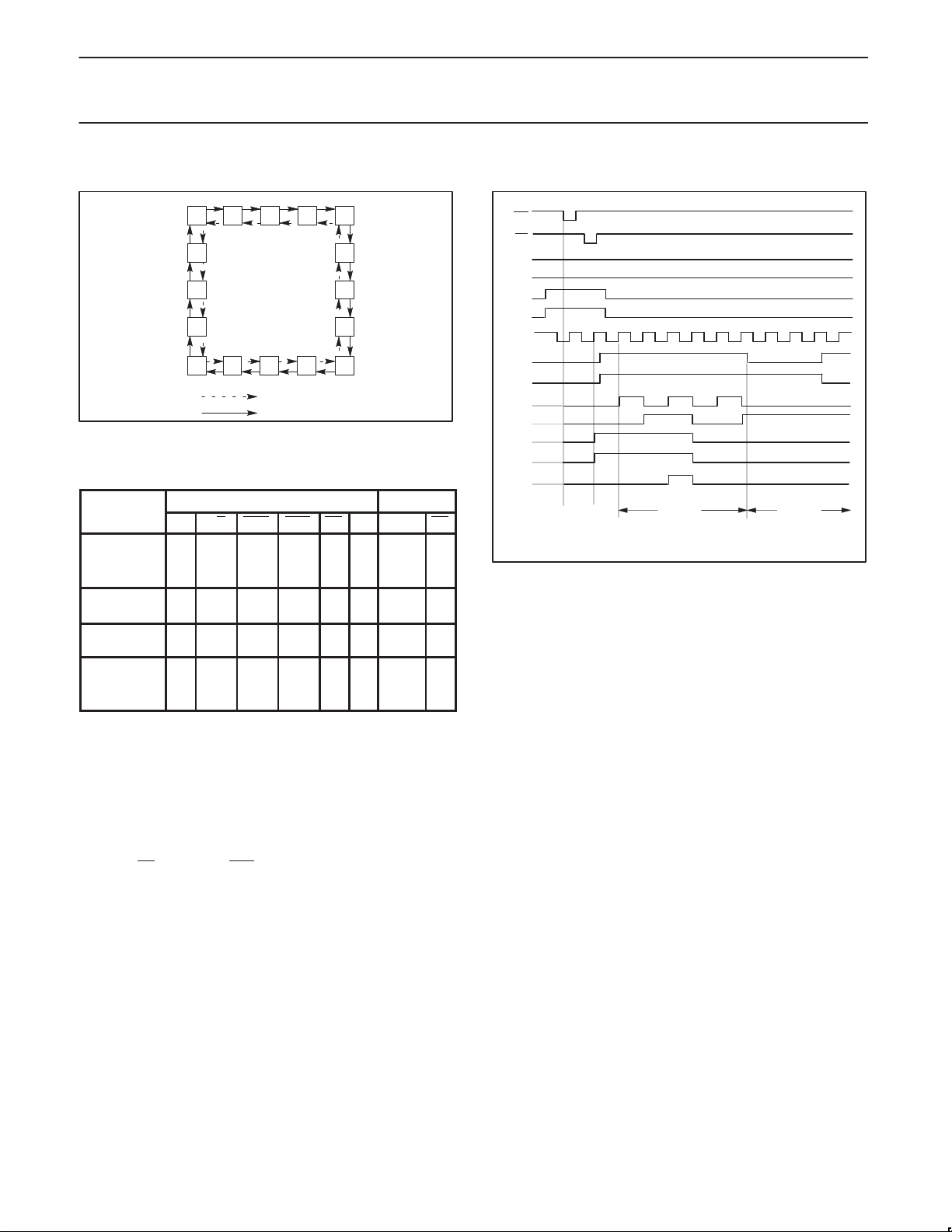
STATE DIAGRAM
01234
15
14
13
COUNT DOWN
COUNT UP
FUNCTION TABLE
OPERATING
MODES
Parallel load
(Dn→Qn)
CP U/D CEP CET PE DnQnTC
↑ X X X l l L *
↑
Count Up
(increment)
Count Down
(decrement)
Hold
(do nothing)
↑
↑
↑
↑
H = High voltage level steady state
h = High voltage level one setup time prior to the Low-to-High
clock transition
L = Low voltage level steady state
l = Low voltage level one setup time prior to the Low-to-High
clock transition
q = Lower case letters indicate the state of the referenced output
prior to the Low-to-High clock transition
X = Don’t care
↑ = Low-to-High clock transition
* = The TC
is Low when CET is Low and the counter is at
Terminal Count.
Terminal Count Up is (HHHH) and Terminal Count Down is
(LLLL).
INPUTS OUTPUTS
X X X X X H *
h l l h X
l l l h X
X h X h X q
X X X h X q
5
6
7
89101112
SF00788
Count
Up
Count
Down
n
H
n
74LVC169
TYPICAL TIMING SEQUENCE
MR
PE
D0
D1
D2
D3
CP
CEP
CET
Q0
Q1
Q2
Q3
TC
Typical timing sequence: reset outputs to zero; preset to binary
*
twelve; count to thirteen, fourteen, fifteen, zero, one, and two;
inhibit
*
*
12 13 14 15 0 1 2
RESET PRESET
INHIBITCOUNT
SY00069
1998 May 20
4
Page 5
Philips Semiconductors Product specification
Presettable synchronous 4-bit up/down
binary counter
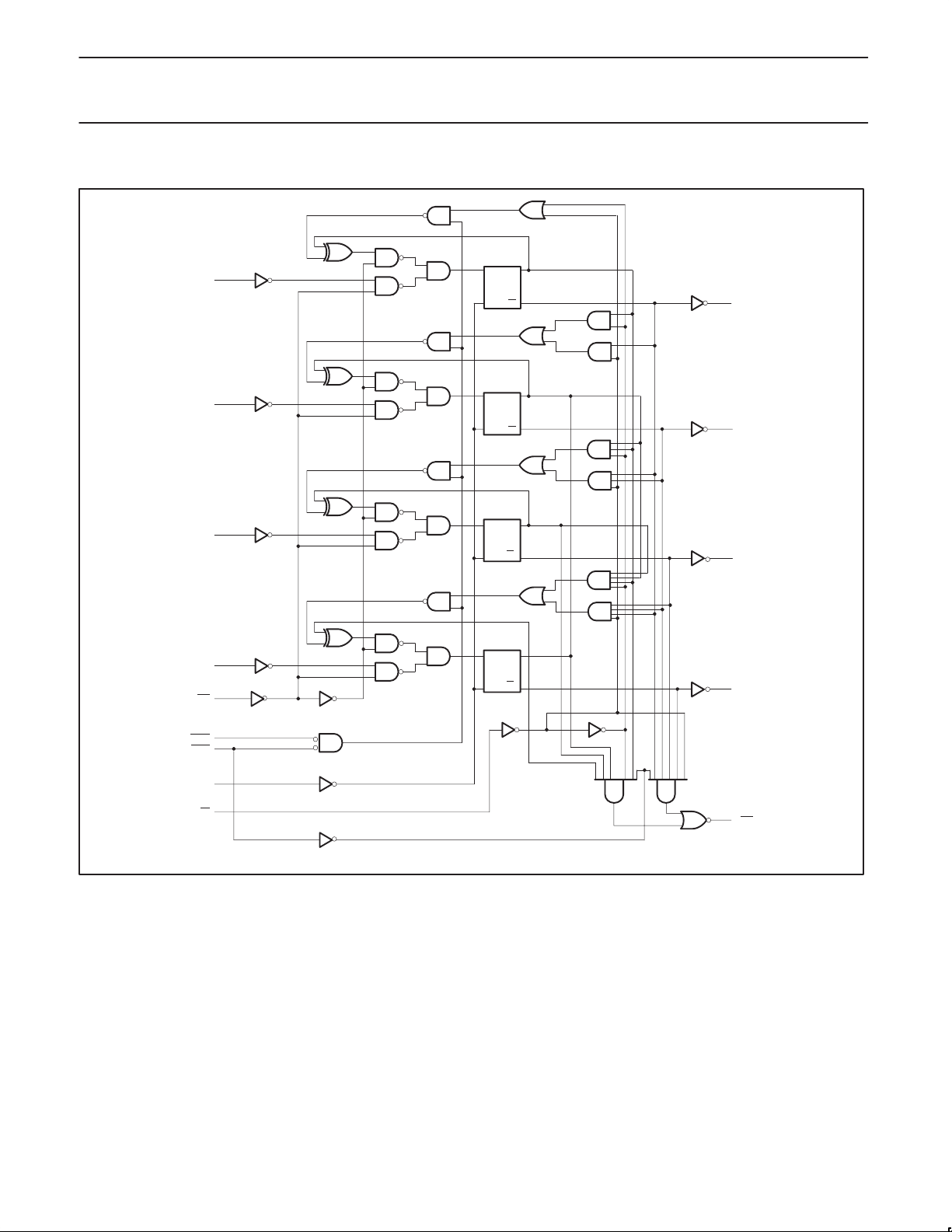
LOGIC DIAGRAM
3
D
0
4
D
1
5
D
2
DCPQ
DCPQ
DCPQ
74LVC169
Q
Q
Q
14
Q
0
13
Q
1
12
Q
2
VCC= Pin 16
GND = Pin 8
D
PE
CEP
CET
CP
U/D
6
3
9
7
10
2
1
DCPQ
Q
11
15
SF00789
Q
3
TC
1998 May 20
5
Page 6

Philips Semiconductors Product specification
SYMBOL
PARAMETER
CONDITIONS
UNIT
V
V
P
TOT
Presettable synchronous 4-bit up/down
binary counter
APPLICATION
CP
U/D
PE
D
0D1D2D3
PE
U/D
CP
CEP
CET
Q0Q1Q2Q
LEAST SIGNIFICANT
4-BIT COUNTER
TC
3
RECOMMENDED OPERATING CONDITIONS
DC supply voltage (for max. speed performance) 2.7 3.6
DC supply voltage (for low-voltage applications) 1.2 3.6
DC input voltage range 0 5.5 V
I
DC output voltage range 0 V
O
Operating free-air temperature range –40 +85 °C
Input rise and fall times
f
T
CC
V
V
amb
tr, t
D
0D1D2D3
PE
U/D
CP
CEP
CET
Q0Q1Q2Q
Synchronous multistage counting scheme
74LVC169
D
0D1D2D3
PE
U/D
TC
3
CP
CEP
CET
Q0Q1Q2Q
TC
3
MIN MAX
VCC = 1.2 to 2.7V
VCC = 2.7 to 3.6V
0
0
PE
U/D
CP
CEP
CET
LIMITS
D
0D1D2D3
Q0Q1Q2Q
MOST SIGNIFICANT
4-BIT COUNTER
CC
20
10
TC
3
SF00790
V
ns/V
ABSOLUTE MAXIMUM RATINGS
1
In accordance with the Absolute Maximum Rating System (IEC 134)
Voltages are referenced to GND (ground = 0V)
SYMBOL
V
CC
I
IK
V
I
I
OK
V
O
I
O
I
, I
GND
CC
T
stg
DC supply voltage –0.5 to +6.5 V
DC input diode current VI 0 –50 mA
DC input voltage Note 2 –0.5 to +5.5 V
DC output diode current V
DC output voltage Note 2 –0.5 to VCC +0.5 V
DC output source or sink current VO = 0 to V
DC VCC or GND current 100 mA
Storage temperature range –65 to +150 °C
PARAMETER CONDITIONS RATING UNIT
VCC or VO 0 50 mA
O
CC
50 mA
Power dissipation per package
– plastic mini-pack (SO) above +70°C derate linearly with 8 mW/K 500
– plastic shrink mini-pack (SSOP and
TSSOP)
above +60°C derate linearly with 5.5 mW/K 500
mW
NOTES:
1. Stresses beyond those listed may cause permanent damage to the device. These are stress ratings only and functional operation of the
device at these or any other conditions beyond those indicated under “recommended operating conditions” is not implied. Exposure to
absolute-maximum-rated conditions for extended periods may affect device reliability .
2. The input and output voltage ratings may be exceeded if the input and output current ratings are observed.
1998 May 20
6
Page 7

Philips Semiconductors Product specification
VIHHIGH level Input voltage
V
VILLOW level Input voltage
V
VOHHIGH level output voltage
V
IIInput leakage current
V
V
GND
0.1
5µA
Presettable synchronous 4-bit up/down
binary counter
DC ELECTRICAL CHARACTERISTICS
Over recommended operating conditions voltages are referenced to GND (ground = 0V)
SYMBOL PARAMETER TEST CONDITIONS Temp = -40°C to +85°C UNIT
MIN TYP1MAX
V
LOW level output voltage
OL
p
I
CC
∆I
Quiescent supply current VCC = 3.6V; VI = VCC or GND; IO = 0 0.1 10 µA
Additional quiescent supply current per
CC
input pin
NOTES:
1. All typical values are at V
p
p
p
= 3.3V and T
CC
amb
= 25°C.
VCC = 1.2V V
VCC = 2.7 to 3.6V 2.0
VCC = 1.2V GND
VCC = 2.7 to 3.6V 0.8
VCC = 2.7V; VI = VIH or VIL; IO = –12mA VCC0.5
VCC = 3.0V; VI = VIH or VIL; IO = –100µA VCC0.2 V
VCC = 3.0V; VI = VIH or V
VCC = 3.0V; VI = VIH or V
IO = –12mA VCC0.6
IL;
IO = –24mA VCC1.0
IL;
VCC = 2.7V; VI = VIH or VIL; IO = 12mA 0.40
VCC = 3.0V; VI = VIH or VIL; IO = 100µA GND 0.20
VCC = 3.0V; VI = VIH or V
;
= 3.6V;
CC
= 5.5V or
I
IO = 24mA 0.55
IL;
VCC = 2.7V to 3.6V; VI = VCC –0.6V; IO = 0 5 500 µA
CC
74LVC169
LIMITS
CC
V
1998 May 20
7
Page 8

Philips Semiconductors Product specification
LIMITS
Presettable synchronous 4-bit up/down
binary counter
AC CHARACTERISTICS
GND = 0 V; tr = tf 2.5 ns; CL = 50 pF; RL = 500; T
SYMBOL PARAMETER WAVEFORM VCC = 3.3V ±0.3V VCC = 2.7V VCC = 1.2V UNIT
W
su
su
su
su
propagation delay
CP to Q
n
propagation delay
CP to TC
propagation delay
CET
to TC
propagation delay
U/D
to TC
clock pulse width
HIGH or LOW
set-up time
D
to CP
n
set-up time
to CP
PE
set-up time
U/D
to CP
set-up time
, CET to CP
CEP
t
PHL/tPLH
t
PHL/tPLH
t
PHL/tPLH
t
PHL/tPLH
t
t
t
t
t
hold time
t
h
D
, PE, CEP, CET,
n
U/D to CP
f
max
maximum clock pulse
frequency
NOTE:
1. These typical values are measured at V
= 3.3V and T
CC
= –40C to +85C
amb
MIN. TYP
1
MAX. MIN. MAX. TYP
1 - 5.0 8.5 - 9.5 24 ns
1 - 6.5 10.8 - 12.8 30 ns
2 - 5.3 8.7 - 9.7 19 ns
4 - 5.7 9.5 - 10.5 24 ns
1 4.0 1.2 - 5.0 - - ns
3 2.5 1.0 - 3.0 - - ns
3 3.0 1.2 - 3.5 - - ns
5 5.5 2.8 - 6.5 - - ns
5 4.5 2.1 - 5.5 - - ns
3 and 5 0 2.5 - 0 - - ns
1 125 200 - 110 - - MHz
= 25°C.
amb
74LVC169
1998 May 20
8
Page 9

Philips Semiconductors Product specification
Presettable synchronous 4-bit up/down
binary counter
AC WAVEFORMS
VM = 1.5 V at VCC 2.7 V
VM = 0.5 S VCC at VCC < 2.7 V
V
and VOH are the typical output voltage drop that occur with the output load.
OL
1/f
MAX
V
I
CP INPUT
GND
V
OH
Qn, TC OUTPUT
V
OL
Waveform 1. Clock (CP) to outputs (Qn, TC) propagation
delays, the clock pulse width and the maximum clock
frequency .
CET
TC
Waveform 2. Input (CET) to output (TC) propagation delays
and output transition times.
U/D
TC
Waveform 3. Master reset (MR) pulse width, the master reset
to output (Q
clock (CP) removal times.
V
M
t
w
t
PHL
V
M
V
M
t
PHL
V
M
V
M
t
PHL
V
M
, TC) propagation delays and the master reset to
n
t
PLH
SY00071
V
M
t
PLH
V
M
SF00792
V
M
t
PLH
V
M
SF00793
74LVC169
V
I
PE
INPUT
GND
V
I
CP INPUT
GND
V
I
INPUT
D
n
GND
The shaded areas indicate when the input is permitted
to change for predictable output performance.
Waveform 4. Setup and hold times for the input (Dn) and
parallel enable input (PE
V
I
CEP, CET
INPUT
GND
V
I
CP INPUT
GND
NOTE: The shaded areas indicate when the input is permitted
to change for predictable output performance.
Waveform 5. CEP and CET setup and hold times.
TEST CIRCUIT
PULSE
GENERATOR
V
M
t
V
M
V
V
M
t
suth
V
I
R
t
SU
t
h
t
SU
t
h
SU
t
h
t
SU
t
h
M
SC00137
).
t
suth
V
M
V
CC
V
O
D.U.T.
T
C
L
50pF
V
M
SC00138
S
1
500Ω
500Ω
2 * V
Open
GND
CC
1998 May 20
SWITCH POSITION
TEST S
t
PLH/tPHL
1
Open
V
CC
< 2.7V V
Waveform 6. Load circuitry for switching times.
9
V
I
CC
2.7V2.7–3.6V
SV00903
Page 10

Philips Semiconductors Product specification
Presettable synchronous 4-bit up/down
binary counter
SO16: plastic small outline package; 16 leads; body width 3.9 mm SOT109-1
74LVC169
1998 May 20
10
Page 11

Philips Semiconductors Product specification
Presettable synchronous 4-bit up/down
binary counter
SSOP16: plastic shrink small outline package; 16 leads; body width 5.3 mm SOT338-1
74LVC169
1998 May 20
11
Page 12

Philips Semiconductors Product specification
Presettable synchronous 4-bit up/down
binary counter
TSSOP16: plastic thin shrink small outline package; 16 leads; body width 4.4 mm SOT403-1
74LVC169
1998 May 20
12
Page 13

Philips Semiconductors Product specification
Presettable synchronous 4-bit up/down
binary counter
NOTES
74LVC169
1998 May 20
13
Page 14

Philips Semiconductors Product specification
Presettable synchronous 4-bit up/down
binary counter
DEFINITIONS
Data Sheet Identification Product Status Definition
Objective Specification
Preliminary Specification
Product Specification
Philips Semiconductors and Philips Electronics North America Corporation reserve the right to make changes, without notice, in the products,
including circuits, standard cells, and/or software, described or contained herein in order to improve design and/or performance. Philips
Semiconductors assumes no responsibility or liability for the use of any of these products, conveys no license or title under any patent, copyright,
or mask work right to these products, and makes no representations or warranties that these products are free from patent, copyright, or mask
work right infringement, unless otherwise specified. Applications that are described herein for any of these products are for illustrative purposes
only. Philips Semiconductors makes no representation or warranty that such applications will be suitable for the specified use without further testing
or modification.
Formative or in Design
Preproduction Product
Full Production
This data sheet contains the design target or goal specifications for product development. Specifications
may change in any manner without notice.
This data sheet contains preliminary data, and supplementary data will be published at a later date. Philips
Semiconductors reserves the right to make changes at any time without notice in order to improve design
and supply the best possible product.
This data sheet contains Final Specifications. Philips Semiconductors reserves the right to make changes
at any time without notice, in order to improve design and supply the best possible product.
74LVC169
LIFE SUPPORT APPLICA TIONS
Philips Semiconductors and Philips Electronics North America Corporation Products are not designed for use in life support appliances, devices,
or systems where malfunction of a Philips Semiconductors and Philips Electronics North America Corporation Product can reasonably be expected
to result in a personal injury. Philips Semiconductors and Philips Electronics North America Corporation customers using or selling Philips
Semiconductors and Philips Electronics North America Corporation Products for use in such applications do so at their own risk and agree to fully
indemnify Philips Semiconductors and Philips Electronics North America Corporation for any damages resulting from such improper use or sale.
Philips Semiconductors
811 East Arques Avenue
P.O. Box 3409
Sunnyvale, California 94088–3409
Telephone 800-234-7381
Philips Semiconductors and Philips Electronics North America Corporation
register eligible circuits under the Semiconductor Chip Protection Act.
Copyright Philips Electronics North America Corporation 1998
All rights reserved. Printed in U.S.A.
print code Date of release: 05-96
Document order number: 9397-750-04498
 Loading...