

Datasheet 74LVCH16245ADL, 74LVCH16245ADGG, 74LVC16245ADL, 74LVC16245ADGG Datasheet (Philips)
Page 1

INTEGRATED CIRCUITS
74LVC16245A/
74LVCH16245A
16-bit bus transceiver with direction pin;
5V tolerant (3-State)
Product specification
Supersedes data of 1997 Aug 1
IC24 Data Handbook
1997 Sep 25
Page 2
Philips Semiconductors Product specification
16-bit bus transceiver with direction pin; 5V tolerant
(3-State)
FEA TURES
•5 volt tolerant inputs/outputs for interfacing with 5V logic
•Wide supply voltage range of 1.2V to 3.6V
•Complies with JEDEC standard no. 8-1A
•CMOS low power consumption
•MULTIBYTE
TM
flow-through standard pin-out architecture
•Low inductance multiple power and ground pins for minimum
noise and ground bounce
•Direct interface with TTL levels
•High impedance when V
CC
= 0
•All data inputs have bus hold (74LVCH16245A only)
DESCRIPTION
The 74LVC(H)16245A is a high-performance, low-power,
low-voltage, Si-gate CMOS device, superior to most advanced
CMOS compatible TTL families. Inputs can be driven from either
3.3V or 5V devices. In 3-State operation, outputs can handle 5V .
These features allow the use of these devices in a mixed 3.3V/5V
environment.
The 74LVC(H)16245A is a 16-bit transceiver featuring non-inverting
3-State bus compatible outputs in both send and receive directions.
The 74LVC(H)16245A features two output enable (nOE
easy cascading and two send/receive (nDIR) inputs for direction
control. nOE
controls the outputs so that the buses are effectively
isolated. This device can be used as two 8-bit transceivers or one
16-bit transceiver.
The 74LVCH16245A bus hold data inputs eliminates the need for
extreme pull up resistors to hold unused inputs.
) inputs for
PIN CONFIGURATION
1DIR
1B0
1B1
GND
1B2
1B3
V
CC1
1B4
1B5
GND
1B6
1B7
2B0
2B1
GND
2B2
2B3
V
CC1
2B4
2B5
GND
2B6
2B7
2DIR
74L VC16245A/
74L VCH16245A
1OE
SW00198
48
47
1A0
46
1A1
45
GND
44
1A2
43
1A3
42
V
CC2
41
1A4
40
1A5
39
GND
38
1A6
37
1A7
36
2A0
35
2A1
34
GND
33
2A2
32
2A3
31
V
CC2
30
2A4
29
2A5
28
GND
27
2A6
26
2A7
25
2OE
1
2
3
4
5
6
7
8
9
10
11
12
13
14
15
16
17
18
19
20
21
22
23
24
ORDERING INFORMA TION
PACKAGES TEMPERATURE RANGE OUTSIDE NORTH AMERICA NORTH AMERICA DWG NUMBER
48-Pin Plastic SSOP Type III –40°C to +85°C 74LVC16245A DL VC16245A DL SOT370-1
48-Pin Plastic TSSOP Type II –40°C to +85°C 74LVC16245A DGG VC16245A DGG SOT362-1
48-Pin Plastic SSOP Type III –40°C to +85°C 74LVCH16245A DL VCH16245A DL SOT370-1
48-Pin Plastic TSSOP Type II –40°C to +85°C 74LVCH16245A DGG VCH16245A DGG SOT362-1
QUICK REFERENCE DATA
GND = 0V; T
SYMBOL
t
PHL/tPLH
C
I
C
I/O
C
PD
NOTES:
1. C
is used to determine the dynamic power dissipation (PD in µW):
PD
= CPD × V
P
D
f
= input frequency in MHz; CL = output load capacity in pF;
i
= output frequency in MHz; VCC = supply voltage in V;
f
o
(C
1997 Sep 25 853-2013 18424
= 25°C; tr = tf ≤ 2.5ns
amb
Propagation delay
An to Bn;
Bn to An
Input capacitance 5.0 pF
Input/output capacitance 10 pF
Power dissipation capacitance per buffer VI = GND to V
CC
2
× V
L
× fo) = sum of the outputs.
CC
2
× fi + (CL × V
PARAMETER CONDITIONS TYPICAL UNIT
2
× fo) where:
CC
CL = 50pF
VCC = 3.3V
CC
1
3.0 ns
30 pF
2
Page 3
Philips Semiconductors Product specification
16-bit bus transceiver with direction pin; 5V tolerant
(3-State)
PIN DESCRIPTION
PIN NUMBER SYMBOL NAME AND FUNCTION
1 1DIR Direction control
2, 3, 5, 6, 8, 9,
11, 12
4, 10, 15, 21,
28, 34, 39, 45
7, 18, 31, 42 V
13, 14, 16, 17,
19, 20, 22, 23
1B0 to 1B7 Data inputs/outputs
GND Ground (0V)
CC
Positive supply voltage
2B0 to 2B7 Data inputs/outputs
24 2DIR Direction control
25 2OE
36, 35, 33, 32,
30, 29, 27, 26
47, 46, 44, 43,
41, 40, 38, 37
48 1OE
2A0 to 2A7 Data inputs/outputs
1A0 to 1A7 Data inputs/outputs
Output enable input
(active LOW)
Output enable input
(active LOW)
LOGIC SYMBOL
1DIR
1A0
1A1
1A2
1A3
1A4
1A5
1A6
1
48
1OE
47
46
44
43
41
40
38
2
1B0
3
1B1
5
1B2
6
1B3
8
1B4
9
1B5
11
1B6
2DIR
2A0
2A1
2A2
2A3
2A4
2A5
2A6
24
36
35
33
32
30
29
27
25
2OE
13
2B0
14
2B1
16
2B2
17
2B3
19
2B4
20
2B5
22
2B6
LOGIC SYMBOL (IEEE/IEC)
1OE
1DIR
2OE
2DIR
BUS HOLD CIRCUIT
1A0
1A1
1A2
1A3
1A4
1A5
1A6
1A7
2A0
2A1
2A2
2A3
2A4
2A5
2A6
2A7
74LVC16245A/
74LVCH16245A
48
1
25
24
47
46
44
43
41
40
38
37
36
35
33
32
30
29
27
26
G3
3 EN1 [BA]
3 EN2 [AB]
G6
6 EN4 [BA]
6 EN5 [AB]
1
2
4
5
V
CC
2
1B0
3
1B1
5
1B2
6
1B3
8
1B4
9
1B5
11
1B6
12
1B7
13
2B0
14
2B1
16
2B2
17
2B3
19
2B4
20
2B5
22
2B6
23
2B7
SW00196
37 12
1A7
1B7
26 23
2A7
FUNCTION TABLE
INPUTS INPUTS/OUTPUT
nOE nDIR nAn nBn
L L A = B inputs
L H inputs B = A
H X Z Z
H = HIGH voltage level
L = LOW voltage level
X = don’t care
Z = high impedance OFF-state
1997 Sep 25
2B7
SW00197
Data Input
To internal circuit
SW00044
3
Page 4

Philips Semiconductors Product specification
SYMBOL
PARAMETER
CONDITIONS
UNIT
MIN.MAX
SYMBOL
PARAMETER
CONDITIONS
UNIT
16-bit bus transceiver with direction pin; 5V tolerant
(3-State)
74LVC16245A/
74LVCH16245A
RECOMMENDED OPERATING CONDITIONS
LIMITS
.
V
CC
V
CC
V
V
V
T
amb
tr, t
ABSOLUTE MAXIMUM RATINGS
In accordance with the Absolute Maximum Rating System (IEC 134) Voltages are referenced to GND (ground = 0V)
V
CC
I
IK
V
I
OK
V
O
V
O
I
O
I
, ICCDC VCC or GND current –
GND
T
stg
P
tot
NOTES:
1. Stresses beyond those listed may cause permanent damage to the device. These are stress ratings only and functional operation of the
device at these or any other conditions beyond those indicated under “recommended operating conditions” is not implied. Exposure to
absolute-maximum-rated conditions for extended periods may affect device reliability .
2. The input and output voltage ratings may be exceeded if the input and output clamp current ratings are observed.
DC supply voltage (for max. speed
performance)
DC supply voltage (for low-voltage
applications)
DC Input voltage range 0 5.5 V
I
DC output voltage range; output HIGH or
O
LOW state
DC output voltage range; output 3-State 0 5.5 V
O
Operating ambient temperature range in
free air
Input rise and fall times
f
VCC = 1.2 to 2.7V
VCC = 2.7 to 3.6V
2.7 3.6 V
1.2 3.6 V
0 V
CC
–40 +85 °C
0
0
20
10
1
LIMITS
MIN MAX
DC supply voltage –0.5 +6.5 V
DC input diode current VI < 0 – –50 mA
DC input voltage Note 2 –0.5 +6.5 V
I
DC output diode current VO > VCC or VO < 0 –
DC output voltage; output HIGH or LOW
state
Note 2 –0.5 VCC + 0.5 V
50
DC output voltage; output 3-State Note 2 –0.5 6.5 V
DC output source or sink current VO = 0 to V
CC
–
50
100
Storage temperature range –65 +150 °C
Power dissipation per package
– SO package Above +70°C derate linearly 8mW/K 500 mW
– SSOP and TSSOP package Above +60°C derate linearly 5.5mW/K 500
V
ns/V
mA
mA
mA
1997 Sep 25
4
Page 5

Philips Semiconductors Product specification
VIHHIGH level Input voltage
V
VILLOW level Input voltage
V
VOHHIGH level output voltage
V
IIInput leakage current
V
V
GND
"0.1
"5
A
16-bit bus transceiver with direction pin; 5V tolerant
(3-State)
74LVC16245A/
74LVCH16245A
DC ELECTRICAL CHARACTERISTICS
Over recommended operating conditions. V oltages are referenced to GND (ground = 0V)
LIMITS
SYMBOL PARAMETER TEST CONDITIONS Temp = -40°C to +85°C UNIT
MIN TYP1MAX
p
p
VCC = 1.2V V
VCC = 2.7 to 3.6V 2.0
VCC = 1.2V GND
VCC = 2.7 to 3.6V 0.8
VCC = 2.7V; VI = VIH or VIL;IO = –12mA VCC*0.5
p
VCC = 3.0V; VI = VIH or VIL;IO = –100µA VCC*0.2 V
VCC = 3.0V; VI = VIH or V
VCC = 3.0V; VI = VIH or V
= –18mA VCC*0.6
IL;IO
= –24mA VCC*0.8
IL;IO
VCC = 2.7V; VI = VIH or VIL;IO = 12mA 0.40
V
I
OZ
I
off
I
CC
∆I
I
BHL
I
BHH
I
BHLO
I
BHHO
LOW level output voltage
OL
p
3-State output OFF-state current
Power off leakage supply VCC = 0.0V; V
Quiescent supply current VCC = 3.6V; VI = VCC or GND; IO = 0 0.1 20 µA
Additional quiescent supply current
CC
per input pin
Bus hold LOW sustaining current VCC = 3.0V; VI = 0.8V
Bus hold HIGH sustaining current VCC = 3.0V; VI = 2.0V
Bus hold LOW overdrive current VCC = 3.6V
Bus hold HIGH overdrive current VCC = 3.6V
VCC = 3.0V; VI = VIH or VIL;IO = 100µA 0.20
VCC = 3.0V; VI = VIH or V
;
= 3.6V;
CC
7
VCC = 3.6V; VI = VIH or VIL;VO = 5.5V or GND 0.1
= 5.5V or
I
or VO = 5.5V 0.1
I
= 24mA 0.55
IL;IO
VCC = 2.7V to 3.6V; VI = VCC –0.6V; IO = 0 5 500 µA
2, 3, 4
2, 3, 4
2, 3, 5
2, 3, 5
NOTES:
1. All typical values are at V
2. Valid for data inputs of bus hold parts (LVCH16-A) only.
= 3.3V and T
CC
amb
= 25°C.
3. For data inputs only, control inputs do not have a bus hold circuit.
4. The specified sustaining current at the data input holds the input below the specified VI level.
5. The specified overdrive current at the data input forces the data input to the opposite logic input state.
6. For bus hold parts, the bus hold circuit is switched off when V
7. For I/O ports the parameter I
includes the input leakage current.
OZ
exceeds VCC allowing 5.5V on the input terminal.
i
CC
CC
"5
"10
75 µA
–75 µA
500 µA
–500 µA
V
µ
µA
µA
AC CHARACTERISTICS
GND = 0V; tR = tF = 2.5ns; CL = 50pF; RL = 500Ω; T
SYMBOL PARAMETER WAVEFORM VCC = 3.3V ±0.3V VCC = 2.7V VCC = 1.2V UNIT
NOTE:
1. All typical values are at V
1997 Sep 25
t
t
t
t
t
t
PHL
PLH
PZH
PZL
PHZ
PLZ
Propagation delay
nAn to nBn;
nBn to nAn
3-State output enable time
nOE to nAn;
nOE to nBn
3-State output disable time
nOE to nAn;
nOE to nBn
= 3.3V and T
CC
amb
= –40°C to +85°C.
amb
= 25°C.
LIMITS
MIN TYP1MAX MIN MAX TYP
1 1.5 3 4.5 1.5 5.5 13 ns
2, 3 1.5 4 6.1 1.5 7.1 15 ns
2, 3 1.5 4 5.6 1.5 6.6 11 ns
5
Page 6

Philips Semiconductors Product specification
16-bit bus transceiver with direction pin; 5V tolerant
(3-State)
AC WAVEFORMS
VM = 1.5V at VCC w 2.7V; VM = 0.5 VCC at VCC t 2.7V.
V
and VOH are the typical output voltage drop that occur with the
OL
output load.
V
= VOL + 0.3V at VCC w 2.7V; VX = VOL + 0.1 VCC at VCC t 2.7V
X
V
= VOH –0.3V at VCC w 2.7V; VY = VOH – 0.1 VCC at VCC t 2.7V
Y
V
I
An, Bn
INPUT
GND
V
OH
Bn, An
OUTPUT
V
OL
Waveform 1. Input (nAn, nBn) to output (nBn, nAn)
V
I
OE INPUT
GND
V
CC
OUTPUT
LOW-to-OFF
OFF-to-LOW
V
OL
V
OH
OUTPUT
HIGH-to-OFF
OFF-to-HIGH
GND
V
M
t
PHL
V
M
propagation delay times
V
M
t
PLZ
V
X
t
PHZ
V
Y
outputs
enabled
outputs
disabled
t
PLH
SW00063
t
PZL
t
PZH
V
M
V
M
outputs
enabled
TEST CIRCUIT
PULSE
GENERATOR
SWITCH POSITION
TEST SWITCH
t
PLH/tPHL
t
PLZ/tPZL
t
PHZ/tPZH
DEFINITIONS
RL =Load resistor
C
= Load capacitance includes jig and probe capacitance
L
=Termination resistance should be equal to Z
R
T
of pulse generators.
Waveform 3. Load circuitry for switching times
74LVC16245A/
74LVCH16245A
V
CC
V
IN
R
T
Test Circuit for 3-State Outputs
Open
2<V
CC
GND
D.U.T.
V
OUT
C
V
CC
t 2.7V
2.7 – 3.6V
L
V
IN
V
CC
2.7V
S
1
RL=500 Ω
RL=500 Ω
OUT
2<V
CC
Open
GND
SW00047
Waveform 2. 3-State enable and disable times
1997 Sep 25
SW00064
6
Page 7
Philips Semiconductors Product specification
16-bit bus transceiver with direction pin; 5V tolerant
(3-State)
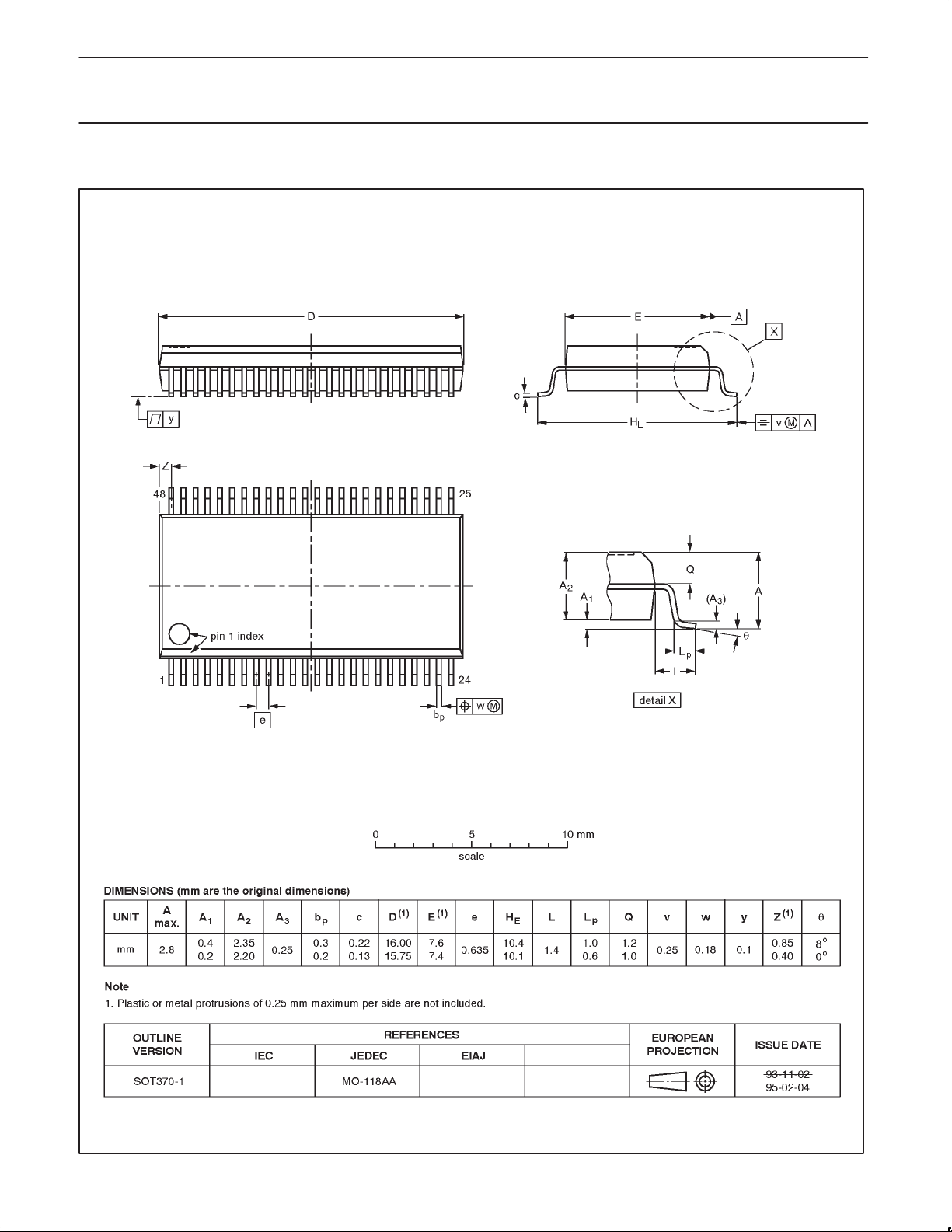
SSOP48: plastic shrink small outline package; 48 leads; body width 7.5 mm SOT370-1
74LVC16245A/
74LVCH16245A
1997 Sep 25
7
Page 8

Philips Semiconductors Product specification
16-bit bus transceiver with direction pin; 5V tolerant
(3-State)
TSSOP48: plastic thin shrink small outline package; 48 leads; body width 6.1mm SOT362-1
74LVC16245A/
74LVCH16245A
1997 Sep 25
8
Page 9

Philips Semiconductors Product specification
16-bit bus transceiver with direction pin; 5V tolerant
(3-State)
NOTES
74LVC16245A/
74LVCH16245A
1997 Sep 25
9
Page 10

Philips Semiconductors Product specification
16-bit bus transceiver with direction pin; 5V tolerant
(3-State)
DEFINITIONS
74LVC16245A/
74LVCH16245A
Data Sheet Identification Product Status Definition
Objective Specification
Preliminary Specification
Product Specification
Philips Semiconductors and Philips Electronics North America Corporation reserve the right to make changes, without notice, in the products,
including circuits, standard cells, and/or software, described or contained herein in order to improve design and/or performance. Philips
Semiconductors assumes no responsibility or liability for the use of any of these products, conveys no license or title under any patent, copyright,
or mask work right to these products, and makes no representations or warranties that these products are free from patent, copyright, or mask
work right infringement, unless otherwise specified. Applications that are described herein for any of these products are for illustrative purposes
only. Philips Semiconductors makes no representation or warranty that such applications will be suitable for the specified use without further testing
or modification.
LIFE SUPPORT APPLICA TIONS
Philips Semiconductors and Philips Electronics North America Corporation Products are not designed for use in life support appliances, devices,
or systems where malfunction of a Philips Semiconductors and Philips Electronics North America Corporation Product can reasonably be expected
to result in a personal injury. Philips Semiconductors and Philips Electronics North America Corporation customers using or selling Philips
Semiconductors and Philips Electronics North America Corporation Products for use in such applications do so at their own risk and agree to fully
indemnify Philips Semiconductors and Philips Electronics North America Corporation for any damages resulting from such improper use or sale.
Philips Semiconductors
811 East Arques Avenue
P.O. Box 3409
Sunnyvale, California 94088–3409
Telephone 800-234-7381
Formative or in Design
Preproduction Product
Full Production
This data sheet contains the design target or goal specifications for product development. Specifications
may change in any manner without notice.
This data sheet contains preliminary data, and supplementary data will be published at a later date. Philips
Semiconductors reserves the right to make changes at any time without notice in order to improve design
and supply the best possible product.
This data sheet contains Final Specifications. Philips Semiconductors reserves the right to make changes
at any time without notice, in order to improve design and supply the best possible product.
Copyright Philips Electronics North America Corporation 1997
print code Date of release: 05-96
Document order number: 9397-750-04531
All rights reserved. Printed in U.S.A.
yyyy mmm dd
10
 Loading...