

Datasheet 74LVC157PW, 74LVC157DB, 74LVC157D, 74LVC157APW, 74LVC157ADB Datasheet (Philips)
...Page 1

74LVC157A
Quad 2-input multiplexer
Product specification
Supercedes data of 1997 Nov 07
IC24 Data Handbook
1998 Jul 29
INTEGRATED CIRCUITS
Page 2
Philips Semiconductors Product specification
74L VC157AQuad 2-input multiplexer
2
1998 Jul 29 853-1945 19802
FEA TURES
•Wide supply voltage range of 1.2 to 3.6 V
•In accordance with JEDEC standard no. 8-1A
•CMOS lower power consumption
•Direct interface with TTL levels
•5 Volt tolerant inputs, for interfacing with 5 Volt logic
DESCRIPTION
The 74LVC157A is a high-performance, low-power, Si-gate CMOS
device, superior to most advanced CMOS compatible TTL families.
Inputs can be driven from either 3.3V or 5.0V devices. In 3-State
operation, outputs can handle 5V. This feature allows the use of
these devices as translators in a mixed 3.3V/5V environment.
The 74LVC157A is a quad 2-input multiplexer which select 4 bits of
data from two sources under the control of a common data select
input (S). The four outputs present the selected data in the true
(non-inverted) form. The enable input (E
) is active LOW. When E is
HIGH, all of the outputs (1Y to 4Y) are forced LOW regardless of all
other input conditions. Moving the data from two groups of registers
to four common output buses is a common use of the 74LV157. The
state of the common data select input (S) determines the particular
register from which the data comes. It can also be used as function
generator.
The device is useful for implementing highly irregular logic by
generating any four of the 16 different functions of two variables with
one variable common.
The 74LVC157A is the logic implementation of a 4-pole, 2-position
switch, where the position of the switch is determined by the logic
levels applied to S.
QUICK REFERENCE DA TA
GND = 0 V; T
amb
= 25°C; tr = t
f
≤ 2.5 ns
SYMBOL
PARAMETER CONDITIONS TYPICAL UNIT
t
PHL/tPLH
Propagation delay
nl0, nl1, to nY
E
to nY
S to nY
CL = 50 pF;
VCC = 3.3 V
3.1
3.0
3.3
ns
C
I
Input capacitance 5.0 pF
C
PD
Power dissipation capacitance per gate VI = GND to V
CC
1
33 pF
NOTES:
1. C
PD
is used to determine the dynamic power dissipation (PD in µW)
P
D
= CPD × V
CC
2
× fi Σ (CL × V
CC
2
× fo) where:
f
i
= input frequency in MHz; CL = output load capacitance in pF;
f
o
= output frequency in MHz; VCC = supply voltage in V;
Σ (C
L
× V
CC
2
× fo) = sum of the outputs.
ORDERING INFORMATION
PACKAGES TEMPERATURE RANGE OUTSIDE NORTH AMERICA NORTH AMERICA PKG. DWG. #
16-Pin Plastic SO –40°C to +85°C 74LVC157A D 74LVC157A D SOT109-1
16-Pin Plastic SSOP Type II –40°C to +85°C 74LVC157A DB 74LVC157A DB SOT338-1
16-Pin Plastic TSSOP Type I –40°C to +85°C 74LVC157A PW 74LVC157APW DH SOT403-1
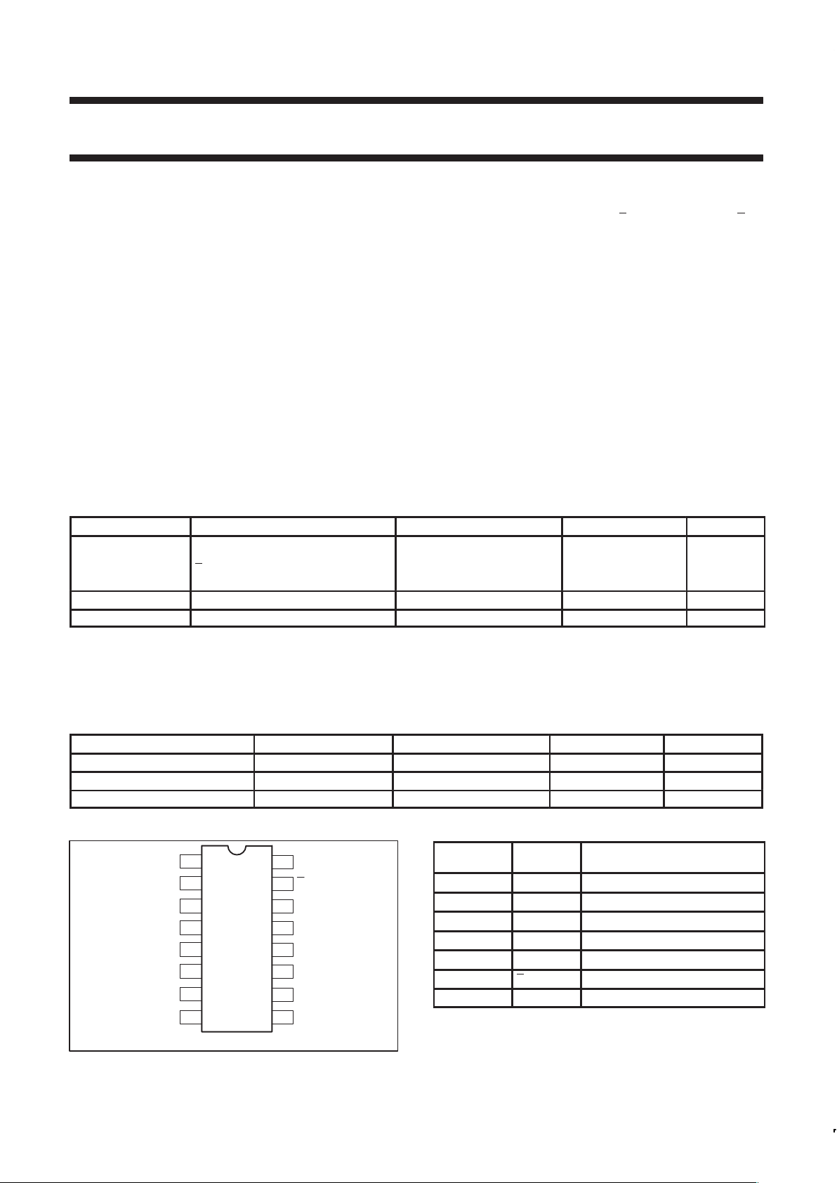
PIN CONFIGURATION
SV00563
1
2
3
4
5
6
S
1I
0
1I
1
1Y
2I
0
2I
1
V
CC
E
4I
0
4I
1
4Y
3I
0
16
15
14
13
12
11
7
8
2Y
GND
3I
1
3Y
10
9
PIN DESCRIPTION
PIN
NUMBER
SYMBOL FUNCTION
1 S Common data select input
2, 5, 11, 14 1l0 to 4l
0
Data inputs from sources 0
3, 6, 10, 13 1l1 to 4l
1
Data inputs from sources 1
4, 7, 9, 12 1Y to 4Y Multiplexer outputs
8 GND Ground (0 V)
15 E Enable input (active LOW)
16 V
CC
Positive supply voltage
Page 3

Philips Semiconductors Product specification
74LVC157AQuad 2-input multiplexer
1998 Jul 29
3
LOGIC SYMBOL
SV00564
1
S
E
2
1I
0
2I
0
3I
0
4I
0
1I
1
2I
1
3I
1
4I
1
35
4
1Y
6
7
2Y
10
12
4Y
1411
9
3Y
13
15
LOGIC SYMBOL (IEEE/IEC)
SV00565
EN
G1
15
1
7
4
9
12
6
5
3
2
MUX
1
11
10
14
13
1
FUNCTIONAL DIAGRAM
SV00566
E
S
SELECTOR
MULTIPLEXER
OUTPUTS
1I
0
1Y
2Y
3Y
4Y
1I
1
2I
0
2I
1
3I
0
3I
1
4I
0
4I
1
115
7
4
9
12
6
5
2
3
11
10
14
13
FUNCTION T ABLE
INPUTS OUTPUTS
E S nl
0
nl
1
nY
H X X X L
L L L X L
L L H X H
L H X L L
L H X H H
NOTES:
H = HIGH voltage level
L = LOW voltage level
X = don’t care
LOGIC DIAGRAM
SV00581
S
1Y
2Y
3Y
4Y
1I
1
1I
0
2I
1
2I
0
3I
1
3I
0
4I
1
4I
0
E
Page 4

Philips Semiconductors Product specification
74LVC157AQuad 2-input multiplexer
1998 Jul 29
4
RECOMMENDED OPERATING CONDITIONS
LIMITS
SYMBOL
PARAMETER
CONDITIONS
MIN MAX
UNIT
DC supply voltage (for max. speed performance) 2.7 3.6
V
CC
DC supply voltage (for low-voltage applications) 1.2 3.6
V
V
I
DC input voltage range 0 5.5 V
V
O
DC output voltage range 0 V
CC
V
T
amb
Operating free-air temperature range –40 +85 °C
tr, t
f
Input rise and fall times
VCC = 1.2 to 2.7V
VCC = 2.7 to 3.6V
0
0
20
10
ns/V
ABSOLUTE MAXIMUM RATINGS
1
In accordance with the Absolute Maximum Rating System (IEC 134).
Voltages are referenced to GND (ground = 0V).
SYMBOL
PARAMETER CONDITIONS RATING UNIT
V
CC
DC supply voltage –0.5 to +6.5 V
I
IK
DC input diode current VIt 0 –50 mA
V
I
DC input voltage Note 2 –0.5 to +5.5 V
I
OK
DC output diode current V
O
uVCC or VO t 0 "50 mA
V
O
DC output voltage Note 2 –0.5 to VCC +0.5 V
I
O
DC output diode current VO = 0 to V
CC
"50 mA
I
GND
, I
CC
DC VCC or GND current "100 mA
T
stg
Storage temperature range –65 to +150 °C
Power dissipation per package
P
TOT
– plastic mini-pack (SO) above +70°C derate linearly with 8 mW/K 500
– plastic shrink mini-pack (SSOP and TSSOP) above +60°C derate linearly with 5.5 mW/K 500
mW
NOTES:
1. Stresses beyond those listed may cause permanent damage to the device. These are stress ratings only and functional operation of the
device at these or any other conditions beyond those indicated under “recommended operating conditions” is not implied. Exposure to
absolute-maximum-rated conditions for extended periods may affect device reliability .
2. The input and output voltage ratings may be exceeded if the input and output current ratings are observed.
Page 5

Philips Semiconductors Product specification
74LVC157AQuad 2-input multiplexer
1998 Jul 29
5
DC ELECTRICAL CHARACTERISTICS
Over recommended operating conditions. V oltages are referenced to GND (ground = 0V).
LIMITS
SYMBOL PARAMETER TEST CONDITIONS Temp = -40°C to +85°C UNIT
MIN TYP1MAX
p
VCC = 1.2V V
CC
VIHHIGH level Input voltage
VCC = 2.7 to 3.6V 2.0
V
p
VCC = 1.2V GND
VILLOW level Input voltage
VCC = 2.7 to 3.6V 0.8
V
VCC = 2.7V; VI = VIH or VIL; IO = –12mA VCC*0.5
p
VCC = 3.0V; VI = VIH or VIL; IO = –100µA VCC*0.2 V
CC
VOHHIGH level output voltage
VCC = 3.0V; VI = VIH or V
IL;
IO = –18mA VCC*0.6
V
VCC = 3.0V; VI = VIH or V
IL;
IO = –24mA VCC*0.8
VCC = 2.7V; VI = VIH or VIL; IO = 12mA 0.40
V
OL
LOW level output voltage
VCC = 3.0V; VI = VIH or VIL; IO = 100µA GND 0.20
V
VCC = 3.0V; VI = VIH or V
IL;
IO = 24mA 0.55
p
;
IIInput leakage current
V
CC
= 3.6V;
V
I
= 5.5V or
GND
"0.1
"5µA
I
CC
Quiescent supply current VCC = 3.6V; VI = VCC or GND; IO = 0 0.1 10 µA
∆I
CC
Additional quiescent supply current per
input pin
VCC = 2.7V to 3.6V; VI = VCC –0.6V; IO = 0 5 500 µA
NOTE:
1. All typical values are measured at V
CC
= 3.3V and T
amb
= 25°C.
AC CHARACTERISTICS
GND = 0 V; tr = tf v 2.5 ns; CL = 50 pF; RL = 500; T
amb
= –40C to +85C
LIMITS
SYMBOL PARAMETER WAVEFORM VCC = 3.3V ±0.3V VCC = 2.7V VCC = 1.2V UNIT
MIN TYP1MAX MIN MAX TYP
t
PHL/tPLH
Propagation delay
nl0 to nY;
nl1 to nY
Figure 2, 3 1.5 3.1 5.7 1.5 6.7 12 ns
t
PHL/tPLH
Propagation delay
E to nY
Figure 1, 3 1.5 3.0 6.3 1.5 7.3 11 ns
t
PHL/tPLH
Propagation delay
S to nY
Figure 2, 3 1.5 3.3 6.8 1.5 7.8 13 ns
NOTE:
1. These typical values are at V
CC
= 3.3V and T
amb
= 25°C.
Page 6

Philips Semiconductors Product specification
74LVC157AQuad 2-input multiplexer
1998 Jul 29
6
AC WAVEFORMS
VM = 0.5 × V
CC
at VCC < 2.7 V
V
M
= 1.5 V at VCC ≥ 2.7 V
V
X
= VOL + 0.3 V at VCC ≥ 2.7 V
V
X
= VOL + 0.1 ×V
CC
at V
CC
< 2.7 V
V
Y
= VOH – 0.3 V at VCC ≥ 2.7V
V
Y
= VOH – 0.1 × VCC at VCC < 2.7 V
V
OL
and VOH are the typical output voltage drop that occur with the
output load.
SV00561
V
M
E
INPUT
nY OUTPUTS
V
M
t
PLH
t
PHL
GND
V
I
V
OL
V
OH
Figure 1. Enable input (E) to output (nY) propagation delays.
SV00562
V
M
nI
0
, nI1, S
INPUTS
nY OUTPUT
V
M
t
PLH
t
PHL
GND
V
I
V
OL
V
OH
Figure 2. Data inputs (nI0, nI1) and common data select
input (S) to output (nY) propagation delays.
TEST CIRCUIT
SWITCH POSITION
PULSE
GENERATOR
R
T
V
I
D.U.T.
V
O
C
L
V
CC
500Ω
Open
GND
S
1
V
CC
V
I
< 2.7V V
CC
TEST S
1
t
PLH/tPHL
Open
2.7V2.7–3.6V
50pF
500Ω
2 * V
CC
SV00903
Figure 3. Load circuitry for switching times.
Page 7

Philips Semiconductors Product specification
74LVC157AQuad 2-input multiplexer
1998 Jul 29
7
SO16: plastic small outline package; 16 leads; body width 3.9 mm SOT109-1
Page 8

Philips Semiconductors Product specification
74LVC157AQuad 2-input multiplexer
1998 Jul 29
8
SSOP16: plastic shrink small outline package; 16 leads; body width 5.3 mm SOT338-1
Page 9

Philips Semiconductors Product specification
74LVC157AQuad 2-input multiplexer
1998 Jul 29
9
TSSOP16: plastic thin shrink small outline package; 16 leads; body width 4.4 mm SOT403-1
Page 10

Philips Semiconductors Product specification
74LVC157AQuad 2-input multiplexer
yyyy mmm dd
10
Definitions
Short-form specification — The data in a short-form specification is extracted from a full data sheet with the same type number and title. For
detailed information see the relevant data sheet or data handbook.
Limiting values definition — Limiting values given are in accordance with the Absolute Maximum Rating System (IEC 134). Stress above one
or more of the limiting values may cause permanent damage to the device. These are stress ratings only and operation of the device at these or
at any other conditions above those given in the Characteristics sections of the specification is not implied. Exposure to limiting values for extended
periods may affect device reliability.
Application information — Applications that are described herein for any of these products are for illustrative purposes only. Philips
Semiconductors make no representation or warranty that such applications will be suitable for the specified use without further testing or
modification.
Disclaimers
Life support — These products are not designed for use in life support appliances, devices or systems where malfunction of these products can
reasonably be expected to result in personal injury . Philips Semiconductors customers using or selling these products for use in such applications
do so at their own risk and agree to fully indemnify Philips Semiconductors for any damages resulting from such application.
Right to make changes — Philips Semiconductors reserves the right to make changes, without notice, in the products, including circuits, standard
cells, and/or software, described or contained herein in order to improve design and/or performance. Philips Semiconductors assumes no
responsibility or liability for the use of any of these products, conveys no license or title under any patent, copyright, or mask work right to these
products, and makes no representations or warranties that these products are free from patent, copyright, or mask work right infringement, unless
otherwise specified.
Philips Semiconductors
811 East Arques Avenue
P.O. Box 3409
Sunnyvale, California 94088–3409
Telephone 800-234-7381
Copyright Philips Electronics North America Corporation 1998
All rights reserved. Printed in U.S.A.
print code Date of release: 08-98
Document order number: 9297-750-04495
Data sheet
status
Objective
specification
Preliminary
specification
Product
specification
Product
status
Development
Qualification
Production
Definition
[1]
This data sheet contains the design target or goal specifications for product development.
Specification may change in any manner without notice.
This data sheet contains preliminary data, and supplementary data will be published at a later date.
Philips Semiconductors reserves the right to make chages at any time without notice in order to
improve design and supply the best possible product.
This data sheet contains final specifications. Philips Semiconductors reserves the right to make
changes at any time without notice in order to improve design and supply the best possible product.
Data sheet status
[1] Please consult the most recently issued datasheet before initiating or completing a design.
 Loading...