

Page 1
LOW VOLTAGE CMOS QUAD BUS BUFFERS (3-STATE)
■ 5V TOLERANT INPUTS
■ HIGH SPEED:t
■ POWER DOWN PROTECTION ON INPUTS
AND OUTPUTS
■ SYMMETRICAL OUTPUT IMPEDANCE:
|I
|=IOL= 24mA (MIN) at VCC=3V
OH
■ PCI BUS LEVELS GUARANTEEDAT 24 mA
■ BALANCED PROPAGATION DELAYS:
t
≅ t
PLH
PHL
■ OPERATING VOLTAGE RANGE:
V
(OPR) = 1.65V to 3.6V (1.2V Data
CC
Retention)
■ PIN AND FUNCTION COMPATIBLE WITH
74 SERIES 125
■ LATCH-UP PERFORMANCE EXCEEDS
500mA (JESD 17)
■ ESD PERFORMANCE:
HBM > 2000V (MIL STD 883 method 3015);
MM > 200V
DESCRIPTION
The 74LVC125A is a low voltage CMOS QUAD
BUS BUFFER fabricated with sub-micron silicon
gate and double-layer metal wiring C
technology. I t is ideal for 1.65 to 3.6 V
operations and low power and low noise
applications.
= 4. 8ns (MAX.) at VCC=3V
PD
2
MOS
CC
74LVC125A
HIGH PERFORMANCE
TSSOPSOP
ORDER CODES
PACKAGE TUBE T & R
SOP 74LVC125AM 74LVC125AMTR
TSSOP 74LVC125ATTR
It can be interfaced to 5V signal environment for
inputs in mixed 3.3/5V system.
These devices require the sam e 3-STATE control
input G
to the high impedance state.
It has more speed performance at 3.3V than 5V
AC/ACT family, combined with a lower power
consumption.
All inputs and outputs are e quipped with
protection circuits against static discharge, giving
them 2KV ESD immunity and transient excess
voltage.
to be taken high to make the output go in
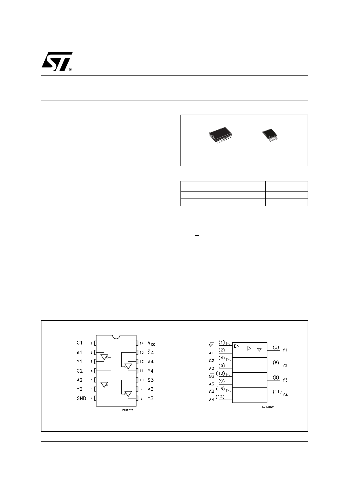
PIN CONNECTION AND IEC LOGIC SYMBOLS
1/9December 2002
Page 2
74LVC125A
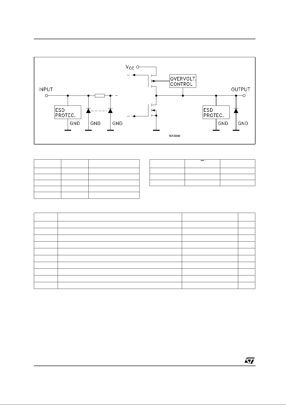
INPUT AND O UTPUT EQUIVALENT CIRCUIT
PIN DESCRIPTION TRUTH TABLE
PIN No SYMBOL NAME AND FUNCTION
1, 4, 9, 12 G1 to G4 Output Enable Inputs
2, 5, 10, 13 A1 to A4 Data Inputs
3, 6, 8, 11 Y1 to Y4 Data Outputs
7 GND Ground (0V)
14
V
CC
Positive Supply Voltage
X : Don’tcare
Z : High Impedance
AGY
XHZ
LLL
HLH
ABSOLUTE MAXIMUM RATINGS
Symbol Parameter Value Unit
V
V
V
V
I
I
OK
I
or I
I
CC
T
T
Absolute Maximum Ratings are those values beyond which damage to the device may occur. Functional operation under these conditions is
not implied
absolute maximum rating must be observed
1) I
O
2) VO<GND
Supply Voltage
CC
DC Input Voltage
I
DC Output Voltage (High Impedance or VCC=0V)
O
DC Output Voltage (High or Low State) (note 1) -0.5 to VCC+ 0.5
O
DC Input Diode Current
IK
DC Output Diode Current (note 2)
DC Output Current
O
DC VCCor Ground Current per Supply Pin
GND
Storage Temperature
stg
Lead Temperature (10 sec)
L
-0.5 to +7.0 V
-0.5 to +7.0 V
-0.5 to +7.0 V
V
-50 mA
-50 mA
± 50 mA
± 100 mA
-65 to +150 °C
300 °C
2/9
Page 3
74LVC125A
RECOMMENDED OPERATING CONDITIONS
Symbol Parameter Value Unit
V
V
V
V
I
OH,IOL
I
OH,IOL
I
OH,IOL
I
OH,IOL
T
dt/dv Input Rise and Fall Time (note 2) 0 to 10 ns/V
1) Truth Table guaranteed: 1.2V to 3.6V
2) V
from0.8V to2Vat VCC=3.0V
IN
DC SPECIFICATIONS
Supply Voltage (note 1)
CC
Input Voltage
I
Output Voltage (High Impedance or VCC= 0V)
O
Output Voltage (High or Low State) 0 to V
O
High or Low Level Output Current (VCC= 3.0 to 3.6V)
High or Low Level Output Current (VCC= 2.7 to 3.0V)
High or Low Level Output Current (VCC= 2.3 to 2.7V)
High or Low Level Output Current (VCC= 1.65 to 2.3V)
Operating Temperature
op
Test Condition Value
1.65 to 3.6 V
0 to 5.5 V
0 to 5.5 V
CC
± 24 mA
± 12 mA
± 8mA
± 4mA
-55 to 125 °C
V
Symbol Parameter
V
V
V
V
I
off
I
OZ
High Level Input
IH
Voltage
Low Level Input
IL
Voltage
High Level Output
OH
Voltage
Low Level Output
OL
Voltage
Input Leakage
I
I
Current
Power Off Leakage
Current
High Impedance
Output Leakage
Current
I
CC
∆I
Quiescent Supply
Current
ICCincr. per Input
CC
V
CC
(V)
1.65 to 1.95
-40 to 85 °C -55 to 125 °C
Min. Max. Min. Max.
0.65V
CC
0.65V
CC
2.3to2.7 1.7 1.7
2.7to3.6 2 2
1.65 to 1.95
0.35V
CC
0.35V
2.3 to 2.7 0.7 0.7
2.7 to 3.6 0.8 0.8
1.65 to 3.6
1.65
2.3
2.7
3.0
3.0
1.65 to 3.6
1.65
2.3
2.7
3.0
3.6
0
3.6 VI=VIHorV
IO=-100 µAVCC-0.2 VCC-0.2
=-4 mA
I
O
=-8 mA
I
O
=-12 mA
I
O
=-18 mA
I
O
=-24 mA
I
O
IO=100 µA
=4 mA
I
O
=8 mA
I
O
=12 mA
I
O
I
=24 mA
O
= 0 to 5.5V
V
I
or VO= 5.5V
V
I
IL
1.2 1.2
1.7 1.7
2.2 2.2
2.4 2.4
2.2 2.2
0.2 0.2
0.45 0.45
0.7 0.7
0.4 0.4
0.55 0.55
± 5 ± 5 µA
10 10 µA
±5 ±5 µA
VO=0to5.5V
3.6
2.7to3.6
VI=VCCor GND
or VO= 3.6 to
V
I
5.5V
VIH=VCC-0.6V
10 10
± 10 ± 10
500 500 µA
Unit
V
CC
V
V
V
µA
3/9
Page 4

74LVC125A
DYNAMIC SWITCHING CHARACTERISTICS
Test Condition Value
=25°C
Symbol Parameter
V
CC
(V)
V
OLP
V
OLV
1) Number of output defined as "n". Measured with "n-1" outputs switching from HIGH to LOW or LOW to HIGH. The remaining output is
measured in the LOW state.
Dynamic Low Level Quiet
Output (note 1)
3.3
=50pF
C
L
V
=0V,VIH= 3.3V
IL
AC ELECTRICAL CHARACTERISTICS
Test Condition Value
T
A
Min. Typ. Max.
0.8
-0.8
Unit
V
Symbol Parameter
t
PLHtPHL
Propagation Delay
Time
V
(V)
CC
C
(pF)
R
(Ω)
t
L
s
(ns)
L
1.65 to 1.95 30 1000 2.0 9.0 12
2.3 to 2.7 30 500 2.0 6.3 8.5
2.7 50 500 2.5 1.5 5.5 6.5
-40 to 85 °C -55 to 125 °C
= t
r
Min. Max. Min. Max.
Unit
ns
3.0 to 3.6 50 500 2.5 1 4.8 5.8
t
PZLtPZH
Output Enable Time 1.65 to 1.95 30 1000 2.0 9.9 13
2.3 to 2.7 30 500 2.0 7.4 9.6
2.7 50 500 2.5 1 6.6 7.9
ns
3.0 to 3.6 50 500 2.5 1 5.4 6.5
t
PLZtPHZ
Output Disable Time 1.65 to 1.95 30 1000 2.0 11 14
2.3 to 2.7 30 500 2.0 5.6 7.3
2.7 50 500 2.5 2 5.0 6.0
ns
3.0 to 3.6 50 500 2.5 2 4.6 5.5
t
OSLH
t
OSHL
1) Skew is defined as theabsolutevalue ofthe difference between the actual propagation delay for any two outputs of the samedevice switching in the same direction, either HIGH or LOW (t
2) Parameter guaranteed by design
Output To Output
Skew Time (note1,
2)
2.7to3.6 1 1 ns
OSLH
=|t
PLHm-tPLHn
|, t
OSHL
=|t
PHLm-tPHLn
|
CAPACITIVE CHARACTERISTICS
Test Condition Value
=25°C
Symbol Parameter
C
C
Input Capacitance
IN
Power Dissipation Capacitance
PD
(note 1)
V
CC
(V)
1.8 fIN= 10MHz 28
T
A
Min. Typ. Max.
4pF
Unit
pF2.5 30
3.3 34
1) CPDis defined as the value of the IC’s internal equivalent capacitance which is calculated from the operating current consumption without
load. (Refer to Test Circuit). Average operating current can be obtained by the following equation. I
CC(opr)=CPDxVCCxfIN+ICC
/n(percircuit)
4/9
Page 5

TEST CIRCUIT
74LVC125A
RT=Z
of pulse generator (typically 50Ω)
OUT
TEST CIRCUIT AND WAV EFOR M SYMBOL VALUE
Symbol
C
L
R
L=R1
V
S
V
IH
V
M
V
OH
V
X
V
Y
t
r=tr
1.65 to 1.95V 2.3 to 2.7V 2.7V 3.0 to 3.6V
30pF 30pF 50pF 50pF
1000Ω 500Ω 500Ω 500Ω
2xV
V
CC
CC
2xV
V
CC
VCC/2 VCC/2 1.5V 1.5V
V
CC
V
CC
VOL+ 0.15V VOL+ 0.15V VOL+ 0.3V VOL+ 0.3V
VOH- 0.15V VOH- 0.15V VOH- 0.3V VOH- 0.3V
<2.0ns <2.0ns <2.5ns <2.5ns
CC
V
CC
6V 6V
2.7V 2.7V
3.0V 3.0V
5/9
Page 6

74LVC125A
WAVEFORM 1: PROPAGATION DELAYS (f=1MHz; 50% duty cycle)
WAVEFORM 2: OUTPUT ENABLE AND DISABLE TIME (f=1MHz; 50% duty cycle)
6/9
Page 7

SO-14 MECHANICAL DATA
74LVC125A
DIM.
A 1.75 0.068
a1 0.1 0.2 0.003 0.007
a2 1.65 0.064
b 0.35 0.46 0.013 0.018
b1 0.19 0.25 0.007 0.010
C 0.5 0.019
c1 45˚ (typ.)
D 8.55 8.75 0.336 0.344
E 5.8 6.2 0. 228 0.244
e 1.27 0.050
e3 7.62 0.300
F 3.8 4.0 0.149 0.157
G 4.6 5.3 0.181 0.208
L 0.5 1.27 0.019 0.050
M 0.68 0.026
S ˚ (max.)
MIN. TYP MAX. MIN. TYP. MAX.
mm. inch
8
PO13G
7/9
Page 8

74LVC125A
TSSOP14 MECHANICAL DATA
mm. inch
DIM.
MIN. TYP MAX. MIN. TYP. MAX.
A 1.2 0.047
A1 0.05 0.15 0.002 0.004 0.006
A2 0.8 1 1.05 0.031 0.039 0.041
b 0.19 0.30 0.007 0.012
c 0.09 0.20 0.004 0.0089
D 4.9 5 5.1 0.193 0.197 0.201
E 6.2 6.4 6.6 0.244 0.252 0.260
E1 4.3 4.4 4.48 0.169 0.173 0.176
e 0.65 BSC 0.0256 BSC
K0˚ 8˚0˚ 8˚
L 0.45 0.60 0.75 0.018 0.024 0.030
A2
A
A1
b
e
c
K
L
E
D
E1
PIN 1 IDENTIFICATION
8/9
1
0080337D
Page 9

74LVC125A
Information furnished is believed to be accurate and reliable. However, STMicroelectronics assumes no responsibility f or the
consequences of use of such informatio n nor for any infringement of paten ts or o ther rig hts of t hird part ies which ma y result from
its use. No license is granted by implication or otherwise under any patent or patent rights of STMicroelectronics. Specifications
mentioned in this publication are subject to change without notice. This publication supersedes and replaces all information
previousl y suppl ied. STM icroel ectronics produc ts are not auth orized for use as c ritica l compone nts in l ife s upport dev ices or
systems without express written approval of STMicroelectronics.
Australia - Brazil - Canada - China - Finland - France - Germany - Hong Kong - India - Israel - Italy - Japan - Malaysia - Malta - Morocco
© The ST logo is a registered trademark of STMicroelectronics
© 2002 STMicroelectronics - Printed in Italy - All Rights Reserved
STMicroelectronics GROUP OF COMPANIES
Singapore - Spain - Sweden - Switzerland - United Kingdom - United States.
© http://www.st.com
9/9
 Loading...