

Page 1
74LV4094
8-stage shift-and-store bus register
Product specification 1998 Jun 23
INTEGRATED CIRCUITS
Page 2
Philips Semiconductors Product specification
74L V40948-stage shift-and-store bus register
2
1998 Jun 23 853-2078 19619
FEA TURES
•Optimized for low voltage applications: 1.0 to 3.6 V
•Accepts TTL input levels between V
CC
= 2.7 V and V
CC
= 3.6 V
•Typical V
OLP
(output ground bounce) < 0.8 V at V
CC
= 3.3 V ,
T
amb
= 25°C
•Typical V
OHV
(output VOH undershoot) > 2 V at V
CC
= 3.3 V ,
T
amb
= 25°C
•Output capability: standard
•I
CC
category: MSI
Applications:
•Serial-to-parallel data conversion
•Remote control holding register
DESCRIPTION
The 74LV4094 is a low-voltage Si-gate CMOS device and is pin and
function compatible with 74HC/HCT4094.
The 74LV4094 is an 8-stage serial shift register having a storage
latch associated with each stage for strobing data from the serial
input (D) to the parallel buffered 3-State outputs (QP
0
to OP7). The
parallel outputs may be connected directly to the common bus lines.
Data is shifted on the positive-going clock (CP) transitions. The data
in each shift register is transferred to the storage register when the
strobe input (STR) is HIGH. Data in the storage register appears at
the outputs whenever the output enable input (OE) signal is HIGH.
Two serial outputs (QS
1
and QS2) are available for cascading a
number of 74LV4094 devices. Data is available at QS
1
on the
positive-going clock edges to allow high-speed operation in
cascaded systems in which the clock rise time is fast. The same
serial information is available at QS
2
on the next negative going
clock edge and is for cascading 74LV4094 devices when the clock
rise time is slow.
QUICK REFERENCE DA TA
GND = 0 V; T
amb
= 25°C; tr =t
f
≤ 2.5 ns
SYMBOL
PARAMETER CONDITIONS TYPICAL UNIT
t
PHL/tPLH
Propagation delay
CP to QS
1
CP to QS
2
CP to QP
n
STR to QP
n
CL = 15 pF;
VCC = 3.3 V
14
13
18
17
ns
f
MAX
Maximum clock frequency
95
MHz
C
I
Input capacitance 3.5 pF
C
PD
Power dissipation capacitance per gate
VCC = 3.3 V
VI = GND to V
CC
NO TAG
83 pF
NOTE:
1. C
PD
is used to determine the dynamic power dissipation (PD in µW)
P
D
= CPD × V
CC
2
× fi (CL × V
CC
2
× fo) where:
f
i
= input frequency in MHz; CL = output load capacity in pF;
f
o
= output frequency in MHz; VCC = supply voltage in V;
(C
L
× V
CC
2
× fo) = sum of the outputs.
ORDERING INFORMATION
PACKAGES TEMPERATURE RANGE OUTSIDE NORTH AMERICA NORTH AMERICA PKG. DWG. #
16-Pin Plastic DIL –40°C to +125°C 74LV4094 N 74LV4094 N SOT38-4
16-Pin Plastic SO –40°C to +125°C 74LV4094 D 74LV4094 D SOT109-1
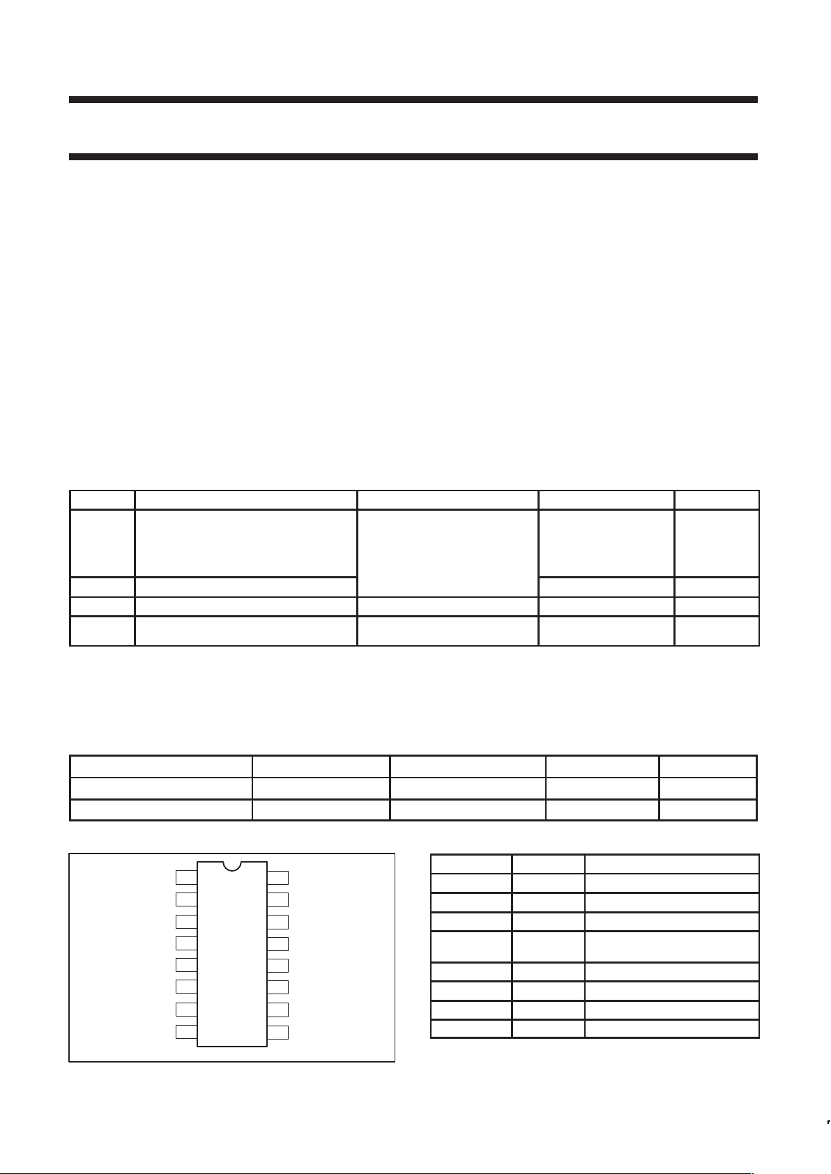
PIN CONFIGURATION
SV01611
1
2
3
4
5
6
STR
D
CP
QP
0
QP
1
QP
2
V
CC
OE
QP
4
16
15
14
13
12
11
7
8
GND
QS
2
QS
1
10
9
QP
3
QP
5
QP
6
QP
7
PIN DESCRIPTION
PIN NUMBER SYMBOL FUNCTION
1 STR Strobe input
2 D Serial input
3 CP Clock input
4, 5, 6, 7, 14,
13, 12, 11
QP0 to QP7Parallel outputs
8 GND Ground (0 V)
9, 10 QS1, QS
2
Serial outputs
15 OE Output enable input
16 V
CC
Positive supply voltage
Page 3
Philips Semiconductors Product specification
74LV40948-stage shift-and-store bus register
1998 Jun 23
3
LOGIC SYMBOL
SV01612
1
2
3
4
5
6
STR
D
CP
QP
0
QP
1
QP
2
OE
QP
4
QP
5
QP
6
QP
7
15
14
13
12
11
7
QP
3
QS
2
QS
1
10
9
FUNCTIONAL DIAGRAM
3-STATE OUTPUTS
8-STATE SHIFT
REGISTER
8-BIT STORAGE
REGISTER
SV01614
2
3
1
15
D
CP
STR
OE
QS
2
QS
1
QP0QP1QP2QP3QP4Q51QP6QP
7
9
10
4 5 6 7 14 13 12 11
LOGIC SYMBOL (IEEE/IEC)
SV01613
4
5
6
7
14
13
12
11
9
10
2D
3
1D
C2
EN3
1
15
3
2
SRG8
C1/
LOGIC DIAGRAM
SV01615
DCPQ
latch
D
CP
D
CP
D
CP
D
CP
D
CP
Q
Q
Q
Q
Q
FF0 FF7
latch latch
STAGE 0 STAGE 7
STAGES 1 TO 6
D
CP
STR
OE
QP0QP
1
QP
2
QP
3
QP
4
QP
5
QP
6
QP
7
Q
7
’
QS
2
Page 4
Philips Semiconductors Product specification
74LV40948-stage shift-and-store bus register
1998 Jun 23
4
FUNCTION TABLE
INPUTS PARALLEL OUTPUT SERIAL OUTPUTS
CP OE STR D QP
0
QP
n
QS
1
QS
2
↑ L X X Z Z Q’
6
NC
↓ L X X Z Z NC QP
7
↑ H L X NC NC Q’
6
NC
↑ H H L L QP
n–1
Q’
6
NC
↑ H H H H QP
n–1
Q’
6
NC
↓ H H H NC NC NC QP
7
NOTES:
H = HIGH voltage level
L = LOW voltage level
X = don’t care
Z = high impedance OFF-state
NC = no change
↑ = LOW-to–HIGH CP transition
↓ = HIGH-to-LOW CP transition
Q’
6
= the information in the 8th register stage is transferred to the
8
th
register stage and QSn clock edge.
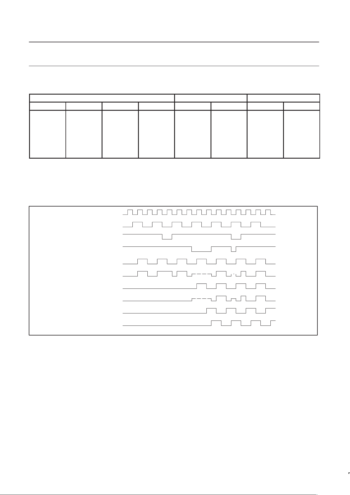
TIMING DIAGRAM
SV01616
CPCLOCK INPUT
DATA INPUT
STROBE INPUT
OUTPUT ENABLE INPUT
INTERNAL Q’0 (FF0)
OUTPUT
INTERNAL Q’6 (FF6)
OUTPUT
Z–state
Z–state
SERIAL OUTPUT
SERIAL OUTPUT
D
STR
OE
QP
0
QP
6
QS
2
QS
1
Page 5
Philips Semiconductors Product specification
74LV40948-stage shift-and-store bus register
1998 Jun 23
5
ABSOLUTE MAXIMUM RATINGS
NO TAG, NO TAG
In accordance with the Absolute Maximum Rating System (IEC 134).
Voltages are referenced to GND (ground = 0 V).
SYMBOL
PARAMETER CONDITIONS RATING UNIT
V
CC
DC supply voltage –0.5 to +7.0 V
I
IK
DC input diode current VI < –0.5 or VI > VCC + 0.5V 20 mA
I
OK
DC output diode current VO < –0.5 or VO > VCC + 0.5V 50 mA
I
O
DC output source or sink current
– standard outputs
–0.5V < VO < VCC + 0.5V
25
mA
I
GND
,
I
CC
DC VCC or GND current for types with
– standard outputs 50
mA
T
stg
Storage temperature range –65 to +150 °C
P
TOT
Power dissipation per package
– plastic DIL
– plastic mini-pack (SO)
– plastic shrink mini-pack (SSOP and TSSOP)
for temperature range: –40 to +125°C
above +70°C derate linearly with 12 mW/K
above +70°C derate linearly with 8 mW/K
above +60°C derate linearly with 5.5 mW/K
750
500
400
mW
NOTES:
1. Stresses beyond those listed may cause permanent damage to the device. These are stress ratings only and functional operation of the
device at these or any other conditions beyond those indicated under “recommended operating conditions” is not implied. Exposure to
absolute-maximum-rated conditions for extended periods may affect device reliability .
2. The input and output voltage ratings may be exceeded if the input and output current ratings are observed.
RECOMMENDED OPERATING CONDITIONS
SYMBOL PARAMETER CONDITIONS MIN TYP MAX UNIT
V
CC
DC supply voltage See Note NO TAG 1.0 3.3 3.6 V
V
I
Input voltage 0 – V
CC
V
V
O
Output voltage 0 – V
CC
V
T
amb
Operating ambient temperature range in free air
See DC and AC
characteristics
–40
–40
+85
+125
°C
tr, t
f
Input rise and fall times except for
Schmitt-trigger inputs
VCC = 1.0V to 2.0V
VCC = 2.0V to 2.7V
VCC = 2.7V to 3.6V
–
–
–
–
–
–
500
200
100
ns/V
NOTE:
1. The LV is guaranteed to function down to V
CC
= 1.0V (input levels GND or VCC); DC characteristics are guaranteed from VCC = 1.2V to VCC = 5.5V.
Page 6

Philips Semiconductors Product specification
74LV40948-stage shift-and-store bus register
1998 Jun 23
6
DC ELECTRICAL CHARACTERISTICS
Over recommended operating conditions, voltages are referenced to GND (ground = 0 V)
LIMITS
-40°C to +85°C -40°C to +125°C
SYMBOL
PARAMETER
TEST CONDITIONS
MIN
TYP
NO TAG
MAX MIN MAX
UNIT
VCC = 1.2 V V
CC
0.6 V
CC
V
IH
HIGH l
evel Inpu
t
VCC = 2.0 V 1.4 1.4
V
voltage
VCC = 2.7 to 3.6 V 2.0 2.0
VCC = 1.2 V 0.4 GND GND
V
IL
LOW l
evel Inpu
t
VCC = 2.0 V 0.6 0.6
V
voltage
VCC = 2.7 to 3.6 V 0.8 0.8
VCC = 1.2 V; VI = VIH or V
IL;
–IO = 100µA 1.2
HIGH level output
VCC = 2.0 V; VI = VIH or V
IL;
–IO = 100µA 1.8 2.0 1.8
V
OH
voltage; all outputs
VCC = 2.7 V; VI = VIH or V
IL;
–IO = 100µA 2.5 2.7 2.5
V
VCC = 3.0 V; VI = VIH or V
IL;
–IO = 100µA 2.8 3.0 2.8
V
OH
HIGH level output
voltage;
STANDARD
outputs
VCC = 3.0 V; VI = VIH or V
IL;
–IO = 6mA 2.40 2.82 2.20 V
VCC = 1.2 V; VI = VIH or V
IL;
IO = 100µA 0
LOW level output
VCC = 2.0 V; VI = VIH or V
IL;
IO = 100µA 0 0.2 0.2
V
OL
voltage; all outputs
VCC = 2.7 V; VI = VIH or V
IL;
IO = 100µA 0 0.2 0.2
V
VCC = 3.0 V; VI = VIH or V
IL;
IO = 100µA 0 0.2 0.2
V
OL
LOW level output
voltage;
STANDARD
outputs
VCC = 3.0 V; VI = VIH or V
IL;
IO = 6mA 0.25 0.40 0.50 V
I
I
Input leakage
current
VCC = 3.6 V; VI = VCC or GND 1.0 1.0 µA
I
OZ
3-State output
OFF-state current
VCC = 3.6 V; VI = VIH or V
IL;
VO = VCC or GND
5 10 µA
I
CC
Quiescent supply
current; SSI
VCC = 3.6; VI = VCC or GND; IO = 0 20.0 40 µA
Quiescent supply
current; flip-flops
VCC = 3.6; VI = VCC or GND; IO = 0 20.0 80 µA
I
CC
Quiescent supply
current; MSI
VCC = 3.6 V; VI = VCC or GND; IO = 0 20.0 160
Quiescent supply
current; LSI
VCC = 3.6 V; VI = VCC or GND; IO = 0 500 1000
µA
∆I
CC
Additional
quiescent supply
current per input
VCC = 2.7 V to 3.6 V; VI = VCC – 0.6 V 500 850 µA
NOTE:
1. All typical values are measured at T
amb
= 25°C.
Page 7

Philips Semiconductors Product specification
74LV40948-stage shift-and-store bus register
1998 Jun 23
7
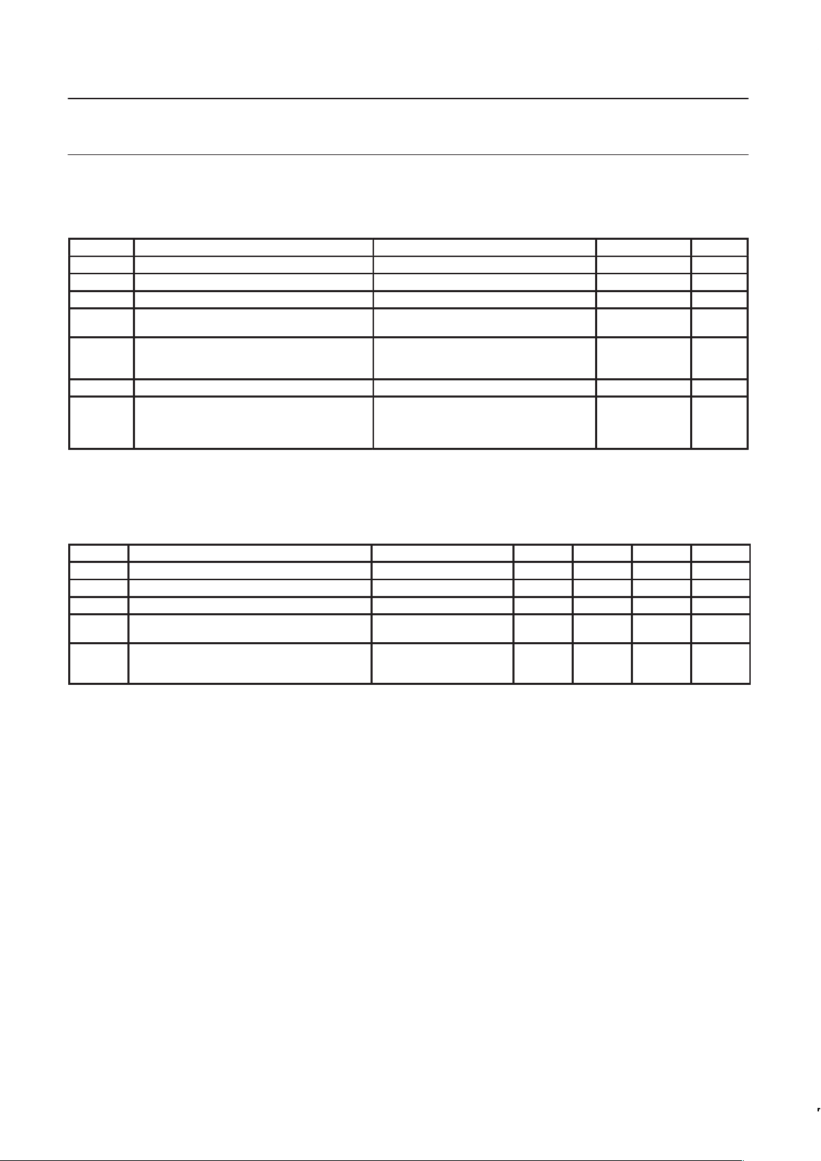
AC CHARACTERISTICS
GND = 0 V; tr = tf ≤ 2.5ns; CL = 50pF
LIMITS
CONDITION
–40 to +85 °C –40 to +125 °C
SYMBOL
PARAMETER
WAVEFORM
V
CC
(V)
MIN TYP1MAX MIN MAX
UNIT
1.2 90
Propagation delay
2.0 31 58 70
t
PHL/tPLH
gy
CP to QS
1
2.7 23 43 51
ns
3.0 to 3.6 17
2
34 41
1.2 80
Propagation delay
2.0 27 51 61
t
PHL/tPLH
gy
CP to QS
2
2.7 20 38 45
ns
3.0 to 3.6 14
2
30 36
1.2 115
Propagation delay
2.0 39 75 90
t
PHL/tPLH
gy
CP to QP
n
2.7 29 55 66
ns
3.0 to 3.6 22
2
44 53
1.2 105
Propagation delay
2.0 36 68 82
t
PHL/tPLH
gy
STR to QP
n
2.7 26 50 60
ns
3.0 to 3.6 20
2
40 48
1.2 100
3-State Output
2.0 34 65 77
t
PZH/tPZL
enable time
OE to QP
2.7 25 48 56
ns
Q
n
3.0 to 3.6 19
2
38 45
1.2 65
3-State Output
2.0 24 40 49
t
PHZ/tPLZ
disable time
OE to QP
2.7 18 32 37
ns
Q
n
3.0 to 3.6 14
2
26 30
2.0 34 9 41
t
w
Clock
pulse w
idth
2.7 25 6 30
ns
HIGH or LOW
3.0 to 3.6 20 5
2
24
2.0 34 9 41
t
w
Strob
e pulse w
idth
;
2.7 25 6 30
ns
HIGH
3.0 to 3.6 20 5
2
24
1.2 25
Set-up time
2.0 22 9 26
t
su
D to CP
2.7 16 6 19
ns
3.0 to 3.6 13 5
2
15
1.2 50
p
2.0 43 17 51
t
su
Set-u time
CP to STR
2.7 31 13 38
ns
3.0 to 3.6 25
10
NO TAG
30
Page 8

Philips Semiconductors Product specification
74LV40948-stage shift-and-store bus register
1998 Jun 23
8
SYMBOL UNIT
–40 to +125 °C–40 to +85 °C
CONDITION
WAVEFORMPARAMETER
SYMBOL UNIT
MAXMINMAXTYP
1
MIN
V
CC
(V)
WAVEFORMPARAMETER
1.2 –10
2.0 5 –4 5
T
h
Hold time
D to CP
2.7 5 –3 5
ns
3.0 to 3.6 5
–2
NO TAG
5
NOTES:
1. Unless otherwise stated, all typical values are measured at T
amb
= 25°C
2. Typical values are measured at V
CC
= 3.3 V.
Page 9

Philips Semiconductors Product specification
74LV40948-stage shift-and-store bus register
1998 Jun 23
9
AC CHARACTERISTICS (Continued)
GND = 0 V; tr = tf ≤ 2.5ns; CL = 50pF
CONDITION –40 to +85 °C –40 to +125 °C
SYMBOL PARAMETER WAVEFORM
V
CC
(V)
MIN TYP1MAX MIN MAX
UNIT
1.2 –25
Hold time
2.0 5 –9 5
T
h
D to STR
2.7 5 –6 5
ns
3.0 to 3.6 5 –5
2
5
2.0 14 52 12
f
max
Maxi
mum clock pulse
2.7 19 70 16
MHz
frequency
3.0 to 3.6 24 87
2
20
NOTES:
1. Unless otherwise stated, all typical values are measured at T
amb
= 25°C
2. Typical values are measured at V
CC
= 3.3 V.
AC WAVEFORMS
VM = 1.5 V at VCC ≥ 2.7 V
V
M
= 0.5 × V
CC
at VCC < 2.7 V.
V
OL
and VOH are the typical output voltage drop that occur with the output load.
V
X
= VOL + 0.3 V at V
CC
≥ 2.7 V
V
X
= VOL + 0.1 × VCC at VCC < 2.7 ς
V
Y
= VOH ± 0.3 V at V
CC
≥ 2.7 V
V
Y
= VOH ± 0.1 × V
CC
at VCC < 2.7V
SV01620
V
M
CP INPUT
QP
n
, QS
1
OUTPUT
QS
2
OUTPUT
V
M
V
M
t
PHL
t
PHL
t
PLH
t
PLH
t
W
1/f
max
V
CC
GND
V
OL
V
OL
V
OH
V
OH
Figure 1. Clock (CP) to output (QPn, QS1, QS2)
propagation delays, the clock pulse width
and the maximum clock frequency.
SV01619
V
M
CP INPUT
STR INPUT
QP
n
OUTPUT
V
M
V
M
t
h
t
su
t
W
t
PHL
t
PLH
V
CC
V
CC
GND
GND
V
OL
V
OH
Figure 2. Strobe (STR) to output (QPn) propagation delays and
the strobe pulse width and the clock set-up and hold times for
strobe input.
Page 10

Philips Semiconductors Product specification
74LV40948-stage shift-and-store bus register
1998 Jun 23
10
SV01618
outputs
disabled
outputs
enabled
outputs
enabled
t
PHZ
t
PZH
t
PZL
t
PLZ
V
X
V
Y
V
M
V
M
V
M
OE INPUT
OUTPUT
HIGH-to-OFF
OFF-to-HIGH
OUTPUT
LOW-to-OFF
OFF-to-LOW
GND
V
CC
V
CC
V
OL
V
OH
GND
Figure 3. 3-State enable and disable times for input OE.
SV01617
V
M
CP INPUT
D INPUT
QP
n
, QS1, QS2 OUTPUT
V
M
V
M
t
h
t
h
t
su
t
su
V
CC
V
CC
GND
GND
V
OL
V
OH
The shaded areas indicate when the input is permitted to change for predictable
output performance.
Figure 4. Data set-up and hold times for the data input (D).
TEST CIRCUIT
V
M
V
M
t
W
NEGATIVE
PULSE
10% 10%
90%
90%
0V
V
M
V
M
t
W
V
I
POSITIVE
PULSE
90% 90%
10%
10%
0V
t
THL
(t
f
)
t
TLH
(tr)t
THL
(tf)
t
TLH
(tr)
VM = 1.5V
Input Pulse Definition
SY00044
SWITCH POSITION
PULSE
GENERATOR
R
T
V
l
D.U.T.
V
O
CL= 50pF
R
L
= 1k
V
cc
Test Circuit for Outputs
Open
GND
S
1
V
S1
DEFINITIONS
V
CC
V
I
< 2.7V
2.7–3.6V
V
CC
2.7V
TEST S
1
t
PLZ/tPZL
t
PLH/tPHL
t
PHZ/tPZH
V
S1
Open
GND
V
S1
≥ 4.5 V
2 V
CC
V
CC
2 V
CC
RL = Load resistor
C
L
= Load capacitance includes jig and probe capacitance
R
T
= Termination resistance should be equal to Z
OUT
of
pulse generators.
V
I
2 V
CC
RL = 1k
Figure 5. Load circuitry for switching times.
Page 11

Philips Semiconductors Product specification
74LV40948-stage shift-and-store bus register
1998 Jun 23
11
DIP16: plastic dual in-line package; 16 leads (300 mil) SOT38-4
Page 12

Philips Semiconductors Product specification
74LV40948-stage shift-and-store bus register
1998 Jun 23
12
SO16: plastic small outline package; 16 leads; body width 3.9 mm SOT109-1
Page 13

Philips Semiconductors Product specification
74LV40948-stage shift-and-store bus register
1998 Jun 23
13
NOTES
Page 14

Philips Semiconductors Product specification
74LV40948-stage shift-and-store bus register
yyyy mmm dd
14
Definitions
Short-form specification — The data in a short-form specification is extracted from a full data sheet with the same type number and title. For
detailed information see the relevant data sheet or data handbook.
Limiting values definition — Limiting values given are in accordance with the Absolute Maximum Rating System (IEC 134). Stress above one
or more of the limiting values may cause permanent damage to the device. These are stress ratings only and operation of the device at these or
at any other conditions above those given in the Characteristics sections of the specification is not implied. Exposure to limiting values for extended
periods may affect device reliability.
Application information — Applications that are described herein for any of these products are for illustrative purposes only. Philips
Semiconductors make no representation or warranty that such applications will be suitable for the specified use without further testing or
modification.
Disclaimers
Life support — These products are not designed for use in life support appliances, devices or systems where malfunction of these products can
reasonably be expected to result in personal injury . Philips Semiconductors customers using or selling these products for use in such applications
do so at their own risk and agree to fully indemnify Philips Semiconductors for any damages resulting from such application.
Right to make changes — Philips Semiconductors reserves the right to make changes, without notice, in the products, including circuits, standard
cells, and/or software, described or contained herein in order to improve design and/or performance. Philips Semiconductors assumes no
responsibility or liability for the use of any of these products, conveys no license or title under any patent, copyright, or mask work right to these
products, and makes no representations or warranties that these products are free from patent, copyright, or mask work right infringement, unless
otherwise specified.
Philips Semiconductors
811 East Arques Avenue
P.O. Box 3409
Sunnyvale, California 94088–3409
Telephone 800-234-7381
Copyright Philips Electronics North America Corporation 1998
All rights reserved. Printed in U.S.A.
print code Date of release: 08-98
Document order number: 9397-750-04662
Data sheet
status
Objective
specification
Preliminary
specification
Product
specification
Product
status
Development
Qualification
Production
Definition
[1]
This data sheet contains the design target or goal specifications for product development.
Specification may change in any manner without notice.
This data sheet contains preliminary data, and supplementary data will be published at a later date.
Philips Semiconductors reserves the right to make chages at any time without notice in order to
improve design and supply the best possible product.
This data sheet contains final specifications. Philips Semiconductors reserves the right to make
changes at any time without notice in order to improve design and supply the best possible product.
Data sheet status
[1] Please consult the most recently issued datasheet before initiating or completing a design.
 Loading...