

Page 1
INTEGRATED CIRCUITS
74LV259
8-bit addressable latch
Product specification
Supersedes data of 1997 Jun 06
IC24 Data Handbook
1998 May 20
Page 2
Philips Semiconductors Product specification
74L V2598-bit addressable latch
FEA TURES
•Optimized for low voltage applications: 1.0 to 3.6 V
•Accepts TTL input levels between V
•Typical V
T
amb
•Typical V
T
amb
(output ground bounce) < 0.8 V at V
OLP
= 25°C
(output VOH undershoot) > 2 V at V
OHV
= 25°C
= 2.7 V and V
CC
CC
CC
•Combines demultiplexer and 8-bit latch
•Serial-to-parallel capability
•Output from each storage bit available
•Random (addressable) data entry
•Easily expandable
•Common reset input
•Useful as a 3-to-8 active HIGH decoder
•Output capability: standard
•I
category: MSI
CC
QUICK REFERENCE DATA
GND = 0 V; T
SYMBOL
t
PHL/tPLH
C
I
C
PD
NOTE:
1. C
is used to determine the dynamic power dissipation (PD in µW)
PD
= CPD × V
P
D
f
= input frequency in MHz; CL = output load capacity in pF;
i
= output frequency in MHz; VCC = supply voltage in V;
f
o
(C
L
= 25°C; tr = t
amb
Propagation delay
D, An to Q
LE to Q
n
MR to Q
Input capacitance 3.5 pF
Power dissipation capacitance per latch VI = GND to V
2
× fi (CL × V
CC
2
× V
× fo) = sum of the outputs.
CC
≤ 2.5 ns
f
PARAMETER CONDITIONS TYPICAL UNIT
n
n
2
× fo) where:
CC
= 3.6 V
CC
= 3.3 V,
= 3.3 V,
CL = 15 pF;
VCC = 3.3 V
DESCRIPTION
The 74LV259 is a low-voltage CMOS device and is pin and function
compatible with 74HC/HCT259.
The 74LV259 is a high-speed 8-bit addressable latch designed for
general purpose storage applications in digital systems. The
74LV259 is a multifunction device capable of storing single-line data
in eight addressable latches, and also 3-to-8 decoder and
demultiplexer , with active HIGH outputs (Q
available. The 74L V259 also incorporate an active LOW common
reset (MR
input (LE
the mode select table. In the addressable latch mode, data on the
data line (D) is written into the addressed latch. The addressed latch
will follow the data input with all non-addressed latches remaining in
their previous states. In the memory mode, all latches remain in their
previous states and are unaffected by the data or address inputs.
In the 3-to-8 decoding or demultiplexing mode, the addressed output
follows the state of the D input with all other outputs in the LOW
state. In the reset mode all outputs are LOW and unaffected by the
address (A
as an addressable latch, changing more than one bit of address
could impose a transient-wrong address. Therefore, this should only
be done while in the memory mode. The mode select table
summarizes the operations of the 74LV259.
CC
) for resetting all latches, as well as an active LOW enable
). The 74LV259 has four modes of operation as shown in
to A2) and date (D) input. When operating the 74LV259
0
1
to Q7), functions are
0
17
16
14
19 pF
ns
ORDERING INFORMATION
PACKAGES TEMPERATURE RANGE OUTSIDE NORTH AMERICA NORTH AMERICA PKG. DWG. #
16-Pin Plastic DIL –40°C to +125°C 74LV259 N 74LV259 N SOT38-4
16-Pin Plastic SO –40°C to +125°C 74LV259 D 74LV259 D SOT109-1
16-Pin Plastic SSOP Type II –40°C to +125°C 74LV259 DB 74LV259 DB SOT338-1
16-Pin Plastic TSSOP Type I –40°C to +125°C 74LV259 PW 74LV259PW DH SOT403-1
1998 May 20 853-1988 19420
2
Page 3
Philips Semiconductors Product specification
74LV2598-bit addressable latch
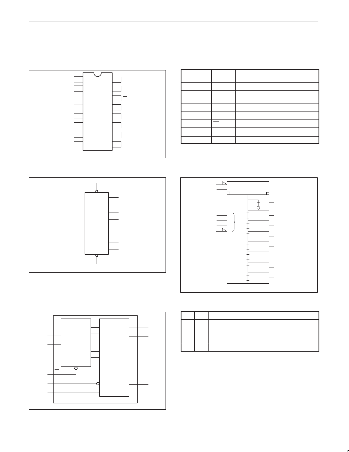
PIN CONFIGURATION
1
A
0
2
A
1
3
A
2
4
Q
0
5
Q
1
6
Q
2
7
Q
3
8
GND
LOGIC SYMBOL
13
1
2
3
PIN DESCRIPTION
16
15
14
13
12
11
10
9
SV01602
V
MR
LE
D
Q
Q
Q
Q
PIN
CC
NUMBER
1, 2, 3 A0 to A2Address inputs
4, 5, 6, 7, 9,
10, 11, 12
8 GND Ground (0 V)
7
6
5
13 D Data input
14 LE Latch enable input (active LOW)
15 MR Conditional reset input (active LOW)
16 V
4
SYMBOL FUNCTION
Q0 to Q7Latch outputs
CC
Positive supply voltage
LOGIC SYMBOL (IEEE/IEC)
14
LE
Q
D
Q
Q
Q
Q
A
0
Q
A
1
A
Q
2
Q
MR
15
0
1
2
3
4
5
6
7
SV01601
4
5
6
7
9
10
11
12
15
G8
13
Z9
9, 10D
DX
1
0
2
3
14
G
2
1 C10
0
1
0
7
2
3
4
5
6
7
4
8R
5
6
7
9
10
11
12
SV01603
FUNCTIONAL DIAGRAM
A
1
0
1-of–8
A
2
1
DECODER
A
3
2
14
LE
15
MR
13
D
1998 May 20
8 LATCHES
Q
0
Q
1
Q
2
Q
3
Q
4
Q
5
Q
6
Q
7
SV01604
MODE SELECT TABLE
LE MR MODE
4
5
6
7
9
10
11
12
L H Addressable latch
H H Memory
L L Active HIGH 8-channel demultiplexer
H L Reset
3
Page 4
Philips Semiconductors Product specification
OPERATING MODES
D
ltipl
(
)
()
(when D = H)
Addressable latch
74LV2598-bit addressable latch
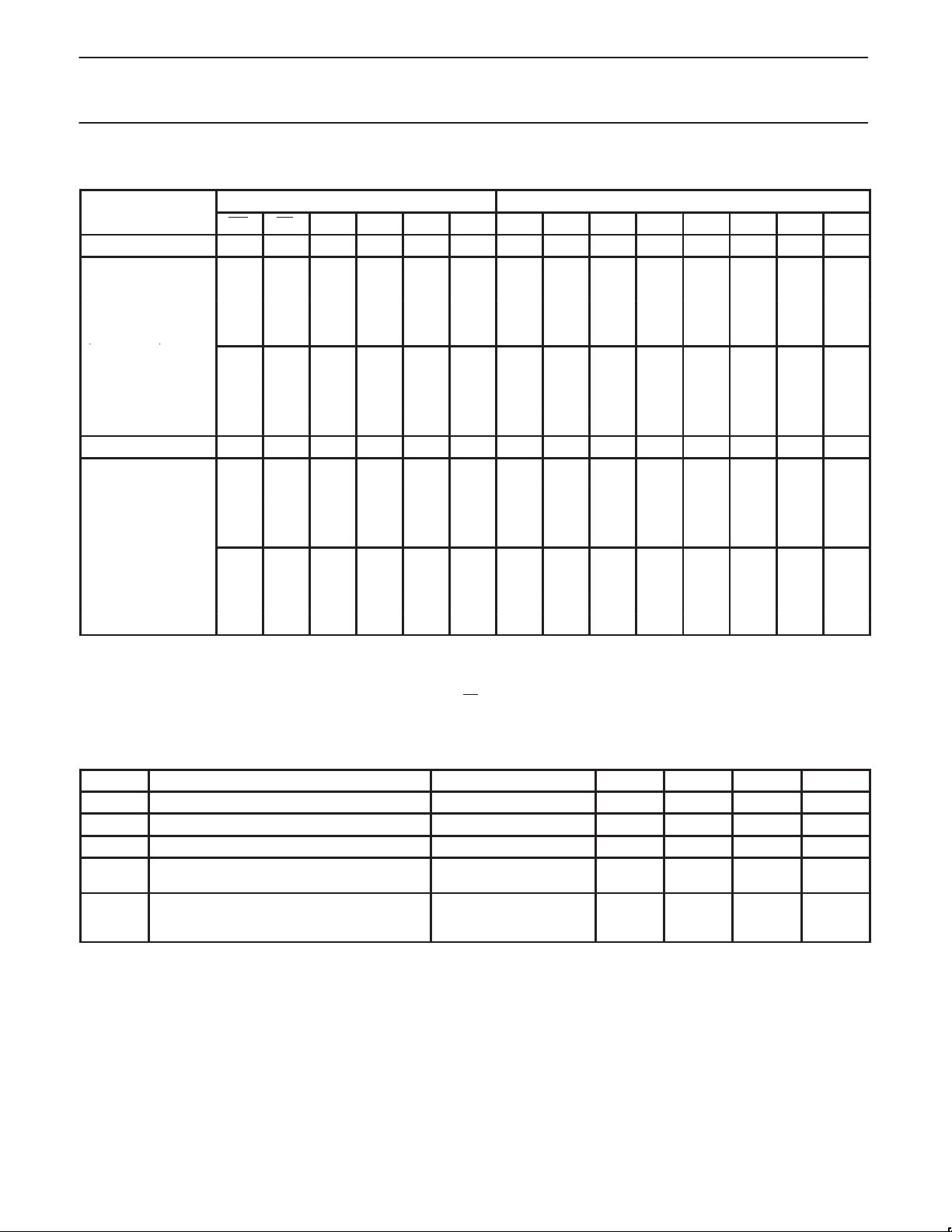
FUNCTION TABLE
INPUTS OUTPUTS
MR LE D A
Master reset L H X X X X L L L L L L L L
L L d L L L Q=d L L L L L L L
L L d H L L L Q=d L L L L L L
L L d L H L L L Q=d L L L L L
emu
active HIGH
ex
decoder
L L d H H L L L L Q=d L L L L
L L d L L H L L L L Q=d L L L
L L d H L H L L L L L Q=d L L
L L d L H H L L L L L L Q=d L
L L d H H H L L L L L L L Q=d
Store (do nothing) H H X X X X q0 q1 q2 q3 q4 q5 q6 q7
H L d L L L Q=d q1 q2 q3 q4 q5 q6 q7
H L d H L L q0 Q=d q2 q3 q4 q5 q6 q7
H L d L H L q0 q1 Q=d q3 q4 q5 q6 q7
H L d H H L q0 q1 q2 Q=d q4 q5 q6 q7
H L d L L H q0 q1 q2 q3 Q=d q5 q6 q7
H L d H L H q0 q1 q2 q3 q4 Q=d q6 q7
H L d L H H q0 q1 q2 q3 q4 q5 Q=q q7
H L d H H H q0 q1 q2 q3 q4 q5 q6 Q=d
NOTES:
H = HIGH voltage level
L = LOW voltage level
X = don’t care
d = HIGH or LOW data one set-up time prior to the LOW-to-HIGH LE
q = lower case letters indicate the state of the referenced output established during the last cycle established during the last cycle in which
it was addressed or cleared
A
0
A
1
Q
2
Q
0
Q
1
Q
2
Q
3
Q
4
Q
5
Q
6
7
transition
RECOMMENDED OPERATING CONDITIONS
SYMBOL PARAMETER CONDITIONS MIN TYP MAX UNIT
V
CC
V
I
V
O
T
amb
tr, t
f
NOTE:
1. The LV is guaranteed to function down to V
1998 May 20
DC supply voltage See Note 1 1.0 3.3 3.6 V
Input voltage 0 – V
Output voltage 0 – V
Operating ambient temperature range in free air
Input rise and fall times
= 1.0V (input levels GND or VCC); DC characteristics are guaranteed from VCC = 1.2V to VCC = 5.5V.
CC
See DC and AC
characteristics
VCC = 1.0V to 2.0V
VCC = 2.0V to 2.7V
VCC = 2.7V to 3.6V
–40
–40
–
–
–
–
–
–
CC
CC
+85
+125
500
200
100
ns/V
4
V
V
°C
Page 5
Philips Semiconductors Product specification
voltage
voltage
V
V
V
V
74LV2598-bit addressable latch
ABSOLUTE MAXIMUM RATINGS
1, 2
In accordance with the Absolute Maximum Rating System (IEC 134).
Voltages are referenced to GND (ground = 0 V).
SYMBOL
V
CC
I
IK
I
OK
I
O
I
GND
I
CC
T
stg
P
TOT
DC supply voltage –0.5 to +4.6 V
DC input diode current VI < –0.5 or VI > VCC + 0.5V 20 mA
DC output diode current VO < –0.5 or VO > VCC + 0.5V 50 mA
DC output source or sink current
– standard outputs
DC VCC or GND current for types with
,
– standard outputs
Storage temperature range –65 to +150 °C
Power dissipation per package
– plastic DIL
– plastic mini-pack (SO)
– plastic shrink mini-pack (SSOP and TSSOP)
PARAMETER CONDITIONS RATING UNIT
–0.5V < VO < VCC + 0.5V 25 mA
50 mA
for temperature range: –40 to +125°C
above +70°C derate linearly with 12 mW/K
above +70°C derate linearly with 8 mW/K
above +60°C derate linearly with 5.5 mW/K
750
500
400
mW
NOTES:
1. Stresses beyond those listed may cause permanent damage to the device. These are stress ratings only and functional operation of the
device at these or any other conditions beyond those indicated under “recommended operating conditions” is not implied. Exposure to
absolute-maximum-rated conditions for extended periods may affect device reliability .
2. The input and output voltage ratings may be exceeded if the input and output current ratings are observed.
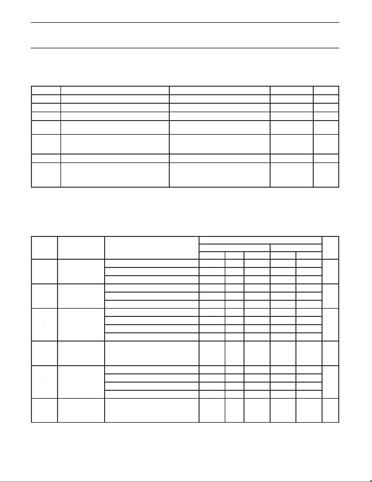
DC ELECTRICAL CHARACTERISTICS
Over recommended operating conditions. V oltages are referenced to GND (ground = 0 V).
LIMITS
SYMBOL P ARAMETER TEST CONDITIONS
VCC = 1.2 V 0.9 0.9
IH
HIGH level Input
V
VCC = 2.0 V 1.4 1.4
VCC = 2.7 to 3.6 V 2.0 2.0
VCC = 1.2 V 0.3 0.3
IL
LOW level Input
V
VCC = 2.0 V 0.6 0.6
VCC = 2.7 to 3.6 V 0.8 0.8
–IO = 100µA 1.2
IL;
–IO = 100µA 1.8 2.0 1.8
IL;
–IO = 100µA 2.5 2.7 2.5
IL;
–IO = 100µA 2.8 3.0 2.8
IL;
OH
HIGH level output
voltage; all outputs
VCC = 1.2 V; VI = VIH or V
VCC = 2.0 V; VI = VIH or V
VCC = 2.7 V; VI = VIH or V
VCC = 3.0 V; VI = VIH or V
HIGH level output
OH
voltage;
STANDARD
VCC = 3.0 V; VI = VIH or V
V
–IO = 6mA 2.40 2.82 2.20 V
IL;
outputs
IO = 100µA 0
IL;
IO = 100µA 0 0.2 0.2
IL;
IO = 100µA 0 0.2 0.2
IL;
IO = 100µA 0 0.2 0.2
IL;
LOW level output
OL
voltage; all outputs
VCC = 1.2 V; VI = VIH or V
VCC = 2.0 V; VI = VIH or V
VCC = 2.7 V; VI = VIH or V
VCC = 3.0 V; VI = VIH or V
LOW level output
OL
voltage;
STANDARD
VCC = 3.0 V; VI = VIH or V
V
IO = 6mA 0.25 0.40 0.50 V
IL;
outputs
-40°C to +85°C -40°C to +125°C
MIN TYP
1
MAX MIN MAX
UNIT
V
V
1998 May 20
5
Page 6

Philips Semiconductors Product specification
CONDITION
t
gy
Figure 2
ns
t
gy
Figure 3
ns
t
gy
Figure 1
ns
t
gy
Figure 4
ns
HIGH or LOW
LOW
t
Figure 5 and 6
ns
t
Figure 5
ns
74LV2598-bit addressable latch
DC ELECTRICAL CHARACTERISTICS (Continued)
Over recommended operating conditions. V oltages are referenced to GND (ground = 0 V).
LIMITS
SYMBOL P ARAMETER TEST CONDITIONS
Input leakage
I
I
current
CC
Quiescent supply
current; MSI
I
VCC = 3.6 V; VI = VCC or GND 1.0 1.0 µA
VCC = 3.6 V; VI = VCC or GND; IO = 0 20.0 160 µA
Additional quiescent
CC
supply current per
input
VCC = 2.7 V to 3.6 V; VI = VCC – 0.6 V 500 850 µA
∆I
NOTE:
1. All typical values are measured at T
amb
= 25°C.
AC CHARACTERISTICS
GND = 0V; tr = tf ≤ 2.5ns; CL = 50pF; RL = 1KΩ
SYMBOL PARAMETER WAVEFORM
PHL/tPLH
PHL/tPLH
PHL/tPLH
PHL
t
w
t
w
su
h
Propagation delay
D to Q
n
Propagation delay
An to Q
n
Propagation delay
LE to Q
n
Propagation delay
MR to Q
n
LE pulse width
MR pulse width
Set-up time
D, An to LE
Hold time
D to LE
Figure 1
Figure 4
VCC(V) MIN TYP1MAX MIN MAX
1.2 105
2.0 36 49 61
2.7 26 36 45
3.0 to 3.6 20
1.2 105
2.0 36 49 61
2.7 26 36 45
3.0 to 3.6 20
1.2 100
2.0 34 48 60
2.7 25 35 44
3.0 to 3.6 19
1.2 90
2.0 31 43 53
2.7 23 31 39
3.0 to 3.6 17
2.0 34 10 41
2.7 25 8 30
3.0 to 3.6 20 6
2.0 34 10 41
2.7 25 8 30
3.0 to 3.6 20 6
1.2 35
2.0 24 12 29
2.7 18 9 21
3.0 to 3.6 14 7
1.2 –30
2.0 5 –10 5
2.7 5 –8 5
3.0 to 3.6 5 –6
-40°C to +85°C -40°C to +125°C
MIN TYP
1
MAX MIN MAX
LIMITS
–40 to +85 °C –40 to +125 °C
2
29 36
2
29 36
2
28 35
2
25 31
2
2
2
2
24
24
17
5
UNIT
UNIT
ns
ns
1998 May 20
6
Page 7

Philips Semiconductors Product specification
SYMBOL
PARAMETER
WAVEFORM
UNIT
t
Figure 6
ns
74LV2598-bit addressable latch
AC CHARACTERISTICS (Continued)
GND = 0V; tr = tf ≤ 2.5ns; CL = 50pF; RL = 1KΩ
CONDITION –40 to +85 °C –40 to +125 °C
VCC(V) MIN TYP1MAX MIN MAX
1.2 –20
h
Hold time
An to LE
NOTES:
1. Unless otherwise stated, all typical values are measured at T
2. Typical values are measured at V
= 3.3 V.
CC
AC WAVEFORMS
VM = 1.5 V at VCC ≥ 2.7 V a n d ≤ 3.6V ;
= 0.5 ×V
V
M
V
and VOH are the typical output voltage drop that occur with the
OL
output load.
at VCC < 2.7 V a n d ≥ 4.5 V.
CC
amb
2.0 5 –7 5
2.7 5 –5 5
3.0 to 3.6 5 –4
2
= 25°C
V
CC
An INPUT
V
M
5
V
CC
D
INPUT
n
GND
V
CC
LE INPUT
GND
V
Qn OUTPUT
V
OH
OL
V
M
t
W
t
PHL
V
M
t
PLH
SV01605
Figure 1. Enable input (LE) to output (Qn) propagation delays
and the enable input pulse width.
V
CC
Dn INPUT
OUTPUT
Q
n
GND
V
V
t
PHL
OH
OL
V
M
t
PLH
V
M
SV01608
Figure 2. Data input (D) to output (Qn) propagation delays.
GND
t
PHL
V
OH
Qn OUTPUT
V
OL
V
M
Figure 3. Address inputs (An) to output (Qn)
propagation delays.
V
CC
MR INPUT
Q
OUTPUT
n
GND
V
V
OH
OL
V
M
t
W
t
PHL
V
M
Figure 4. Conditional reset input (MR) to output (Qn)
propagation delays.
t
PLH
SV01607
SV001606
1998 May 20
7
Page 8

Philips Semiconductors Product specification
74LV2598-bit addressable latch
AC WAVEFORMS (Continued)
VM = 1.5 V at VCC ≥ 2.7 V a n d ≤ 3.6V ;
= 0.5 ×V
V
M
V
and VOH are the typical output voltage drop that occur with the
OL
output load.
LE INPUT
Dn INPUT
Q
OUTPUT
n
The shaded areas indicate when the input is permitted
to change for predictable output performance
Figure 5. Data set-up and hold times for D input to LE input.
An INPUT
at VCC < 2.7 V a n d ≥ 4.5 V.
CC
V
CC
GND
V
CC
GND
V
OH
V
OL
V
CC
GND
V
CC
t
t
su
V
M
V
M
su
V
M
t
h
V
M
ADDRESS STABLE
t
su
Q = DQ = D
SV01609
t
h
t
h
TEST CIRCUIT
V
V
PULSE
GENERATOR
DEFINITIONS
= Load resistor
R
L
C
= Load capacitance includes jig and probe capacitance
L
RT = Termination resistance should be equal to Z
SWITCH POSITION
TEST S
t
PLH/tPHL
Figure 7. Load circuitry for switching times.
I
Open
D.U.T.
R
T
1
CC
V
OUT
V
CC
< 2.7V V
O
50pF
C
L
of pulse generators.
V
I
CC
2.7V2.7–3.6V
S
1
1k
1k
2 * V
Open
GND
SV00905
CC
LE INPUT
GND
The shaded areas indicate when the input is permitted to change for predictable
output performance.
V
M
SV01610
Figure 6. Address set-up and hold times for
A
inputs to LE input.
n
1998 May 20
8
Page 9

Philips Semiconductors Product specification
74LV2598-bit addressable latch
DIP16: plastic dual in-line package; 16 leads (300 mil) SOT38-4
1998 May 20
9
Page 10

Philips Semiconductors Product specification
74LV2598-bit addressable latch
SO16: plastic small outline package; 16 leads; body width 3.9 mm SOT109-1
1998 May 20
10
Page 11

Philips Semiconductors Product specification
74LV2598-bit addressable latch
SSOP16: plastic shrink small outline package; 16 leads; body width 5.3 mm SOT338-1
1998 May 20
11
Page 12

Philips Semiconductors Product specification
74LV2598-bit addressable latch
TSSOP16: plastic thin shrink small outline package; 16 leads; body width 4.4 mm SOT403-1
1998 May 20
12
Page 13

Philips Semiconductors Product specification
74LV2598-bit addressable latch
NOTES
1998 May 20
13
Page 14

Philips Semiconductors Product specification
74LV2598-bit addressable latch
DEFINITIONS
Data Sheet Identification Product Status Definition
Objective Specification
Preliminary Specification
Product Specification
Formative or in Design
Preproduction Product
Full Production
Philips Semiconductors and Philips Electronics North America Corporation reserve the right to make changes, without notice, in the products,
including circuits, standard cells, and/or software, described or contained herein in order to improve design and/or performance. Philips
Semiconductors assumes no responsibility or liability for the use of any of these products, conveys no license or title under any patent, copyright,
or mask work right to these products, and makes no representations or warranties that these products are free from patent, copyright, or mask
work right infringement, unless otherwise specified. Applications that are described herein for any of these products are for illustrative purposes
only. Philips Semiconductors makes no representation or warranty that such applications will be suitable for the specified use without further testing
or modification.
LIFE SUPPORT APPLICA TIONS
Philips Semiconductors and Philips Electronics North America Corporation Products are not designed for use in life support appliances, devices,
or systems where malfunction of a Philips Semiconductors and Philips Electronics North America Corporation Product can reasonably be expected
to result in a personal injury. Philips Semiconductors and Philips Electronics North America Corporation customers using or selling Philips
Semiconductors and Philips Electronics North America Corporation Products for use in such applications do so at their own risk and agree to fully
indemnify Philips Semiconductors and Philips Electronics North America Corporation for any damages resulting from such improper use or sale.
Philips Semiconductors
811 East Arques Avenue
P.O. Box 3409
Sunnyvale, California 94088–3409
Telephone 800-234-7381
This data sheet contains the design target or goal specifications for product development. Specifications
may change in any manner without notice.
This data sheet contains preliminary data, and supplementary data will be published at a later date. Philips
Semiconductors reserves the right to make changes at any time without notice in order to improve design
and supply the best possible product.
This data sheet contains Final Specifications. Philips Semiconductors reserves the right to make changes
at any time without notice, in order to improve design and supply the best possible product.
Copyright Philips Electronics North America Corporation 1998
All rights reserved. Printed in U.S.A.
print code Date of release: 05-96
Document order number: 9397-750-04442
1998 May 20
14
 Loading...