

Page 1
INTEGRATED CIRCUITS
74LV132
Quad 2-input NAND Schmitt-trigger
Product specification
Supersedes data of 1997 Feb 04
IC24 Data Handbook
1998 Apr 28
Page 2
Philips Semiconductors Product specification
74L V132Quad 2-input NAND Schmitt-trigger
FEA TURES
•Wide operating voltage: 1.0 to 5.5V
•Optimized for Low Voltage applications: 1.0 to 3.6V
•Accepts TTL input levels between V
•Typical V
T
amb
•Typical V
T
amb
(output ground bounce) 0.8V @ VCC = 3.3V,
OLP
= 25°C
(output VOH undershoot) 2V @ VCC = 3.3V,
OHV
= 25°C
= 2.7V and VCC = 3.6V
CC
•Output capability: standard
•I
category: SSI
CC
QUICK REFERENCE DATA
GND = 0V; T
SYMBOL
t
PHL/tPLH
C
I
C
PD
NOTES:
is used to determine the dynamic power dissipation (PD in µW)
1. C
PD
= CPD V
P
D
f
= input frequency in MHz; CL = output load capacitance in pF;
i
= output frequency in MHz; VCC = supply voltage in V;
f
o
(C
2. The condition is V
= 25°C; tr = tf 2.5 ns
amb
CC
2
V
L
fo) = sum of the outputs.
CC
PARAMETER CONDITIONS TYPICAL UNIT
Propagation delay
nA, nB to nY
Input capacitance 3.5 pF
Power dissipation capacitance per gate Notes 1 and 2 24 pF
2
fi (CL V
= GND to V
I
CC
2
fo) where:
CC
APPLICATIONS
•Wave and pulse shapers
•Astable multivibrators
•Monostable multivibrators
DESCRIPTION
The 74LV132 is a low-voltage Si-gate CMOS device and is pin and
function compatible with 74HC/HCT132.
The 74LV132 contains four 2-input NAND gates which accept
standard input signals. They are capable of transforming slowly
changing input signals into sharply defined, jitter-free output signals.
The gate switches at different points for positive and negative-going
signals. The difference between the positive voltage V
negative voltage V
CL = 15pF
VCC = 3.3V
is defined as the hysteresis voltage VH.
T–
10 ns
and the
T+
ORDERING INFORMATION
PACKAGES TEMPERATURE RANGE OUTSIDE NORTH AMERICA NORTH AMERICA PKG. DWG. #
14-Pin Plastic DIL –40°C to +125°C 74LV132 N 74LV132 N SOT27-1
14-Pin Plastic SO –40°C to +125°C 74LV132 D 74LV132 D SOT108-1
14-Pin Plastic SSOP Type II –40°C to +125°C 74LV132 DB 74LV132 DB SOT337-1
14-Pin Plastic TSSOP Type I –40°C to +125°C 74L V132 PW 74LV132PW DH SOT402-1
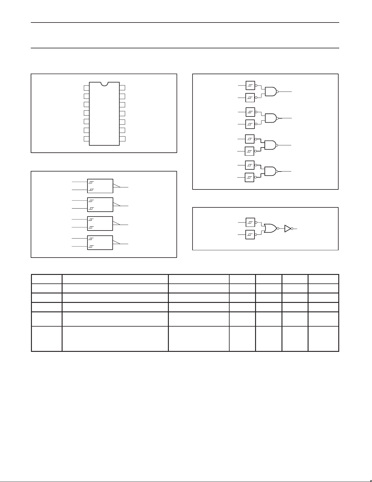
PIN DESCRIPTION
PIN
NUMBER
1, 4, 9, 12 1A to 4A Data inputs
2, 5, 10, 13 1B to 4B Data inputs
3, 6, 8, 11 1Y to 4Y Data outputs
7 GND Ground (0V)
14 V
SYMBOL FUNCTION
CC
Positive supply voltage
FUNCTION TABLE
INPUTS OUTPUT
nA nB nY
L L H
L H H
H L H
H H L
NOTES:
H = HIGH voltage level
L = LOW voltage level
1998 Apr 28 853–1912 19290
2
Page 3
Philips Semiconductors Product specification
74LV132Quad 2-input NAND Schmitt-trigger
PIN CONFIGURATION
1
1A
2
1B
1Y
3
2A
4
5
2B
6
2Y
GND
7
LOGIC SYMBOL (IEEE/IEC)
1
2
4
5
9
10
12
13
&
&
&
&
SV00213
SV00216
14
13
12
11
10
9
8 3Y
3
6
8
11
LOGIC SYMBOL
1A
V
CC
4B
4A
4Y
3B
3A
1
1B
2
2A
4
2B
5
3A
9
3B
10
4A
12
4B
13
1Y
2Y
3Y
4Y
SV00215
3
6
8
11
LOGIC DIAGRAM
A
B
Y
SV00217
RECOMMENDED OPERA TING CONDITIONS
SYMBOL PARAMETER CONDITIONS MIN TYP MAX UNIT
V
CC
V
V
T
amb
tr, t
NOTE:
1. The LV is guaranteed to function down to V
DC supply voltage See Note1 1.0 3.3 5.5 V
Input voltage 0 – V
I
Output voltage 0 – V
O
Operating ambient temperature range in free
air
Input rise and fall times except for
f
Schmitt-trigger inputs
= 1.0V (input levels GND or VCC); DC characteristics are guaranteed from VCC = 1.2V to VCC = 5.5V.
CC
See DC and AC
characteristics
VCC = 1.0V to 2.0V
VCC = 2.0V to 2.7V
VCC = 2.7V to 3.6V
VCC = 3.6V to 5.5V
–40
–40
–
–
–
–
–
–
–
–
CC
CC
+85
+125
500
200
100
50
V
V
°C
ns/V
1998 Apr 28
3
Page 4
Philips Semiconductors Product specification
V
V
V
V
voltage all out uts
V
g
V
voltage all out uts
74LV132Quad 2-input NAND Schmitt-trigger
ABSOLUTE MAXIMUM RATINGS
1, 2
In accordance with the Absolute Maximum Rating System (IEC 134).
Voltages are referenced to GND (ground = 0V).
SYMBOL
V
CC
±I
IK
±I
OK
±I
O
±I
GND
±I
CC
T
stg
P
TOT
DC supply voltage –0.5 to +7.0 V
DC input diode current VI < –0.5 or VI > VCC + 0.5V 20 mA
DC output diode current VO < –0.5 or VO > VCC + 0.5V 50 mA
DC output source or sink current
– standard outputs
DC VCC or GND current for types with
,
– standard outputs 50
Storage temperature range –65 to +150 °C
Power dissipation per package
– plastic DIL
– plastic mini-pack (SO)
– plastic shrink mini-pack (SSOP and TSSOP)
PARAMETER CONDITIONS RATING UNIT
–0.5V < VO < VCC + 0.5V
25
mA
mA
for temperature range: –40 to +125°C
above +70°C derate linearly with 12 mW/K
above +70°C derate linearly with 8 mW/K
above +60°C derate linearly with 5.5 mW/K
750
500
400
mW
NOTES:
1. Stresses beyond those listed may cause permanent damage to the device. These are stress ratings only and functional operation of the
device at these or any other conditions beyond those indicated under “recommended operating conditions” is not implied. Exposure to
absolute-maximum-rated conditions for extended periods may affect device reliability .
2. The input and output voltage ratings may be exceeded if the input and output current ratings are observed.
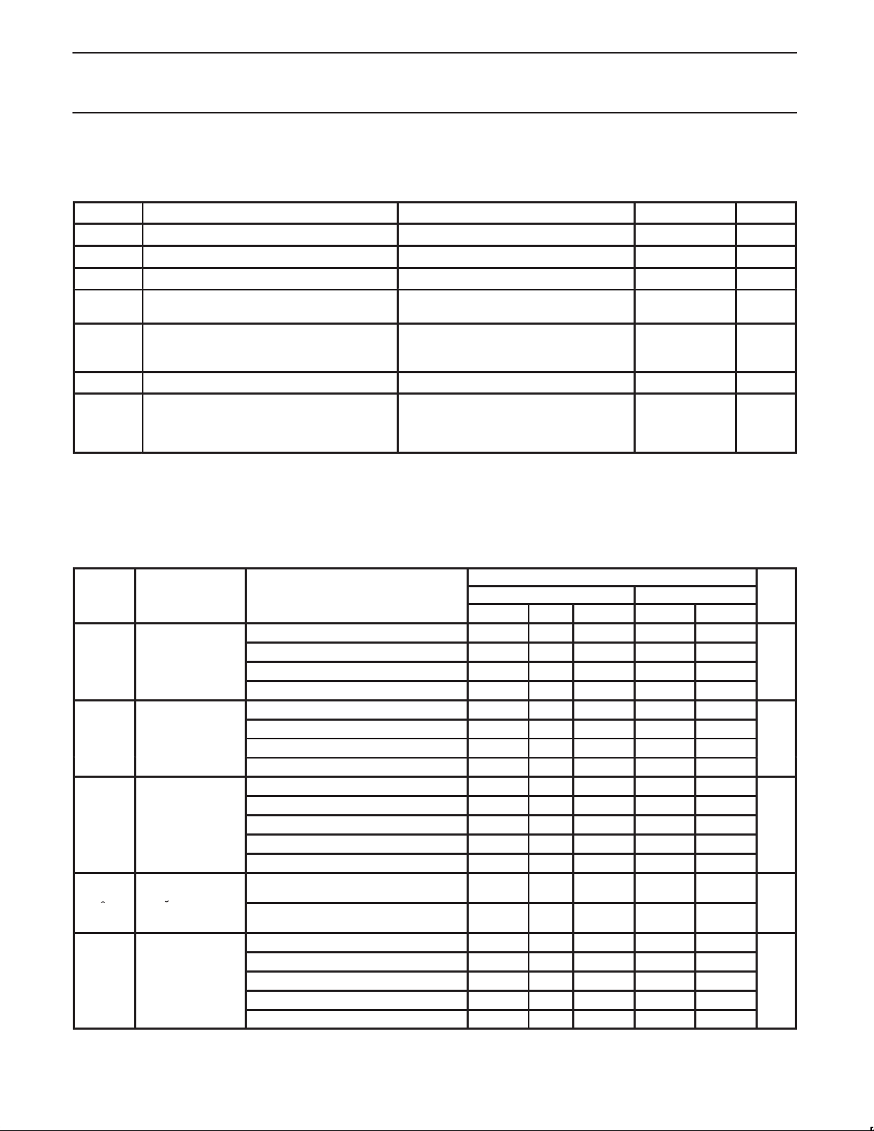
DC CHARACTERISTICS
Over recommended operating conditions. V oltages are referenced to GND (ground = 0V).
LIMITS
SYMBOL P ARAMETER TEST CONDITIONS
VCC = 1.2V 0.9 0.9
IH
HIGH level Input
voltage
VCC = 2.0V 1.4 1.4
VCC = 2.7 to 3.6V 2.0 2.0
VCC = 4.5 to 5.5V 0.7*V
VCC = 1.2V 0.3 0.3
IL
LOW level Input
voltage
VCC = 2.0V 0.6 0.6
VCC = 2.7 to 3.6V 0.8 0.8
VCC = 4.5 to 5.5 0.3*V
VCC = 1.2V; VI = VIH or V
VCC = 2.0V; VI = VIH or V
OH
HIGH level output
;
V
VCC = 2.7V; VI = VIH or V
p
VCC = 3.0V; VI = VIH or V
VCC = 4.5V; VI = VIH or V
OH
HIGH level output
voltage;
STANDARD
outputs
VCC = 3.0V; VI = VIH or V
VCC = 4.5V; VI = VIH or V
VCC = 1.2V; VI = VIH or V
VCC = 2.0V; VI = VIH or V
OL
LOW level output
;
V
VCC = 2.7V; VI = VIH or V
p
VCC = 3.0V; VI = VIH or V
VCC = 4.5V; VI = VIH or V
–IO = 100µA 1.2
IL;
–IO = 100µA 1.8 2.0 1.8
IL;
–IO = 100µA 2.5 2.7 2.5
IL;
–IO = 100µA 2.8 3.0 2.8
IL;
–IO = 100µA 4.3 4.5 4.3
IL;
–IO = 6mA 2.40 2.82 2.20
IL;
–IO = 12mA 3.60 4.20 3.50
IL;
IO = 100µA 0
IL;
IO = 100µA 0 0.2 0.2
IL;
IO = 100µA 0 0.2 0.2
IL;
IO = 100µA 0 0.2 0.2
IL;
IO = 100µA 0 0.2 0.2
IL;
-40°C to +85°C -40°C to +125°C
MIN TYP
CC
1
MAX MIN MAX
0.7*V
CC
CC
0.3*V
CC
UNIT
V
V
1998 Apr 28
4
Page 5

Philips Semiconductors Product specification
SYMBOL
PARAMETER
TEST CONDITIONS
UNIT
V
g
V
CONDITION
threshold
1 and 2
threshold
1 and 2
(V
T+
V
T
)
1 and 2
74LV132Quad 2-input NAND Schmitt-trigger
DC CHARACTERISTICS (Continued)
Over recommended operating conditions. V oltages are referenced to GND (ground = 0V).
LIMITS
-40°C to +85°C -40°C to +125°C
LOW level output
voltage;
OL
STANDARD
outputs
Input leakage
I
I
current
CC
Quiescent supply
current; SSI
I
VCC = 3.0V; VI = VIH or V
VCC = 4.5V; VI = VIH or V
VCC = 5.5V; VI = VCC or GND 1.0 1.0 µA
VCC = 5.5V; VI = VCC or GND; IO = 0 20.0 40 µA
Additional
CC
quiescent supply
current per input
VCC = 2.7V to 3.6V; VI = VCC – 0.6V 500 850 µA
∆I
NOTE:
1. All typical values are measured at T
amb
= 25°C.
TRANSFER CHARACTERISTICS
Voltages are referenced to GND = 0V.
SYMBOL PARAMETER WAVEFORM
V
T+
V
T–
V
H
Positive going
Negative going
Hysteresis
–
–
NOTE:
1. Unless otherwise stated, all typical values are at T
Figures
Figures
Figures
amb
IO = 6mA 0.25 0.40 0.50
IL;
IO = 12mA 0.35 0.55 0.65
IL;
LIMITS
–40 to +85°C –40 to +125°C
VCC(V) MIN TYP1MAX MIN MAX
1.2 – 0.70 – –
2.0 0.8 1.10 1.4 0.8 1.4
2.7 1.0 1.45 2.0 1.0 2.0
3.0 1.2 1.60 2.2 1.2 2.2
3.6 1.5 1.95 2.4 1.5 2.4
4.5 1.7 2.50 3.2 1.7 3.2
5.5 2.1 3.00 3.9 2.1 3.9
1.2 – 0.34 – – –
2.0 0.3 0.65 0.9 0.3 0.9
2.7 0.4 0.90 1.4 0.4 1.4
3.0 0.6 1.05 1.5 0.6 1.5
3.6 0.8 1.30 1.8 0.8 1.8
4.5 0.9 1.60 2.0 0.9 2.0
5.5 1.2 2.00 2.6 1.2 2.6
1.2 – 0.30 – – –
2.0 0.2 0.55 0.8 0.2 0.8
2.7 0.3 0.60 1.1 0.3 1.1
3.0 0.4 0.65 1.2 0.4 1.2
3.6 0.4 0.70 1.2 0.4 1.2
4.5 0.4 0.80 1.4 0.4 1.4
5.5 0.6 1.00 1.5 0.6 1.5
= 25°C.
UNIT
V
V
V
1998 Apr 28
5
Page 6

Philips Semiconductors Product specification
CONDITION
nA, nB, to nY
74LV132Quad 2-input NAND Schmitt-trigger
AC CHARACTERISTICS
GND = 0V; tr = tf = 2.5ns; CL = 50pF
LIMITS
SYMBOL PARAMETER WAVEFORM
t
PHL/tPLH
Propagation delay
Figure 6
NOTES:
1. Unless otherwise stated, all typical values are at T
2. Typical value measured at V
3. Typical value measured at V
= 3.3V.
CC
= 5.0V.
CC
amb
= 25°C.
TRANSFER CHARACTERISTIC W AVEFORMS
–40 to +85°C –40 to +125°C
VCC(V) MIN TYP1MAX MIN MAX
1.2 – 65 – – –
2.0 – 18 34 – 43
2.7 – 15 24 – 30
3.0 to 3.6 – 12
4.5 to 5.5 – 9.0
2
20 – 25
2
14 – 17
UNIT
ns
V
O
V
H
V
T–
V
T+
SV00218
Figure 1. Transfer characteristic.
V
V
I
V
O
T+
V
M
V
T–
SV00220
Figure 2. Definition of VT+, VT– and VH; where VT+ and VT– are
between limits of 20% and 70%.
10
I
CC
(µA)
8
6
4
2
0
0 0.3 0.6 0.9 1.2
VIN (V)
SV00222
Figure 3. Typical LV132 transfer characteristics; VCC = 1.2V.
100
I
CC
(µA)
80
60
40
20
1998 Apr 28
0
0
0.4 0.8 1.2 1.6
(V)
V
IN
Figure 4. Typical LV132 transfer characteristics; VCC = 2.0V.
6
2.0
SV00224
Page 7

Philips Semiconductors Product specification
74LV132Quad 2-input NAND Schmitt-trigger
TRANSFER CHARACTERISTIC W AVEFORMS
(Continued)
250
I
CC
(µA)
200
150
100
50
0
0 0.6
1.2
1.8
V
(V)
IN
2.4
SV00225
Figure 5. Typical LV132 transfer characteristics; VCC = 3.0V.
AC WAVEFORMS
VM = 1.5V at VCC 2.7V 3.6V
= 0.5V * VCC at V
V
M
V
and V
OL
output load.
are the typical output voltage drop that occur with the
OH
2.7V and 4.5V
CC
3.0
TEST CIRCUIT
V
cc
V
PULSE
GENERATOR
DEFINITIONS
RL = Load resistor
CL = Load capacitance includes jig and probe capacitiance
RT = Termination resistance should be equal to Z
TEST
t
PLH/tPHL
Figure 7.Load circuitry for switching times.
l
D.U.T.
R
T
Test Circuit for Outputs
V
CC
< 2.7V
2.7–3.6V
≥ 4.5 V V
V
V
2.7V
CC
CC
V
O
50pF
C
L
of pulse generators.
OUT
I
RL= 1k
SV00902
V
CC
nA, nB INPUT
GND
V
OH
nY OUTPUT
V
OL
V
M
t
PHL
V
M
t
PLH
V
M
SV00219
Figure 6. Input (nA, nB) to output (nY) propagation delays.
1998 Apr 28
7
Page 8

Philips Semiconductors Product specification
Quad 2-input NAND Schmitt-trigger
DIP14: plastic dual in-line package; 14 leads (300 mil) SOT27-1
74LV132
1998 Apr 28
8
Page 9

Philips Semiconductors Product specification
Quad 2-input NAND Schmitt-trigger
SO14: plastic small outline package; 14 leads; body width 3.9 mm SOT108-1
74LV132
1998 Apr 28
9
Page 10

Philips Semiconductors Product specification
Quad 2-input NAND Schmitt-trigger
SSOP14: plastic shrink small outline package; 14 leads; body width 5.3 mm SOT337-1
74LV132
1998 Apr 28
10
Page 11

Philips Semiconductors Product specification
Quad 2-input NAND Schmitt-trigger
TSSOP14: plastic thin shrink small outline package; 14 leads; body width 4.4 mm SOT402-1
74LV132
1998 Apr 28
11
Page 12

Philips Semiconductors Product specification
74LV132Quad 2-input NAND Schmitt-trigger
Data sheet status
Data sheet
status
Objective
specification
Preliminary
specification
Product
specification
Product
status
Development
Qualification
Production
Definition
This data sheet contains the design target or goal specifications for product development.
Specification may change in any manner without notice.
This data sheet contains preliminary data, and supplementary data will be published at a later date.
Philips Semiconductors reserves the right to make chages at any time without notice in order to
improve design and supply the best possible product.
This data sheet contains final specifications. Philips Semiconductors reserves the right to make
changes at any time without notice in order to improve design and supply the best possible product.
[1]
[1] Please consult the most recently issued datasheet before initiating or completing a design.
Definitions
Short-form specification — The data in a short-form specification is extracted from a full data sheet with the same type number and title. For
detailed information see the relevant data sheet or data handbook.
Limiting values definition — Limiting values given are in accordance with the Absolute Maximum Rating System (IEC 134). Stress above one
or more of the limiting values may cause permanent damage to the device. These are stress ratings only and operation of the device at these or
at any other conditions above those given in the Characteristics sections of the specification is not implied. Exposure to limiting values for extended
periods may affect device reliability.
Application information — Applications that are described herein for any of these products are for illustrative purposes only. Philips
Semiconductors make no representation or warranty that such applications will be suitable for the specified use without further testing or
modification.
Disclaimers
Life support — These products are not designed for use in life support appliances, devices or systems where malfunction of these products can
reasonably be expected to result in personal injury . Philips Semiconductors customers using or selling these products for use in such applications
do so at their own risk and agree to fully indemnify Philips Semiconductors for any damages resulting from such application.
Right to make changes — Philips Semiconductors reserves the right to make changes, without notice, in the products, including circuits, standard
cells, and/or software, described or contained herein in order to improve design and/or performance. Philips Semiconductors assumes no
responsibility or liability for the use of any of these products, conveys no license or title under any patent, copyright, or mask work right to these
products, and makes no representations or warranties that these products are free from patent, copyright, or mask work right infringement, unless
otherwise specified.
Philips Semiconductors
811 East Arques Avenue
P.O. Box 3409
Sunnyvale, California 94088–3409
Telephone 800-234-7381
Copyright Philips Electronics North America Corporation 1998
All rights reserved. Printed in U.S.A.
print code Date of release: 08-98
Document order number: 9397-750-04422
yyyy mmm dd
12
 Loading...