

Page 1

INTEGRATED CIRCUITS
74LV123
Dual retriggerable monostable
multivibrator with reset
Product specification
Supersedes data of 1997 Feb 04
IC24 Data Handbook
1998 Apr 20
Page 2
Philips Semiconductors Product specification
Dual retriggerable monostable multivibrator
with reset
FEA TURES
•Optimized for Low Voltage applications: 1.0 to 5.5V
•Accepts TTL input levels between V
•Typical V
T
amb
•Typical V
T
amb
(output ground bounce) 0.8V @ VCC = 3.3V,
OLP
= 25°C
(output VOH undershoot) 2V @ VCC = 3.3V,
OHV
= 25°C
= 2.7V and VCC = 3.6V
CC
•DC triggered from active HIGH or active LOW inputs
•Retriggerable for very long pulses up to 100% duty factor
•Direct reset terminates output pulses
•Schmitt-trigger action on all inputs except for the reset input
•Output capability: standard (except for nR
•I
category: MSI
CC
EXT/CEXT
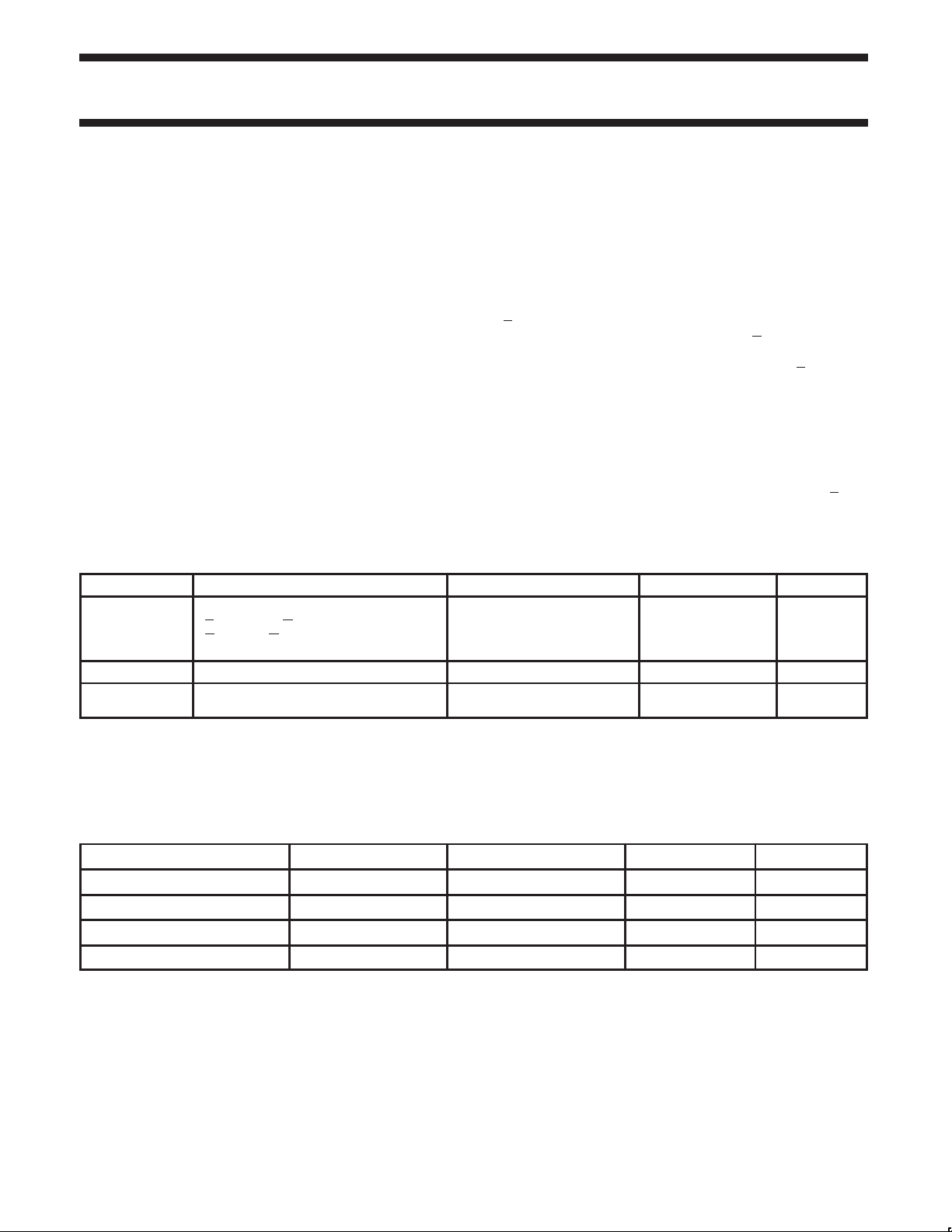
QUICK REFERENCE DATA
GND = 0V; T
SYMBOL
t
PHL/tPLH
C
I
C
PD
NOTES:
1. C
is used to determine the dynamic power dissipation (PD in µW)
PD
= CPD V
P
D
f
= input frequency in MHz; CL = output load capacitance in pF;
i
= output frequency in MHz; VCC = supply voltage in V;
f
o
(C
= 25°C; tr = tf 2.5 ns
amb
CC
2
V
L
fo) = sum of the outputs.
CC
PARAMETER CONDITIONS TYPICAL UNIT
Propagation delay
nA, nB to nQ, nQ
nRD to nQ, nQ
Input capacitance 3.5 pF
Power dissipation capacitance per monost-
able
2
fi (CL V
2
fo) where:
CC
)
DESCRIPTION
The 74LV123 is a low-voltage Si-gate CMOS device and is pin and
function compatible with the 74HC/HCT123.
The 74LV123 is a dual retriggerable monostable multivibrator with
output pulse width control by three methods. The basic pulse time is
programmed by selection of an external resistor (R
capacitor (C
Figure 1. Once triggered, the basic output pulse width may be
extended by retriggering the gated active LOW-going edge input
(nA
process, the output pulse period (nQ = HIGH, nQ
made as long as desired. Alternatively, an output delay can be
terminated at any time by a LOW-going edge on input nR
also inhibits the triggering. Figures 1 and 2 illustrate pulse control by
retriggering and early reset. The basic output pulse width is
essentially determined by the values of the external timing
components R
see Figure 5. When C
width is defined as: t
t
= pulse width in ns; R
W
C
EXT
nB inputs makes the circuit highly tolerant of slower input rise and
fall times.
CL = 15pF
V
= 3.3V
CC
= 5KΩ
R
EXT
C
= 0pF
EXT
VCC = 3.3V, VI = GND to V
74L V123
) and
). They are normally connected as shown in
EXT
) or the active HIGH-going edge input (nB). By repeating this
and C
EXT
= external capacitor in pF. Schmitt-trigger action in the nA and
CC
. For pulse width when C
EXT
10,000pF, the typical output pulse
EXT
= 0.45 R
W
= external resistor in KΩ; and
EXT
1
C
EXT
25
20
60 pF
EXT
= LOW) can be
EXT
(typ.), where
EXT
, which
D
<10000pF,
ns
ns
ORDERING INFORMATION
PACKAGES TEMPERATURE RANGE OUTSIDE NORTH AMERICA NORTH AMERICA PKG. DWG. #
16-Pin Plastic DIL –40°C to +125°C 74LV123 N 74LV123 N SOT38-1
16-Pin Plastic SO –40°C to +125°C 74LV123 D 74LV123 D SOT109-1
16-Pin Plastic SSOP Type II –40°C to +125°C 74LV123 DB 74LV123 DB SOT338-1
16-Pin Plastic TSSOP Type I –40°C to +125°C 74L V123 PW 74LV123PW DH SOT403-1
1998 Apr 28 853–191 1 19290
2
Page 3

Philips Semiconductors Product specification
Dual retriggerable monostable multivibrator
with reset
PIN CONFIGURATION
SV00096
16
V
CC
15
1R
EXT/CEXT
14
1C
EXT
13
1Q
12
2Q
11
2R
D
10
2B
9
2A
13
4
5
12
1
1A
1B
2
1R
3
D
1Q
4
5
2Q
2C
6
EXT
GND
7
8
2R
EXT/CEXT
PIN DESCRIPTION
PIN
NUMBER
1,9 1A, 2A
2,10 1B, 2B
3,11 1RD, 2R
4, 12 1Q, 2Q Outputs (active LOW)
7 2R
8 GND Ground (0V)
13, 5 1Q, 2Q Outputs (active HIGH)
14, 6
15 1R
16 V
SYMBOL FUNCTION
Trigger inputs
(negative-edge triggered)
Trigger inputs
(positive-edge triggered)
Direct reset LOW and trigger action at
D
positive edge
EXT/CEXT
1C
EXT,
2C
EXT
EXT/CEXT
CC
External resistor/capacitor connection
External capacitor connection
External resistor/capacitor connection
Positive supply voltage
LOGIC SYMBOL (IEEE/IEC)
14
15
1
2
3
6
7
9
10
CX
RCX
&
R
CX
RCX
&
LOGIC SYMBOL
1A
1
9
2A
1B
2
2B
10
1R
3
D
11
2R
D
FUNCTIONAL DIAGRAM
1A
1
2A
9
1B
2
2B
10
1R
3
D
11
2R
D
74LV123
14
1C
EXT
2C
6
EXT
1R
EXT/CEXT
2R
EXT/CEXT
S
Q
T
Q
R
D
1R
EXT/CEXT
2R
EXT/CEXT
S
Q
T
Q
R
D
1Q
2Q
1Q
2Q
SV00097
1C
EXT
2C
EXT
1Q
2Q
1Q
2Q
SV00099
15
7
13
5
4
12
14
6
15
7
13
5
4
12
1998 Apr 28
11
R
SV00098
3
Page 4

Philips Semiconductors Product specification
Dual retriggerable monostable multivibrator
with reset
LOGIC DIAGRAM
R
D
RR
CLCLV
CC
V
CC
CL
R
nR
V
CC
74LV123
EXT/CEXT
Q
Q
A
B
R
It is recommended that Pin 6 (2C
) and Pin 14 (1C
EXT
CLCL
FUNCTION TABLE
INPUTS OUTPUTS
nR
D
L X X L H
X H X L * H *
X X L L * H *
H L ↑
H ↓ H
↑ L H
NOTES:
* If the monostable was triggered before this condition was
established, the pulse will continue as programmed.
H = HIGH voltage level
L = LOW voltage level
X = don’t care
↑ = LOW-to-HIGH transition
↓ = HIGH-to-LOW transition
= one HIGH level output pulse
= one LOW level output pulse
nA nB nQ nQ
) by externally grounded to Pin 8 (GND)
EXT
to nC
(pin 14 or 6)
Figure 1.Timing component connection
EXT
SV00100
V
CC
R
EXT
C
EXT
to nR
EXT/CEXT
(pin 15 or 7)
SV00101
1998 Apr 28
4
Page 5
Philips Semiconductors Product specification
Dual retriggerable monostable multivibrator
74LV123
with reset
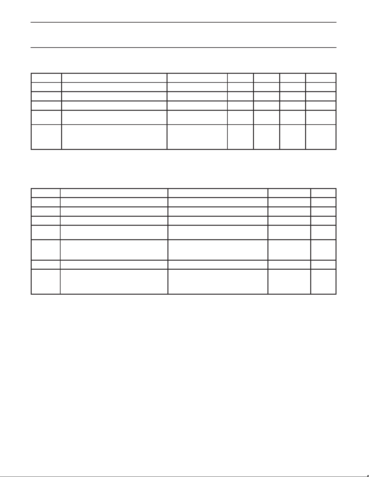
RECOMMENDED OPERATING CONDITIONS
SYMBOL PARAMETER CONDITIONS MIN TYP MAX UNIT
1
1.0 3.3 5.5 V
CC
CC
–40
–40
–
–
–
–
–
–
–
–
+85
+125
500
200
100
50
25
T
V
V
tr, t
CC
V
amb
DC supply voltage See Note
Input voltage 0 – V
I
Output voltage 0 – V
O
Operating ambient temperature range in free
air
Input rise and fall times except for
f
Schmitt-trigger inputs
NOTE:
1. The LV is guaranteed to function down to V
ABSOLUTE MAXIMUM RATINGS
= 1.0V (input levels GND or VCC); DC characteristics are guaranteed from VCC = 1.2V to VCC = 5.5V.
CC
1, 2
In accordance with the Absolute Maximum Rating System (IEC 134).
Voltages are referenced to GND (ground = 0V).
SYMBOL
V
CC
I
IK
I
OK
I
O
DC supply voltage –0.5 to +7.0 V
DC input diode current VI < –0.5 or VI > VCC + 0.5V 20 mA
DC output diode current VO < –0.5 or VO > VCC + 0.5V 50 mA
DC output source or sink current
– standard outputs
PARAMETER CONDITIONS RATING UNIT
–0.5V < VO < VCC + 0.5V
See DC and AC
characteristics
VCC = 1.0V to 2.0V
VCC = 2.0V to 2.7V
VCC = 2.7V to 3.6V
VCC = 3.6V to 5.5V
V
V
°C
ns/V
mA
I
I
P
GND
T
TOT
stg
DC VCC or GND current for types with
,
– standard outputs 50
CC
Storage temperature range –65 to +150 °C
Power dissipation per package
– plastic DIL
– plastic mini-pack (SO)
– plastic shrink mini-pack (SSOP and TSSOP)
for temperature range: –40 to +125°C
above +70°C derate linearly with 12 mW/K
above +70°C derate linearly with 8 mW/K
above +60°C derate linearly with 5.5 mW/K
750
500
500
mA
mW
NOTES:
1. Stresses beyond those listed may cause permanent damage to the device. These are stress ratings only and functional operation of the
device at these or any other conditions beyond those indicated under “recommended operating conditions” is not implied. Exposure to
absolute-maximum-rated conditions for extended periods may affect device reliability .
2. The input and output voltage ratings may be exceeded if the input and output current ratings are observed.
1998 Apr 28
5
Page 6

Philips Semiconductors Product specification
V
V
V
V
voltage all out uts
V
g
V
voltage all out uts
V
g
V
Dual retriggerable monostable multivibrator
with reset
DC ELECTRICAL CHARACTERISTICS
Over recommended operating conditions. V oltages are referenced to GND (ground = 0V).
SYMBOL P ARAMETER TEST CONDITIONS
VCC = 1.2V 0.9 0.9
IH
HIGH level Input
voltage
VCC = 2.0V 1.4 1.4
VCC = 2.7 to 3.6V 2.0 2.0
VCC = 4.5 to 5.5V 0.7V
VCC = 1.2V 0.3 0.3
IL
LOW level Input
voltage
VCC = 2.0V 0.6 0.6
VCC = 2.7 to 3.6V 0.8 0.8
VCC = 4.5 to 5.5 0.3V
VCC = 1.2V; VI = VIH or V
VCC = 2.0V; VI = VIH or V
OH
HIGH level output
;
V
VCC = 2.7V; VI = VIH or V
p
VCC = 3.0V; VI = VIH or V
VCC = 4.5V; VI = VIH or V
OH
HIGH level output
voltage;
STANDARD
outputs
VCC = 3.0V; VI = VIH or V
VCC = 4.5V; VI = VIH or V
VCC = 1.2V; VI = VIH or V
VCC = 2.0V; VI = VIH or V
OL
LOW level output
;
V
VCC = 2.7V; VI = VIH or V
p
VCC = 3.0V; VI = VIH or V
VCC = 4.5V; VI = VIH or V
LOW level output
voltage;
OL
STANDARD
outputs
Input leakage
I
I
current
CC
Quiescent supply
current; MSI
I
VCC = 3.0V; VI = VIH or V
VCC = 4.5V; VI = VIH or V
VCC = 5.5V; VI = VCC or GND 1.0 1.0 µA
VCC = 5.5V; VI = VCC or GND; IO = 0 20.0 160 µA
IL;
IL;
IL;
IL;
IL;
IL;
IL;
IL;
IL;
IL;
IL;
IL;
IL;
IL;
Additional
CC
quiescent supply
current
VCC = 2.7V to 3.6V; VI = VCC – 0.6V 500 850 µA
∆I
NOTES:
1. All typical values are measured at T
amb
= 25°C.
–IO = 100µA 1.2
–IO = 100µA 1.8 2.0 1.8
–IO = 100µA 2.5 2.7 2.5
–IO = 100µA 2.8 3.0 2.8
–IO = 100µA 4.3 4.5 4.3
–IO = 6mA 2.40 2.82 2.20
–IO = 12mA 3.60 4.20 3.50
IO = 100µA 0
IO = 100µA 0 0.2 0.2
IO = 100µA 0 0.2 0.2
IO = 100µA 0 0.2 0.2
IO = 100µA 0 0.2 0.2
IO = 6mA 0.25 0.40 0.50
IO = 12mA 0.35 0.55 0.65
-40°C to +85°C -40°C to +125°C
MIN TYP
CC
LIMITS
1
MAX MIN MAX
0.7V
CC
74LV123
CC
0.3V
UNIT
CC
V
V
1998 Apr 28
6
Page 7

Philips Semiconductors Product specification
CONDITION
P
Figure 3
nR
D
nQ
R
P
Figure 3
nR
D
nQ
R
P
Figure 3
nR
D
(reset)
R
P
Figure 3
nR
D
(reset)
R
t
gg
Figure 3
ns
t
gg
Figure 3
ns
t
Figure 2
ns
t
nQ
HIGH
C
100nF
µs
Q
EXT
t
nQ
HIGH
C
0F
ns
Q
EXT
t
gg
C
0F
ns
EXT
Dual retriggerable monostable multivibrator
with reset
AC CHARACTERISTICS
GND = 0V; tr = tf ≤ 2.5ns; CL = 50pF; RL =1 KΩ
SYMBOL PARAMETER WAVEFORM
VCC(V) MIN TYP
1.2 120
2.0 40 76 92
2.7 30 56 68
3.0 to 3.6 25
4.5 to 5.5 18
1.2 120
2.0 40 76 92
2.7 30 56 68
3.0 to 3.6 25
4.5 to 5.5 182 40 46
1.2 100
2.0 30 57 68
2.7 23 43 51
3.0 to 3.6 20
4.5 to 5.5 14
1.2 100
2.0 30 57 68
2.7 23 43 51
3.0 to 3.6 20
4.5 to 5.5 14
2.0 30 5 40
2.7 25 3.5 30
3.0 to 3.6 20 3.0
4.5 to 5.5 15 2.5
2.0 30 13 40
2.7 25 8 30
3.0 to 3.6 20 7
4.5 to 5.5 15 5
2.0 35 6 45
2.7 30 5 40
3.0 to 3.6 25 4
4.5 to 5.5 20 3
2.0 470
2.7 460
3.0 to 3.6 450
4.5 to 5.5 430
2.0 100
2.7 90
3.0 to 3.6 80
4.5 to 5.5 70
2.0 70
2.7 55
3.0 to 3.6 45
4.5 to 5.5 40
t
PHL
t
PLH
t
PHL
t
PLH
ropagation delay
, nA, nB, to
ropagation delay
, nA, nB, to
ropagation delay
to nQ
ropagation delay
to nQ
W
W
W
Trigger pulse width
nA = LOW
Trigger pulse width
nB = HIGH
Reset pulse width
nRD = LOW
Output pulse width
W
=
nQ = LOW
Output pulse width
W
rt
=
nQ = LOW
Retrigger time
nA, nB
Figure 3
C
= 0pF
EXT
= 5KΩ
EXT
Figure 3
C
= 0pF
EXT
= 5KΩ
EXT
Figure 3
C
= 0pF
EXT
= 5KΩ
EXT
Figure 3
C
= 0pF
EXT
= 5KΩ
EXT
Figures 1, 2
=
EXT
R
= 10KΩ
Figures 1, 2
=
EXT
R
= 5KΩ
Figure 1
=
EXT
R
= 5KΩ
p
p
74LV123
LIMITS
–40 to +85°C –40 to +125°C
1
MAX MIN MAX
2
48 57
2
40 46
2
48 57
2
38 45
2
31 36
2
38 45
2
31 36
2
2
2
2
2
2
2
2
2
2
2
2
25
20
25
20
30
25
UNIT
ns
ns
ns
ns
1998 Apr 28
7
Page 8

Philips Semiconductors Product specification
CONDITION
Ext
resistor
Ext
3
ca acitor
Dual retriggerable monostable multivibrator
with reset
AC CHARACTERISTICS (Continued)
GND = 0V; tr = tf ≤ 2.5ns; CL = 50pF; RL =1 KΩ
SYMBOL PARAMETER WAVEFORM
VCC(V) MIN TYP MAX MIN MAX
1.2 10 1000
R
EXT
C
EXT
ernal timing
ernal timing
p
Figure 5
Figure 5
NOTES:
1. Unless otherwise stated, all typical values are at T
2. Typical value measured at V
3. Typical value measured at V
4. For other R
if C
EXT
where, t
and C
EXT
> 10 nF, the next formula is valid:
t
W
W
R
EXT
K = constant = 0.45 for V
EXT
= K x R
= output pulse width in ns;
= external resistor in KΩ; C
The inherent test jig and pin capacitance at pins 15 and 7 (nR
= 3.3V.
CC
= 5.0V.
CC
combinations see Figure 5.
x C
EXT
(typ.)
EXT
= 5.0V and 0.48 for VCC = 2.0V .
CC
EXT
= 25°C.
amb
= external capacitor in pF;
5. The time to retrigger the monostable multivibrator depends on the values of R
The output pulse width will only be extended when the time between the active-going edges of the
trigger pulses meets the minimum retrigger time.
If C
> 10 pF, the next formula (at VCC = 5.0V) for the set-up time of a retrigger pulse is valid:
EXT
t
= 30 + 0.19R x C-9 + 13 x R
rt
where, t
The inherent test jig and pin capacitance at pins 15 and 7 (nR
= retrigger time in ns;
rt
= external capacitor in pF;
C
EXT
R
= external resistor in KΩ.
EXT
1.05
(typ.)
6. When the device is powered up, initiate the device via a reset pulse, when C
2.0 5 1000
2.7 3 1000
3.0 to 3.6 2 1000
4.5 to 5.5 2 1000
1.2
2.0
2.7
3.0 to 3.6
4.5 to 5.5
EXT/CEXT
EXT/CEXT
) is approximately 7 pF.
and C
EXT
EXT
) is approximately 7 pF.
< 50pF.
EXT
74LV123
LIMITS
–40 to +85°C –40 to +125°C
No limits pF
.
UNIT
ΚΩ
AC WAVEFORMS
VM = 1.5V at VCC 2.7V; VM = 0.5 VCC at VCC 2.7V; VOL and
VOH are the typical output voltage drop that occur with the output
load.
nB INPUT
t
W
INPUT
nA
t
rt
nQ OUTPUT
t
W
1998 Apr 28
t
W
t
W
Figure 1.Output pulse control using retrigger pulse;
nR
= HIGH.
D
t
W
SV00139
8
nB INPUT
INPUT
nR
D
t
W
nQ OUTPUT
t
W
Figure 2.Output pulse control using reset input nRD;
nA
= LOW.
t
W
SV00140
Page 9

Philips Semiconductors Product specification
Dual retriggerable monostable multivibrator
with reset
nB INPUT
(nA LOW)
nA INPUT
(nB HIGH)
nR
INPUT
D
Q OUTPUT
V
M
t
W
t
W
t
PLH
V
M
t
PLH
74LV123
V
M
t
W
OUTPUT
Q
t
t
W
V
M
TLH
t
THL
t
THL
t
TLH
t
PHL
t
PLH
t
W
Figure 3. Input (nA, nB, nRD) to output (nQ, nQ) propagation delays, the output transition times,
and the input and output pulse widths.
t
PLH
t
PHL
SV00197
1998 Apr 28
9
Page 10

Philips Semiconductors Product specification
Dual retriggerable monostable multivibrator
with reset
APPLICATION INFORMATION
0.8
‘K’ factor
0.4
0
024
1
3
V
(V)
CC
5
SV00185
6
Figure 4. HCT typical “k” factor as a function of VCC;
= 10 nF; RX = 10 KW to 100 KW.
C
X
6
10
Power-up considerations
When the monostable is powered-up it may produce an output
pulse, with a pulse width defined by the values of R
output pulse can be eliminated using the circuit shown in Figure 6.
74LV123
and CX. This
X
C
X
R
X
V
CC
nC
EXT
A
B
“123”
RESET V
Figure 6. Power-up output pulse elimination circuit
nR
EXT/CEXT
Q
Q
CC
SV00152
R
=
EXT
5
10
4
10
t
W
ns
3
10
2
10
0
110
10 10
100kW
50kW
10kW
2kW
2
C
(pF)
EXT
3
Figure 5.Typical output pulse width as a function of the
external capacitor values at V
= 3.3V and T
CC
amb
= 25°C.
10
SV00141
Power-down considerations
A large capacitor (C
) may cause problems when powering-down
X
the monostable due to the energy stored in this capacitor. When a
system containing this device is powered-down or a rapid decrease
of V
to zero occurs, the monostable may sustain damage, due to
CC
the capacitor discharging through the input protection diodes. To
avoid this possibility, connect a damping diode (D
) preferably a
X
germanium or Schottky type diode able to withstand large current
surges as shown in Figure 7.
D
X
V
4
C
X
nR
EXT/CEXT
R
X
CC
SV00154
Figure 7. Power-down protection circuit
1998 Apr 28
10
Page 11

Philips Semiconductors Product specification
Dual retriggerable monostable multivibrator
with reset
TEST CIRCUIT
V
cc
V
V
CC
2.7V
CC
V
O
50pF
C
L
of pulse generators.
OUT
I
RL= 1k
SV00902
V
PULSE
GENERATOR
l
D.U.T.
R
T
Test Circuit for Outputs
DEFINITIONS
RL = Load resistor
CL = Load capacitance includes jig and probe capacitiance
RT = Termination resistance should be equal to Z
TEST
t
PLH/tPHL
V
CC
< 2.7V
2.7–3.6V
≥ 4.5 V V
Figure 8. Load circuitry for switching times
74LV123
1998 Apr 28
11
Page 12

Philips Semiconductors Product specification
Dual retriggerable monostable multivibrator
74LV123
with reset
DIP16: plastic dual in-line package; 16 leads (300 mil); long body SOT38-1
1998 Apr 28
12
Page 13

Philips Semiconductors Product specification
Dual retriggerable monostable multivibrator
74LV123
with reset
SO16: plastic small outline package; 16 leads; body width 3.9 mm SOT109-1
1998 Apr 28
13
Page 14

Philips Semiconductors Product specification
Dual retriggerable monostable multivibrator
74LV123
with reset
SSOP16: plastic shrink small outline package; 16 leads; body width 5.3 mm SOT338-1
1998 Apr 28
14
Page 15

Philips Semiconductors Product specification
Dual retriggerable monostable multivibrator
74LV123
with reset
TSSOP16: plastic thin shrink small outline package; 16 leads; body width 4.4 mm SOT403-1
1998 Apr 28
15
Page 16

Philips Semiconductors Product specification
Dual retriggerable monostable multivibrator
with reset
DEFINITIONS
74LV123
Data Sheet Identification Product Status Definition
Objective Specification
Preliminary Specification
Product Specification
Philips Semiconductors and Philips Electronics North America Corporation reserve the right to make changes, without notice, in the products,
including circuits, standard cells, and/or software, described or contained herein in order to improve design and/or performance. Philips
Semiconductors assumes no responsibility or liability for the use of any of these products, conveys no license or title under any patent, copyright,
or mask work right to these products, and makes no representations or warranties that these products are free from patent, copyright, or mask
work right infringement, unless otherwise specified. Applications that are described herein for any of these products are for illustrative purposes
only. Philips Semiconductors makes no representation or warranty that such applications will be suitable for the specified use without further testing
or modification.
LIFE SUPPORT APPLICA TIONS
Philips Semiconductors and Philips Electronics North America Corporation Products are not designed for use in life support appliances, devices,
or systems where malfunction of a Philips Semiconductors and Philips Electronics North America Corporation Product can reasonably be expected
to result in a personal injury. Philips Semiconductors and Philips Electronics North America Corporation customers using or selling Philips
Semiconductors and Philips Electronics North America Corporation Products for use in such applications do so at their own risk and agree to fully
indemnify Philips Semiconductors and Philips Electronics North America Corporation for any damages resulting from such improper use or sale.
Philips Semiconductors
811 East Arques Avenue
P.O. Box 3409
Sunnyvale, California 94088–3409
Telephone 800-234-7381
Formative or in Design
Preproduction Product
Full Production
This data sheet contains the design target or goal specifications for product development. Specifications
may change in any manner without notice.
This data sheet contains preliminary data, and supplementary data will be published at a later date. Philips
Semiconductors reserves the right to make changes at any time without notice in order to improve design
and supply the best possible product.
This data sheet contains Final Specifications. Philips Semiconductors reserves the right to make changes
at any time without notice, in order to improve design and supply the best possible product.
Copyright Philips Electronics North America Corporation 1998
print code Date of release: 05-96
Document order number: 9397-750-04418
All rights reserved. Printed in U.S.A.
1998 Apr 28
16
 Loading...