

Page 1
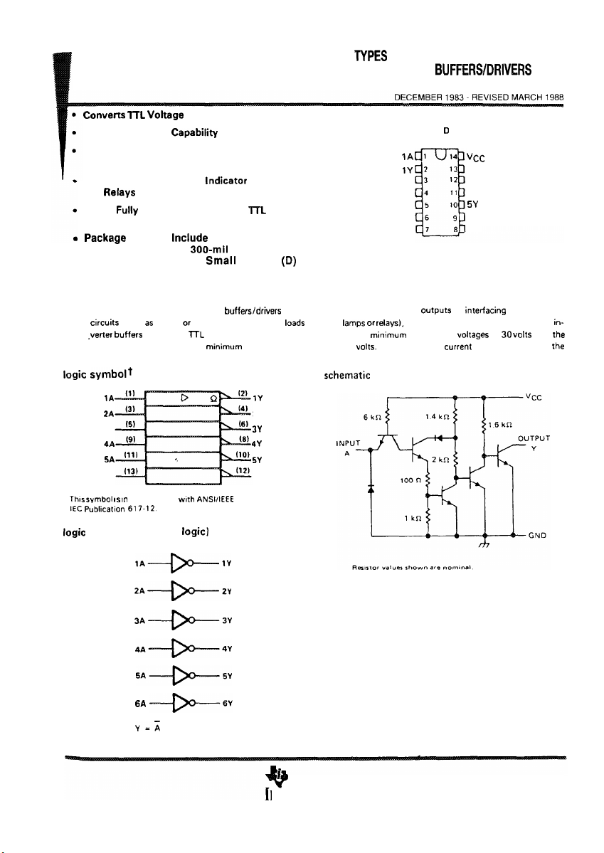
HEX INVERTER
OPEN-COLLECTOR HIGH-VOLTAGE OUTPUTS
Levels to MOS Levels
High Sink-Current
Input Clamping Diodes Simplify System
Design
Open-Collector
and
Inputs
Circuits
(N) and Ceramic (J) 300-mil Dual-In-Line
Packages and Plastic Small Outline
Packages.
description
These monolithic TTL hex inverter buffers/drivers feature high-voltage open-collector
SN5416 and SN7416 have minimum breakdown voltages of 15
SN5406 and SN5416, and 40 milliamperes for the SN7406 and SN7416.
symbolf
3A
Driver for Indicator
Compatible with Most
MOS), or for driving high-current
inputs. The SN5406 and SN7406 have minimum breakdown voltages of 30
Lamps
(such as
2Y
SN7406, SN7416, SN5406, SN5416
SN5406, SN5416 . . . J PACKAGE
SN7406. SN7416 . . .
2A
2Y
3A
3Y
GND
or
and are also characterized for use as
The maximum sink
OR N PACKAGE
(TOP VIEW)
6A
6Y
5A
4A
4Y
for interfacing with high-level
is 30 milliamperes for
‘06, ‘16
WITH
and the
6A
accordance
diagram (positive
6Y
Std 91-1984 and
TEXAS
NSTRUMENTS
3-37
Page 2
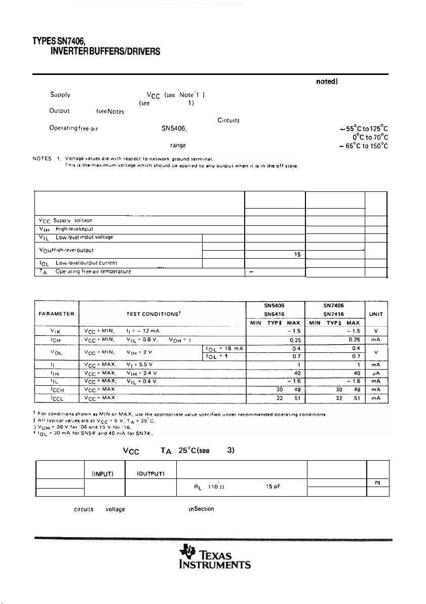
HEX
SN7416, SN5406, SN541 6
WITH
OPEN-COLLECTOR HIGH-VOLTAGE OUTPUTS
absolute maximum ratings over operating free-air temperature range (unless otherwise
voltage,
Input voltage
voltage (sec
Storage temperature
1 and 2): SN5406. SN7406 Circuits
temperature range:
recommended operating conditions
Vollage
High-level Output voltage
electrical characteristics over recommended operating free-air temperature range (unless otherwise noted)
Note
SN5416, SN7416
SN7406. SN7416 Circuits
. . .
. . . . .
SN5416 Circuits
. . . . . . .
‘06 30
‘16
SN5406
SN5416
MIN NOM MAX
4.5
5
2
55 125
MIN NOM MAX
5.5
4.75 5 5.25
2
0.8
30
0 70
. . . . . . . . .
.
. . . . . . . . . .
. . . . . . . . . .
.
. . .
SN7406
SN7416
UNIT
0.8 V
30
15
40
7 v-
5.5 v
30 v
15v
V
V
v
mA
C
switching characteristics, VCC = 5 V,
PARAMETER
‘PLH
‘PHL
NOTE 3: Load
FROM
A
and volrage waveforms are shown
TO
Y
3-38
=
note
TEST CONDITIONS
Section 1
CL=
MIN TYP MAX
10 15
15 23 ns
UNIT
Page 3
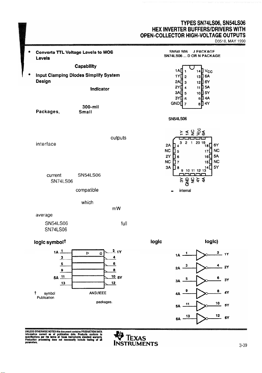
l High Sink-Current Capabillty
l
Open-Collector Driver for Indicator Lamps
and Relays
l Package Options Include Standard Plastic
(N) and Ceramic (J) 300-mil Dual-In-Line
Ceramic Chip Carrier (FK) Package
Plastic Small Outline (D) and
description
These monolithic hex inverter buffers/drivers
feature high-voltage open-collector
MOS), or for driving high-current loads, and
are also characterized for use as inverter
buffers for driving TTL inputs. The ‘LS06 has
a rated output voltage of 30 V. The maximum
sink
for the
These circuits are
for the
it is 40 mA.
is 30 mA and
with most TTL
families. Input are diode-clamped to minimize
transmission-effects,
simplifies design.
Typical power dissipation is 175
and
to
(TOP VIEW)
. . . FK PACKAGE
(TOP VIEW)
NC
No internal connection
The
The
is characterized over the
is characterized for Operation from 0°C to 70°C.
symbolt
2A
3A
4A
6A
This
Pin numbers shown are for D, J, and N packages.
is in accordance with ANSMEEE Std 91-1964 and IEC
military temperature range of -55°C to 125°C.
diagram (positive
2Y
3Y
4Y
6Y
Page 4
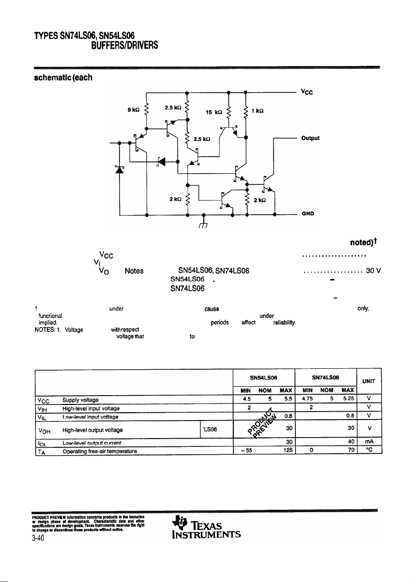
HEX INVERTER BUFFEMDRIVERS WITH
OPEN-COLLECTOR HIGH-VOLTAGE OUTPUTS
gate)
Input
absolute maximum ratings over operating free-air temperature range (unless otherwise
Supply voltage,
Input voltage,
Output voltage,
(see Note 1)
(see
Operating free-air temperature range: SN54LS06 . .
Storage temperature range
Stresses beyond those listed
Exposure to absolute-maximum-rated conditions for extended
2.
This is the maximum voitage
. . . . . . . . . . . . . . . . . . . . . . . . . . . . . . . . . . . . . . . . . . . . . .
. . . . . .
. . . . . . . . . . . . . . . . . . . . . . . . . . . . . . . . . . . . . . . . . . . . . . . . . . . . . . . . . . . . . . .
1 and 2):
. . . . . . . . . . . . . .
. . . . . . . . . . . . . . . . . . . , , , . . , . . . . ,
. . . . . . . . . . . . . . . . . . . . . . . . . . . . . . . . . . . . . . . . . . . . . . . . . . . . . .
“absolute maximum ratings” may
respect to network ground terminal.
should be applied
permanent darnage to the device. This are stress ratings
may affect device
any output when it is in the off state.
‘recommended operating conditions” is not
55°C to 125°C
0°C to 70°C
65°C to 150°C
7v
5.5 v
and
recommended operating conditions
Page 5
HEX
WITH
OPEN-COLLECTOR HIGH-VOLTAGE OUTPUTS
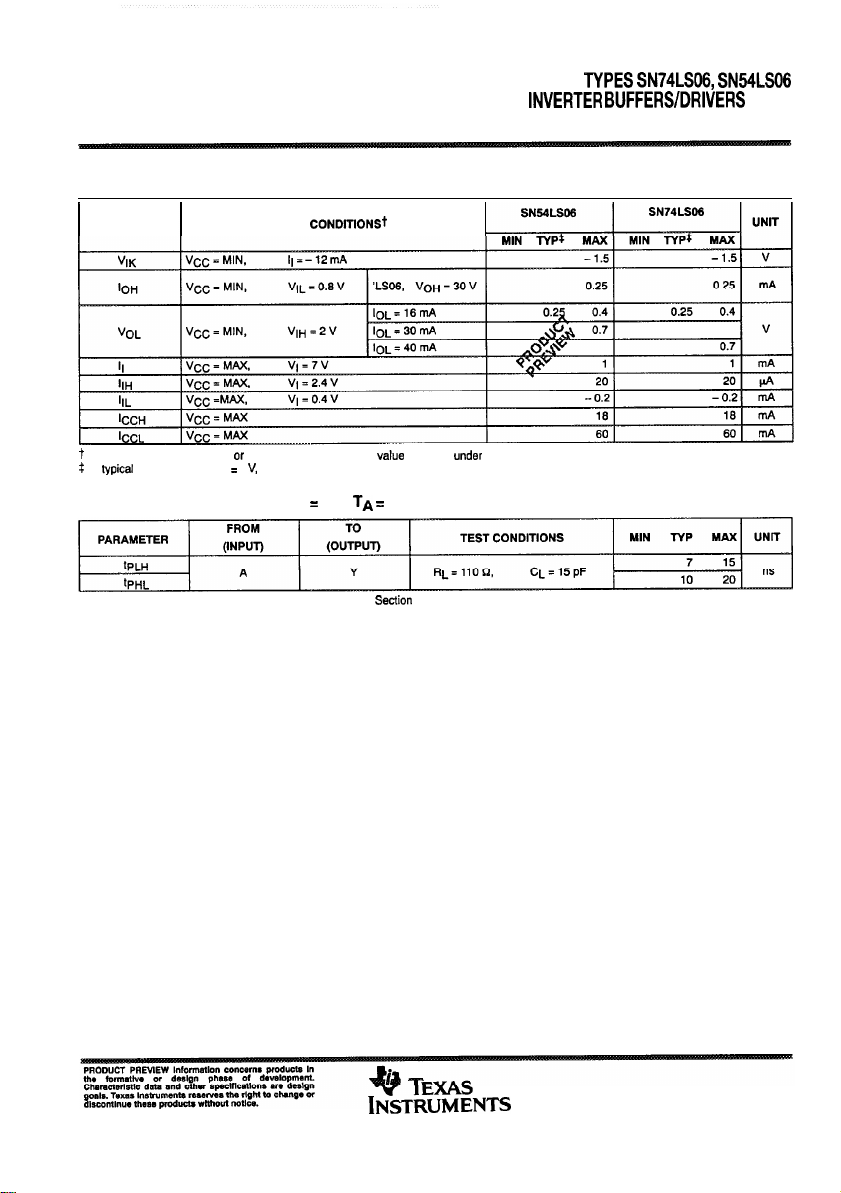
electrical characteristlcs over recommended operating free-alr temperature range (unless
otherwise noted)
PARAMETER
For conditions shown as MIN
All typical values are at VCC
switching characteristics, VCC
NOTE 3: Load circuit and voltage waveforms are shown in Section 1.
TEST CONDITIONSt
MAX, use the appropriate value specified under recommended operating conditions.
5
and TA = 25°C.
5 V, 25°C (see Note 3)
3-41
 Loading...