

Datasheet 74LCXR162245MTD, 74LCXR162245MEX, 74LCXR162245MEA, 74LCXR162245CW Datasheet (Fairchild Semiconductor)
Page 1

August 1998
Revised April 1999
74LCXR162245 Low Voltage 16-Bit Bidirectional Transceiver with 5V Tolerant Inputs/Outputs and 26Ω Series
Resistors in the Outputs
© 1999 Fairchild Semiconductor Corporation DS500052.prf www.fairchildsemi.com
74LCXR162245
Low Voltage 16-Bit Bidirectional Transceiver with 5V
Tolerant Inputs/Outputs and 26Ω Series Resistors in the
Outputs
General Description
The LCXR162245 contains sixteen non-inverting bidire ctional buffers with 3-STATE outputs and is intended for bus
oriented application s. The device is de signed for low vo ltage (2.5V or 3.3V) V
CC
applications with capability of inter-
facing to a 5V signal environment. The device is byte
controlled. Each byte has separate control inputs which
could be shorted toge ther fo r ful l 16-bi t op eration . The T /R
inputs determine the direction of data flow through the
device. The OE
inputs disable bo th the A and B ports by
placing them in a high impedance state.
In addition, all A and B outputs include equivalent 26Ω
(nominal) series resistor s to reduce overshoot and undershoot and are designed to sink/source up to 12 mA at
V
CC
= 3.0V.
The LCXR162245 is fa bricated with an advanced CMOS
technology to achieve high speed operation while maintaining CMOS low power dissipation.
Features
■ 5V tolerant inputs and outputs
■ 2.3V–3.6V V
CC
specifications provided
■ A and B side outputs have equivalent 26Ω series
resistors
■ 5.3 ns t
PD
max (VCC = 3.3V), 20 µA ICC max
■ Power down high impedance inputs and outputs
■ Supports live insertion/withdrawal (Note 1)
■ Flow through pinout
■ Implements patented noise/EMI reduction circuitry
■ Latch-up performance exceeds 500 mA
■ ESD performance:
Human body model > 2000V
Machine model > 200V
Note 1: To ensure the high-impedance state d uring pow er up or d own OE
should be tied to VCC through a pull-up res istor: the m inimu m value or t he
resistor is determin ed by the current-sourcing capability of the dr iv er.
Ordering Code:
Devices also availab le in Tape and Reel. Specify by appending th e s uffix let t er “x ” to the ordering code.
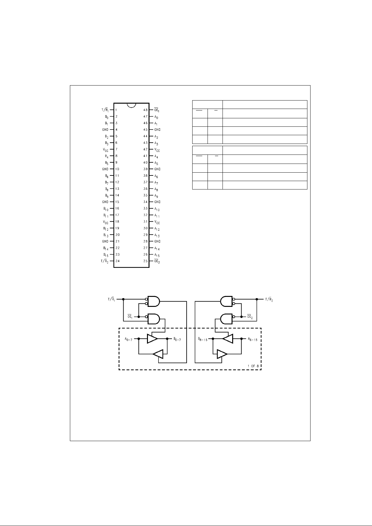
Logic Symbol Pin Descriptions
Order Number Package Number Package Description
74LCXR162245MEA MS48A 48-Lead Small Shrink Outline Package (SSOP), JEDEC MO-118, 0.300” Wide
74LCXR162245MTD MTD48 48-Lead Thin Shrink Small Outline Package (TSSOP), JEDEC MO-153, 6.1mm Wide
Pin Names Description
OE
n
Output Enable Input
T/R
n
Transmit/Receive Input
A
0–A15
Side A Inputs or 3-STATE Outputs
B
0–B15
Side B Inputs or 3-STATE Outputs
Page 2
www.fairchildsemi.com 2
74LCXR162245
Connection Diagram Tr uth Tables
Note 2: A and B port inputs are still activ e
Logic Diagram
Inputs Outputs
OE
1
T/R
1
L L Bus B0–B7 Data to Bus A0–A
7
L H Bus A0–A7 Data to Bus B0–B
7
H X HIGH Z State on A0–A7, B0–B7 (Note 2)
Inputs Outputs
OE
2
T/R
2
L L Bus B8–B15 Data to Bus A8–A
15
L H Bus A8–A15 Data to Bus B8–B
15
H X HIGH Z State on A8–A15, B8–B
15
(Note 2)
Page 3
3 www.fairchildsemi.com
74LCXR162245
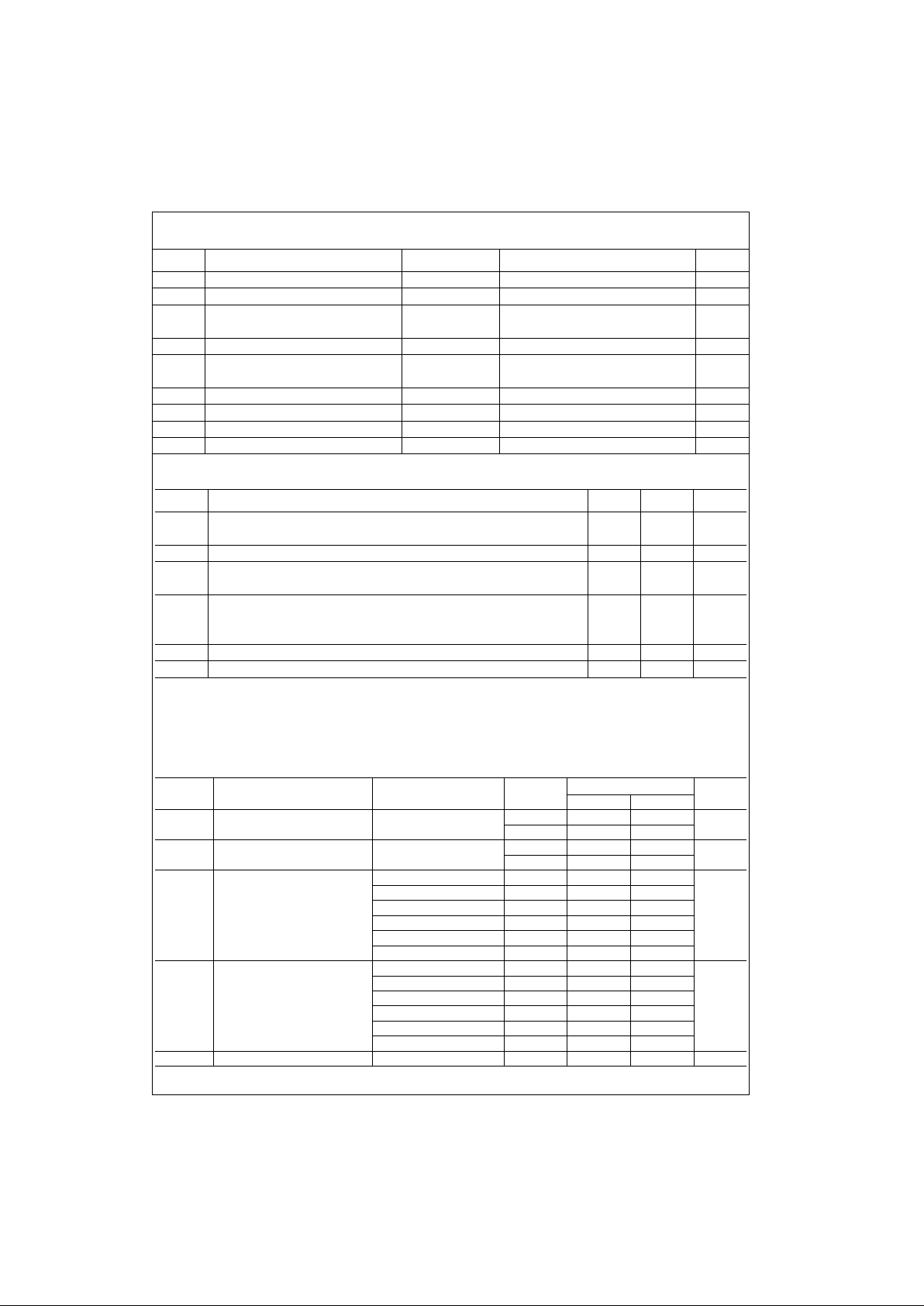
Absolute Maximum Ratings(Note 3)
Recommended Operating Conditions (Note 5)
Note 3: The Absolute Maximum Ratings are those values beyond which the safety of the device cannot be guaranteed. The device should not be operated
at these limits. The parametric values defined in the Electrical Characteristics tables are not guaranteed at the Absolute Maximum Ratings. The “Recommended Operating C onditions” table will def ine the conditions for act ual device operation.
Note 4: I
O
Absolute Maximum Rating must be observed.
Note 5: Unused pins (Inputs or I/O's) must be held HIGH or LOW. They may not Float.
DC Electrical Characteristics
Symbol Parameter Value Conditions Units
V
CC
Supply Voltage −0.5 to +7.0 V
V
I
DC Input Voltage −0.5 to +7.0 V
V
O
DC Output Voltage −0.5 to +7.0 Output in 3-STATE
V
−0.5 to V
CC
+ 0.5 Output in HIGH or LOW State (Note 4)
I
IK
DC Input Diode Current −50 VI < GND mA
I
OK
DC Output Diode Current −50 VO < GND
mA
+50 V
O
> V
CC
I
O
DC Output Source/Sink Current ±50 mA
I
CC
DC Supply Current per Supply Pin ±100 mA
I
GND
DC Ground Cu rrent per Ground Pin ±100 mA
T
STG
Storage Temperature −65 to +150 °C
Symbol Parameter Min Max Units
V
CC
Supply Voltage Operating 2.0 3.6
V
Data Retention 1.5 3.6
V
I
Input Voltage 0 5.5 V
V
O
Output Voltage HIGH or LOW State 0 V
CC
V
3-STATE 0 5.5
I
OH/IOL
Output Current VCC = 3.0V − 3.6V ±12
mA V
CC
= 2.7V − 3.0V ±8
V
CC
= 2.3V − 2.7V ±4
T
A
Free-Air Operating Temperature −40 85 °C
∆t/∆V Input Edge Rate, V
IN
= 0.8V–2.0V, VCC = 3.0V 0 10 ns/V
Symbol Parameter Conditions
VCC
(V)
TA = −40°C to +85°C
Units
Min Max
V
IH
HIGH Level Input Voltage 2.3 − 2.7 1.7
V
2.7 − 3.6 2.0
V
IL
LOW Level Input Voltage 2.3 − 2.7 0.7
V
2.7 − 3.6 0.8
V
OH
HIGH Level Output Voltage IOH = −100 µA 2.3 − 3.6 VCC − 0.2
V
IOH = −4 mA 2.3 1.8
IOH = −4 mA 2.7 2.2
IOH = −6 mA 3.0 2.4
IOH = −8 mA 2.7 2.0
IOH = −12 mA 3.0 2.0
V
OL
LOW Level Output Voltage IOL = 100 µA 2.3 − 3.6 0.2
V
IOL = 4 mA 2.3 0.6
IOL = 4 mA 2.7 0.4
IOL = 6 mA 3.0 0.55
IOL = 8 mA 2.7 0.6
IOL = 12 mA 3.0 0.8
I
I
Input Leakage Current 0 ≤ VI ≤ 5.5V 2.3 − 3.6 ±5.0 µA
Page 4

www.fairchildsemi.com 4
74LCXR162245
DC Electrical Characteristics (Continued)
Note 6: Outputs dis abled or 3-STATE only.
AC Electrical Characteristics
Note 7: Skew is defined as t he absolute value of t he difference betwee n t he actual propagat ion delay for any tw o separate outpu ts of the same device. T he
specification applies to any outputs switching in the same direction, either HIGH-to-LOW (t
OSHL
) or LOW-to-HIGH (t
OSLH
). Parameter guaranteed by design.
Dynamic Switching Characteristics
Capacitance
Symbol Parameter Conditions
VCC
(V)
TA = −40°C to +85°C
Units
Min Max
I
OZ
3-STATE I/O Leakage 0 ≤ VO ≤ 5.5V 2.3 − 3.6 ±5.0
µA
VI = VIH or V
IL
I
OFF
Power-Off Leakage Current VI or VO = 5.5V 0 10 µA
I
CC
Quiescent Supply Current VI = VCC or GND 2.3 − 3.6 20
µA
3.6V ≤ VI, VO ≤ 5.5V (Note 6) 2.3 − 3.6 ±20
∆I
CC
Increase in ICC per Input VIH = VCC −0.6V 2.3 − 3.6 500 µA
Symbol Parameter
TA = −40°C to +85°C, RL = 500Ω
Units
VCC = 3.3V ± 0.3V VCC = 2.7V VCC = 2.5V ± 0.2
CL = 50 pF CL = 50 pF CL = 30 pF
Min Max Min Max Min Max
t
PHL
Propagation Delay 1.5 5.3 1.5 6.0 1.5 6.4
ns
t
PLH
An to Bn or Bn to A
n
1.5 5.3 1.5 6.01.5 6.4
t
PZL
Output Enable Time 1.5 7.3 1.5 8.0 1.5 9.5
ns
t
PZH
1.5 7.3 1.5 8.01.5 9.5
t
PLZ
Output Disable Time 1.5 6.4 1.5 6.9 1.5 7.7
ns
t
PHZ
1.5 6.4 1.5 6.9 1.5 7.7
t
OSHL
Output to Output Skew (Note 7) 1.0
ns
t
OSLH
1.0
Symbol Parameter Conditions
V
CC
(V)
TA = 25°C
Units
Typical
V
OLP
Quiet Output Dynamic Peak V
OL
CL = 50 pF, VIH = 3.3V, VIL = 0V 3.3 0.35
V
CL = 30 pF, VIH = 2.5V, VIL = 0V 2.5 0.25
V
OLV
Quiet Output Dynamic Valley V
OL
CL = 50 pF, VIH = 3.3V, VIL = 0V 3.3 −0.35
V
CL = 30 pF, VIH = 2.5V, VIL = 0V 2.5 −0.25
Symbol Parameter Conditions Typical Units
C
IN
Input Capacitance VCC = Open, VI = 0V or V
CC
7 pF
C
I/O
Input/Output Capacitance VCC = 3.3V, VI = 0V or V
CC
8 pF
C
PD
Power Dissipation Capacitance VCC = 3.3V, VI = 0V or VCC, f = 10 MHz 20 pF
Page 5

5 www.fairchildsemi.com
74LCXR162245
AC LOADING and WAVEFORMS Generic for LCX Family
FIGURE 1. AC Test Circuit (C
L
includes probe and jig capacitance)
Waveform for Inverting and Non-Inverting Functions
Propagation Delay. Pulse Width and t
rec
Waveforms
3-STATE Output Low Enable and
Disable Times for Logic
3-STATE Output High Enable and
Disable Times for Logic
Setup Time, Hold Time and Recovery Time for Logic
t
rise
and t
fall
FIGURE 2. Waveforms
(Input Characteristics; f =1MHz, t
R
= tF = 3ns)
Test Switch
t
PLH
, t
PHL
Open
t
PZL
, t
PLZ
6V at VCC = 3.3 ± 0.3V
V
CC
x 2 at VCC = 2.5 ± 0.2V
t
PZH,tPHZ
GND
Symbol
V
CC
3.3V ± 0.3V 2.7V 2.5V ± 0.2V
V
mi
1.5V 1.5V VCC/2
V
mo
1.5V 1.5V VCC/2
V
x
VOL + 0.3V VOL + 0.3V VOL + 0.15V
V
y
VOH − 0.3V VOH − 0.3V VOH − 0.15V
Page 6

www.fairchildsemi.com 6
74LCXR162245
Schematic Diagram Generic for LCX Family
Page 7

7 www.fairchildsemi.com
74LCXR162245
Physical Dimensions inches (millimeters) unless otherwise noted
48-Lead Small Shrink Outline Package (SSOP), JEDEC MO-118, 0.300” Wide
Package Number MS48A
Page 8

Fairchild does not assume any responsibility for use of any circuitry described, no circuit patent licenses are implied and Fairchild reserves the right at any time without notice to change said circuitry and specifications.
74LCXR162245 Low Voltage 16-Bit Bidirectional Transceiver with 5V Tolerant Inputs/Outputs and 26Ω Series
Resistors in the Outputs
LIFE SUPPORT POLICY
FAIRCHILD’S PRODUCTS ARE NOT AUTHORIZED FOR USE AS CRITICAL COMPONENTS IN LIFE SUPPORT
DEVICES OR SYSTEMS WITHOUT THE EXPRESS WRITTEN APPROVAL OF THE PRESIDENT OF FAIRCHILD
SEMICONDUCTOR CORPORATION. As used herein:
1. Life support devices or systems are devices or syste ms
which, (a) are intended for surgical implant into the
body, or (b) support or sustain life, and (c) whose failure
to perform when properly used in accordance with
instructions for use provided in the labeling, can be reasonably expected to result in a significant inju ry to the
user.
2. A critical component i n any compon ent of a lif e support
device or system whose failu re to perform can be reasonably expected to ca use the fa i lure of the life su pp ort
device or system, or to affect its safety or effectiveness.
www.fairchildsemi.com
Physical Dimensions inches (millimeters) unless otherwise noted (Continued)
48-Lead Thin Shrink Small Outline Package (TSSOP), JEDEC MO-153, 6.1mm Wide
Package Number MTD48
 Loading...