

Page 1
1/10June 2002
■ 5V TOLERANT INPUTS AND OUTPUTS
■ HIGH SPEED :
t
PD
= 6.0 ns (MAX.) at VCC = 3V
■ POWER DOWN PROTECTION ON INPUT S
AND OUTPUTS
■ SYMMETRICAL OUTPUT IMPEDANCE:
|I
OH
| = IOL = 24mA (MIN) at VCC = 3V
■ PCI BUS LEVELS GUARANT EED AT 2 4 mA
■ BALANCED PROPAGATION DELAYS:
t
PLH
≅ t
PHL
■ OPERATING VOLTAGE RANGE:
V
CC
(OPR) = 2.0V to 3.6V (1.5V Data
Retention)
■ PIN AND FUNCTION COMPATIBLE WITH
74 SERIES 257
■ LATCH-UP PERFORMANCE EXCEEDS
500mA (JESD 17)
■ ESD PERFORMANCE:
HBM > 2000V (MIL STD 883 method 3015);
MM > 200V
DESCRIPTION
The 74LCX257 is a low v oltage CMOS QUAD 2
CHANNEL MULTIPLEXER (3-STATE) fabricated
with sub-micron silicon gate and double-layer
metal wiring C
2
MOS technology. It is ideal for low
power and high speed 3.3V applications; it can be
interfaced to 5V signal environment for both inputs
and ou tputs.
It is composed of four independent 2 channel
multiplexers with commo n SELECT and ENABLE
(OE
) INPUT. The 74LCX257 is a non-inverting
multiplexer. When the ENABLE INPUT is held
"High", all outputs become in high impedance
state. If SELECT INPUT is held "L ow", "A" dat a is
selected, when SELECT INPUT is "High", "B"
data is chosen.
It has same speed performance at 3. 3V than 5V
AC/ACT family, combined with a lower power
consumption.
All inputs and outputs are equipped with
protection circuits against stat ic discharge, giving
them 2KV ESD immunity and transient excess
voltage.
74LCX257
LOW VOLTAGE CMOS QUAD 2 CHANNEL MULTIPLEXER
WITH 5V TOLERANT IN PU TS AN D OU TPUTS (3-STATE)
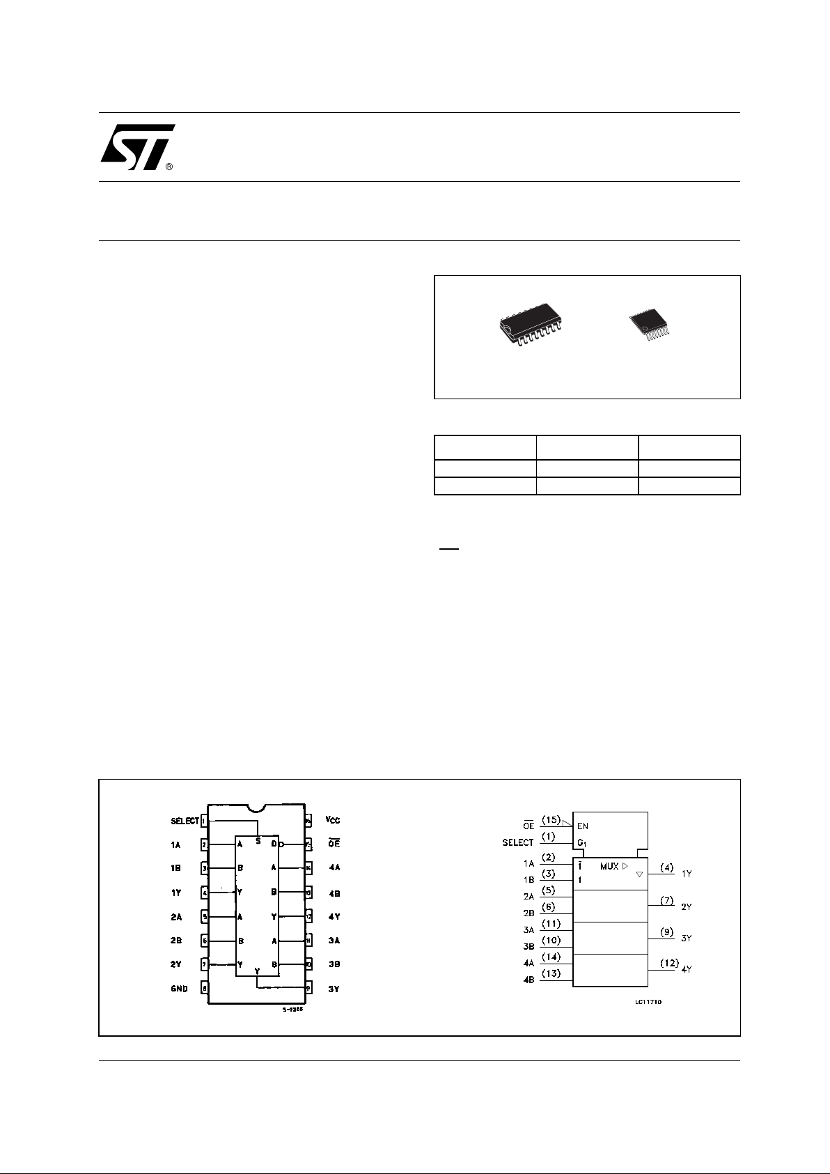
PIN CONNECTION AND IEC LOGIC SYMBOLS
ORDER CODES
PACKAGE TUBE T & R
SOP 74LCX257M 74LCX257MTR
TSSOP 74LCX257TTR
TSSOPSOP
Page 2

74LCX257
2/10
INPUT AND OUTPUT EQUIVALENT CIRCUIT
PIN DESCRIPTION
TRUTH TABLE
X : Don’t Care
Z : High Impedance
PIN No SYMBOL NAME AND FUNCTION
1 SELECT Common Data Select Inputs
2, 5, 11, 14 1A to 4A Data Inputs From Source A
3, 6, 10, 13 1B to 4B Data Inputs From Source B
4, 7, 9, 12 1Y to 4Y 3 State Multiplexer Outputs
15 OE
3 State Output Enable Inputs (Active
LOW)
8 GND Ground (0V)
16 V
CC
Positive Supply Voltage
INPUTS OUTPUT
OE
SELECT A B Y
HXXXZ
LLLXL
LLHXH
LHXLL
LHXHH
Page 3

74LCX257
3/10
LOGIC DIAGRAM
This log i c diagram has not be used to esti m ate propaga tion delays
ABSOLUTE MAXIMUM RATINGS
Absolute Maximum Ratings are those values beyond which damage to the device may occur. Functional operation under these conditions is
not implied
1) I
O
absolute ma xim um rating mu st be observed
2) V
O
< GND
Symbol Parameter Value Unit
V
CC
Supply Voltage
-0.5 to +7.0 V
V
I
DC Input Voltage
-0.5 to +7.0 V
V
O
DC Output Voltage (OFF State)
-0.5 to +7.0 V
V
O
DC Output Voltage (High or Low State) (note 1) -0.5 to VCC + 0.5
V
I
IK
DC Input Diode Current
- 50 mA
I
OK
DC Output Diode Current (note 2)
- 50 mA
I
O
DC Output Current
±
50 mA
I
CC
DC Supply Current per Supply Pin
±
100 mA
I
GND
DC Ground Current per Supply Pin
±
100 mA
T
stg
Storage Temperature
-65 to +150 °C
T
L
Lead Temperature (10 sec)
300 °C
Page 4

74LCX257
4/10
RECOMMENDED OPERATING CONDITIONS
1) Truth T abl e guaranteed: 1.5V to 3.6V
2) V
IN
from 0.8V to 2V at VCC = 3.0V
DC SPECIFICATIONS
Symbol Parameter Value Unit
V
CC
Supply Voltage (note 1)
2.0 to 3.6 V
V
I
Input Voltage
0 to 5.5 V
V
O
Output Voltage (OFF State)
0 to 5.5 V
V
O
Output Voltage (High or Low State) 0 to V
CC
V
I
OH
, I
OL
High or Low Level Output Current (VCC = 3.0 to 3.6V)
±
24 mA
I
OH
, I
OL
High or Low Level Output Current (VCC = 2.7V)
±
12 mA
T
op
Operating Temperature
-55 to 125 °C
dt/dv Input Rise and Fall Time (note 2) 0 to 10 ns/V
Symbol Parameter
Test Condition Value
Unit
V
CC
(V)
-40 to 85 °C -55 to 125 °C
Min. Max. Min. Max.
V
IH
High Level Input
Voltage
2.7 to 3.6
2.0 2.0 V
V
IL
Low Level Input
Voltage
0.8 0.8 V
V
OH
High Level Output
Voltage
2.7 to 3.6
IO=-100 µAVCC-0.2 VCC-0.2
V
2.7
I
O
=-12 mA
2.2 2.2
3.0
I
O
=-18 mA
2.4 2.4
I
O
=-24 mA
2.2 2.2
V
OL
Low Level Output
Voltage
2.7 to 3.6
I
O
=100 µA
0.2 0.2
V
2.7
I
O
=12 mA
0.4 0.4
3.0
I
O
=16 mA
0.4 0.4
I
O
=24 mA
0.55 0.55
I
I
Input Leakage
Current
2.7 to 3.6
V
I
= 0 to 5.5V
±
5
±
5
µ
A
I
off
Power Off Leakage
Current
0
V
I
or VO = 5.5V
10 10
µ
A
I
OZ
High Impedance
Output Leakage
Current
2.7 to 3.6
V
I
= VIH or V
IL
VO = 0 to V
CC
±
5
±
5
µ
A
I
CC
Quiescent Supply
Current
2.7 to 3.6
VI = VCC or GND
10 10
µ
A
V
I
or VO= 3.6 to 5.5V
±
10
±
10
∆
I
CC
ICC incr. per Input
2.7 to 3.6
VIH = VCC - 0.6V
500 500
µ
A
Page 5

74LCX257
5/10
DYNAMIC SWITCHING CHARACTERISTICS
1) Number of outputs d ef i ned as "n". Me asured with "n-1" output s switching from HIGH to LO W or LOW to HIGH. The remaini ng outpu t is
measur ed i n the LOW state.
AC ELECTRICAL CHARACTERISTICS
1) Skew is defined as the absolute value of the difference between the actual propagation delay for any two outputs of the same device switching in the same direction, either HIGH or LOW (t
OSLH
= | t
PLHm
- t
PLHn
|, t
OSHL
= | t
PHLm
- t
PHLn
|)
2) Param eter guaran te ed by design
CAPACITIVE CHARACTERISTICS
1) CPD is defined as the value of the IC’s internal equivalent capacitance which is calculated from the operating current consumption without
load. (R ef er to Test Circui t). Averag e operating cu rrent can be obtained by the foll owing equat io n. I
CC(opr)
= CPD x VCC x fIN + ICC/4 (per
channel)
Symbol Parameter
Test Condition Value
Unit
V
CC
(V)
T
A
= 25 °C
Min. Typ. Max.
V
OLP
Dynamic Low Level Quiet
Output (note 1)
3.3
C
L
= 50pF
V
IL
= 0V, VIH = 3.3V
0.8
V
V
OLV
-0.8
Symbol Parameter
Test Condition Value
Unit
V
CC
(V)
C
L
(pF)
R
L
(Ω)
t
s
= t
r
(ns)
-40 to 85 °C -55 to 125 °C
Min. Max. Min. Max.
t
PLH tPHL
Propagation Delay
Time (A, B to Y)
2.7
50 500 2.5
1.5 6.5 1.5 6.5
ns
3.0 to 3.6 1.5 6.0 1.5 6.0
t
PLH tPHL
Propagation Delay
Time (SELECT to Y)
2.7
50 500 2.5
1.5 8.5 1.5 8.5
ns
3.0 to 3.6 1.5 7.0 1.5 7.0
t
PZL tPZH
Output EnableTime 2.7
50 500 2.5
1.5 8.5 1.5 8.5
ns
3.0 to 3.6 1.5 7.0 1.5 7.0
t
PLZ tPHZ
Output DisableTime 2.7
50 500 2.5
1.5 6.0 1.5 6.0
ns
3.0 to 3.6 1.5 5.5 1.5 5.5
t
OSLH
t
OSHL
Output To Output
Skew Time (note1,
2)
3.0 to 3.6 50 500 2.5 1.0 1.0 ns
Symbol Parameter
Test Condition Value
Unit
V
CC
(V)
T
A
= 25 °C
Min. Typ. Max.
C
IN
Input Capacitance
3.3
VIN = 0 to V
CC
7pF
C
OUT
Output Capacitance
3.3
VIN = 0 to V
CC
8pF
C
PD
Power Dissipation Capacitance
(note 1)
3.3 fIN = 10MHz
V
IN
= 0 or V
CC
25
pF
Page 6

74LCX257
6/10
TEST CIRCUIT
CL = 50 pF or equival ent (includes jig and probe capacitance)
R
L
= R1 = 500Ω or equivalent
R
T
= Z
OUT
of pulse generator (typically 50Ω)
WAVEFORM 1 : PROPAGATION DELAYS (f=1MHz; 50% duty cycle)
TEST SWITCH
t
PLH
, t
PHL
Open
t
PZL
, t
PLZ
6V
t
PZH
, t
PHZ
GND
Page 7

74LCX257
7/10
WAVEFORM 2 : OUTPUT ENABLE AND DISABLE TIME (f=1MHz; 50 % duty cycl e )
Page 8

74LCX257
8/10
DIM.
mm. inch
MIN. TYP MAX. MIN. TYP. MAX.
A 1.75 0.068
a1 0.1 0.2 0.003 0.007
a2 1.65 0.064
b 0.35 0.46 0.013 0.018
b1 0.19 0.25 0.007 0.010
C 0.5 0.019
c1 45° (typ.)
D 9.8 10 0.385 0.393
E 5.8 6.2 0.228 0.244
e 1.27 0.050
e3 8.89 0.350
F 3.8 4.0 0.149 0.157
G 4.6 5.3 0.181 0.208
L 0.5 1.27 0.019 0.050
M 0.62 0.024
S8° (max.)
SO-16 MECHANICAL DATA
PO13H
Page 9

74LCX257
9/10
DIM.
mm. inch
MIN. TYP MAX. MIN. TYP. MAX.
A 1.2 0.047
A1 0.05 0.15 0.002 0.004 0.006
A2 0.8 1 1.05 0.031 0.039 0.041
b 0.19 0.30 0.007 0.012
c 0.09 0.20 0.004 0.0089
D 4.9 5 5.1 0.193 0.197 0.201
E 6.2 6.4 6.6 0.244 0.252 0.260
E1 4.3 4.4 4.48 0.169 0.173 0.176
e 0.65 BSC 0.0256 BSC
K0° 8°0° 8°
L 0.45 0.60 0.75 0.018 0.024 0.030
TSSOP16 MECHANICAL DATA
c
E
b
A2
A
E1
D
1
PIN 1 IDENTIFICATION
A1
L
K
e
0080338D
Page 10

74LCX257
10/10
Information furnished is believed to be accurate and reliable. However, STMicroelectronics assumes no responsibilit y for the
consequences of use of such informatio n nor for any infringement of paten ts or o ther rig hts of t hird part ies which ma y result from
its use. No license is granted by implication or otherwise under any patent or patent rights of STMicroelectronics. Specifications
mentioned in this publication are subject to change without notice. This publication supersedes and replaces all information
previousl y suppl ied. STM icroel ectronics produc ts are not auth orized for use as c ritica l compone nts in l ife s upport dev ices or
systems without express written approval of STMicroelectronics.
© The ST logo is a registered trademark of STMicroelectronics
© 2002 STMicroelectronics - Printed in Italy - All Rights Reserved
STMicroelectronics GROUP OF COMPANIES
Australia - Brazil - Canada - China - Finland - France - Germany - Hong Kong - India - Israel - Italy - Japan - Malaysia - Malta - Morocco
Singapore - Spain - Sweden - Switzerland - United Kingdom - United States.
© http://www.st.com
 Loading...