

Page 1
查询74LCX16240A供应商
74LCX16240A
LOWVOL T AGECMOS16- BI TBUSBUFFER(3-STA TEINV.)
WITH5VTOLERANT INPUTSAND OUTPUTS
■ 5VTOLERANTINPUTSANDOUTPUTS
■
HIGH SPEED:
t
=4.9ns(MAX.)at VCC=3.0V
PD
■
POWER-DOWNPROTECTIONONINPUTS
ANDOUTPUTS
■ SYMMETRICAL OUTPUTIMPEDANCE:
|=IOL=24mA (MIN)
|I
OH
■ PCIBUSLEVELSGUARANTEED AT 24mA
■ BALANCEDPROPAGATIONDELAYS:
t
≅ t
PLH
PHL
■ OPERATINGVOLTAGERANGE:
(OPR)= 2.7Vto 3.6V (1.5VDataRetention)
V
CC
■ PINANDFUNCTIONCOMPATIBLEWITH
74SERIES16240
■ LATCH-UPPERFORMANCE EXCEEDS500mA
■ ESDPERFORMANCE:
HBM>2000V;MM > 200V
(TSSOP48Package)
ORDERCODES :
74LCX16240AT
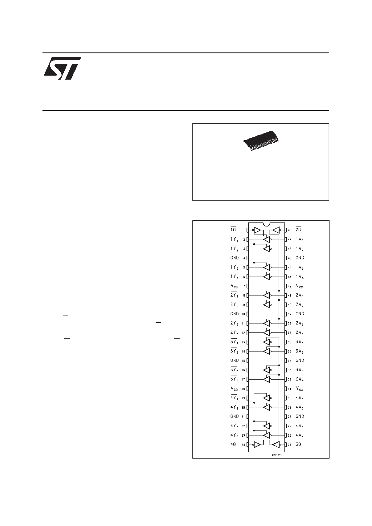
PIN CONNECTION
T
DESCRIPTION
The LCX16240A is a low voltage CMOS 16-BIT
BUS BUFFER fabricated with sub-micron silicon
gate and double-layer metal wiring C
2
MOS
technology. It is ideal for low power and high
speed 3.3V applications; it can be interfaced to
5V signal environment for both inputs and
outputs.
Any nG output control governs four BUS
BUFFERS. Output Enable input (nG) tied
togethergives full 16-bitoperation.
When nG is LOW, the outputs are on. When nG
is HIGH,the output are in highimpedancestate.
This device is designed to be used with 3 state
memoryaddress drivers, etc.
It has better speed performance at 3.3V than 5V
LSTTL family combined with the true CMOS low
powerconsumption.
All inputs and outputs are equipped with
protection circuits against static discharge, giving
them 2KV ESD immunity and transient excess
voltage.
February 1999
1/8
Page 2
74LCX16240A
INPUT AND OUTPUT EQUIVALENTCIRCUIT
PI N No SYM BO L NAM E AND FUNCTIO N
1 1G Output Enable Input
2,3,5,6 1Y1to 1Y4 Data Outputs
8,9,11,12 2Y1to 2Y4 Data Outputs
13,14, 16,17 3Y1to 3Y4 Data Outputs
19,20, 22,23 4Y1to 4Y4 Data Outputs
24 4G Output Enable Input
25 3G Output Enable Input
30,29, 27,26 4A1to 4A4 Data Inputs
36,35, 33,32 3A1to 3A4 Data Inputs
41,40, 38,37 2A1to 2A4 Data Inputs
47,46, 44,43 1A1to 1A4 Data Inputs
48 2G Output Enable Input
4,10,15,21,
28,34, 39,45
7,18,31,42 V
GND Ground (0V)
Positive Supply Voltage
CC
IEC LOGIC SYMBOLSPIN DESCRIPTION
TRUTH TABLE
INPUT OUTPU T
GAnYn
LLH
LHL
HXZ
X:”H” or”L”
Z:Highimpedance
2/8
Page 3
74LCX16240A
ABSOLUTE MAXIMUM RATINGS
Symb o l Para met er Val u e Uni t
V
V
V
V
I
I
OK
I
orI
I
CC
T
T
AbsoluteMaximumRatingsarethose valuesbeyond whichdamagetothedevicemayoccur. Functionaloperationunder these conditionisnotimplied.
1)I
absolutemaximumratingmustbeobserved
O
2)V
<GND, VO>V
O
RECOMMENDED OPERATING CONDITIONS
Symb o l Pa rameter Va l u e U n i t
V
V
V
I
OH,IOL
I
OH,IOL
T
dt/dv Input Transition Rise or Fall Rate (V
1)TruthTableguaranteed: 1.5V to3.6V
2)V
from0.8Vto 2.0V
IN
Supply Voltage -0.5to+ 7.0 V
CC
DC Input Voltage -0.5to+ 7.0 V
I
DC Output Voltage (OFF state) -0.5to+ 7.0 V
O
DC Output Voltage (High or Low State) (note1) -0.5toVCC+0.5 V
O
DC Input Diode Current -50 mA
IK
DC Output Diode Current (note2)
DC Output Source/Sink Current
O
DC VCCor Ground Current Per Supply Pin ±100 mA
GND
Storage Temperature -65to+150
stg
Lead Temperature (10 sec) 300
L
CC
Supply Voltage (note 1) 2.0to3.6 V
CC
V
Input Voltage 0to5.5 V
I
Output Voltage (OFF state) 0to5.5 V
O
Output Voltage (High or Low State) 0toV
O
50 mA
±
50 mA
±
CC
High or Low Level Output Current (VCC= 3.0 to 3.6V) ±24 mA
High or Low Level Output Current (VCC= 2.7 to 3.0V)
Operating Temperature: -40to+85
op
= 3.0V) (note 2) 0to10 ns/V
CC
12 mA
±
o
C
o
C
V
o
C
3/8
Page 4

74LCX16240A
DC SPECIFICATIONS
Symb o l Parameter Test Co n d iti on s Val ue Uni t
V
CC
(V)
High Level Input Voltage
V
IH
Low Level Input Voltage 0.8 V
V
IL
High Level Output Voltage 2.7to3.6
V
OH
Low Level Output Voltage 2.7to3.6
V
OL
Input Leakage Current
I
I
3 State Output Leakage Current 2.7to3.6 VI=VIHorV
I
OZ
2.7to 3.6
V
2.7 I
I=VIH
orV
3.0
V
2.7 I
3.0 I
I=VIH
orV
3.0 I
2.7to 3.6
IO=-100 µAVCC-0.2
=-12mA 2.2
O
IL
=-18mA 2.4
I
O
=-24mA 2.2
I
O
IO=100µA0.2
=12mA 0.4
O
IL
=16mA 0.4
O
=24mA 0.55
O
VI=0 to5.5V ±5 µA
IL
-40 to85
Min. Max.
2.0
o
C
V
V
V
±5 µA
VO=0to5.5V
Power Off Leakage Current 0 VIorVO=5.5V(perpin) 10 µA
I
off
Quiescent Supply Current 2.7to3.6 VI=VCCorGND 20
I
CC
V
I
orVO=
20
±
µA
3.6to5.5V
ICC incr. per input 2.7to3.6 VIH=VCC-0.6V 500 µA
∆I
CC
DYNAMICSWITCHING CHARACTERISTICS
Symbol Parameter Test Condit ions Value Un it
T
V
CC
(V)
V
V
1)Numberofoutputsdefinedas”n”.Measured with”n-1”outputs switchingfromHIGHtoLOWor LOWtoHIGH.Theremainingoutputismeasured in
theLOWstate.
Dynamic Low Voltage Quiet Output
OLP
(note 1)
OLV
3.3 CL=50pF
V
=0V
IL
V
=3.3V
IH
Min. Typ. Max.
=25oC
A
0.8
-0.8
V
4/8
Page 5

AC ELECTRICAL CHARACTERISTICS (CL= 50 pF, RL= 500 Ω, Input tr=tf= 2.5ns)
74LCX16240A
Symbol Parameter Test Condit ion Value Unit
V
CC
(V)
t
Propagation Delay Time 2.7
PLH
t
PHL
t
Output Enable Time 2.7
PZL
t
PZH
t
Output Disable Time 2.7
PLZ
t
PHZ
t
t
1) Skew isdefinedastheabsolute value ofthedifferencebetween theactualpropagation delayfor anytwooutputsofthesamedeviceswitchinginthe
samedirection, eitherHIGHor LOW(t
2) Parameterguaranteed bydesign
Output to Output Skew Time (note 1, 2) 3.0to3.6 1.0 ns
OSLH
OSHL
OSLH
=|t
PLHm-tPLHn
|,t
=|t
OSHL
3.0to3.6 1.5 4.9
3.0to3.6 1.5 6.5
3.0to3.6 1.5 5.5
PHLm-tpHLn
|)
Waveform -40 t o 85
Mi n . Max.
1
2
2
1.5 5.9
1.5 7.5
1.5 6.5
o
C
ns
ns
ns
CAPACITIVE CHARACTERISTICS
Symbol Parameter Test Condi tions Value Unit
V
CC
(V)
Input Capacitance
C
IN
C
1)CPDisdefinedas thevalueoftheIC’sinternal equivalent capacitance whichiscalculatedfromtheoperatingcurrentconsumption without load.Average
opertingcurrentcanbeobtained bythefollowingequation.I
Output Capacitance
OUT
Power Dissipation Capacitance (note 1) 3.3 fIN=10MHz
C
PD
(opr)= CPD• VCC• fIN+ICC/16(percircuit)
CC
3.3
3.3
VIN=0toV
VIN=0toV
V
=0orV
IN
CC
CC
CC
T
=25oC
A
Mi n. Typ . Max.
7
15
60 pF
pF
pF
TESTCIRCUIT
TEST SW ITCH
t
PLH,tPHL
t
PZL,tPLZ
t
PZH,tPHZ
CL= 50 pF or equivalent(includes jigand probe capacitance)
=500Ω orequivalent
R
L=R1
R
ofpulsegenerator (typically50Ω)
T=ZOUT
Open
6V
GND
5/8
Page 6

74LCX16240A
WAVEFORM 1: PROPAGATION DELAYS
(f=1MHz;50% duty cicle)
WAVEFORM 2: OUTPUTENABLEAND DISABLE TIME (f=1MHz; 50% duty cicle)
6/8
Page 7

TSSOP48 MECHANICAL DATA
74LCX16240A
DIM.
mm inch
MIN. TYP. MAX. MIN. TYP. MAX.
A 1.1 0.433
A1 0.05 0.10 0.15 0.002 0.004 0.006
A2 0.85 0.9 0.95 0.335 0.354 0.374
b 0.17 0.27 0.0067 0.011
c 0.09 0.20 0.0035 0.0079
D 12.4 12.5 12.6 0.408 0.492 0.496
E 7.95 8.1 8.25 0.313 0.319 0.325
E1 6.0 6.1 6.2 0.236 0.240 0.244
e 0.5 BSC 0.0197 BSC
K0
o
o
4
o
8
o
0
o
4
8
L 0.50 0.60 0.70 0.020 0.024 0.028
o
A2
A
A1
PIN 1 IDENTIFICATION
b
e
K
c
L
E
D
E1
1
7/8
Page 8

74LCX16240A
Information furnished is believed to be accurate and reliable. However, STMicroelectronics assumes no responsibility for the consequences
of use of such information nor for any infringement of patents or other rights of third parties which may result from its use. No license is
granted by implication or otherwise under any patent or patentrights of STMicroelectronics. Specification mentioned in this publication are
subject tochange without notice. Thispublication supersedes and replaces allinformation previously supplied. STMicroelectronics products
are not authorized foruse as critical components in life support devices or systems without express written approval of STMicroelectronics.
The ST logo is a trademarkof STMicroelectronics
1999 STMicroelectronics – Printed in Italy –All Rights Reserved
STMicroelectronics GROUP OF COMPANIES
Australia - Brazil - Canada -China -France - Germany - Italy - Japan - Korea - Malaysia -Malta - Mexico - Morocco -The Netherlands -
Singapore - Spain -Sweden - Switzerland- Taiwan- Thailand - UnitedKingdom - U.S.A.
http://www.st.com
.
8/8
 Loading...