

Datasheet 74LCX112SJX, 74LCX112SJ, 74LCX112MX, 74LCX112MTCX, 74LCX112MTC Datasheet (Fairchild Semiconductor)
...Page 1
June 1998
Revised March 1999
74LCX112 Low Voltage Dual J-K Negative Edge-Triggered Flip-Flop with 5V Tolera nt Inputs
© 1999 Fairchild Semiconductor Corporation DS012424.prf www.fairchildsemi.com
74LCX112
Low Voltage Dual J-K Negative Edge-Triggered Flip-Flop
with 5V Tolerant Inputs
General Description
The LCX112 is a dual J-K flip-flop. Each flip-flop has independent J, K, PRESET, CLEAR, and CLOCK inputs with Q,
Q
outputs. These devices are edge sensitive an d change
state on the negative going transition of the clock pulse.
Clear and preset are indepen dent o f the cl ock an d accom plished by a low logic level on the corresponding input.
LCX devices are designed for low voltage (3.3V or 2.5)
operation with the added capability of interfacing to a 5V
signal environment.
The 74LCX112 is fabricated with advanced CMOS technology to achieve high speed operation while maintaining
CMOS low power dissipation.
Features
■ 5V tolerant inputs
■ 2.3V–3.6V V
CC
specifications provided
■ 7.5 ns t
PD
max (V
CC
= 3.3V), 10 µA ICC max
■ Power down high impedance inputs and outputs
■ ±24 mA output drive (V
CC
= 3.0V)
■ Implements patented noise/EMI reduction circuitry
■ Latch-up performance exceeds 500 mA
■ ESD performance:
Human body model > 2000V
Machine model > 2000V
Ordering Code:
Devices also availab le in Tape and Reel. Specify by appending su ffix let te r “X” to the ordering code .
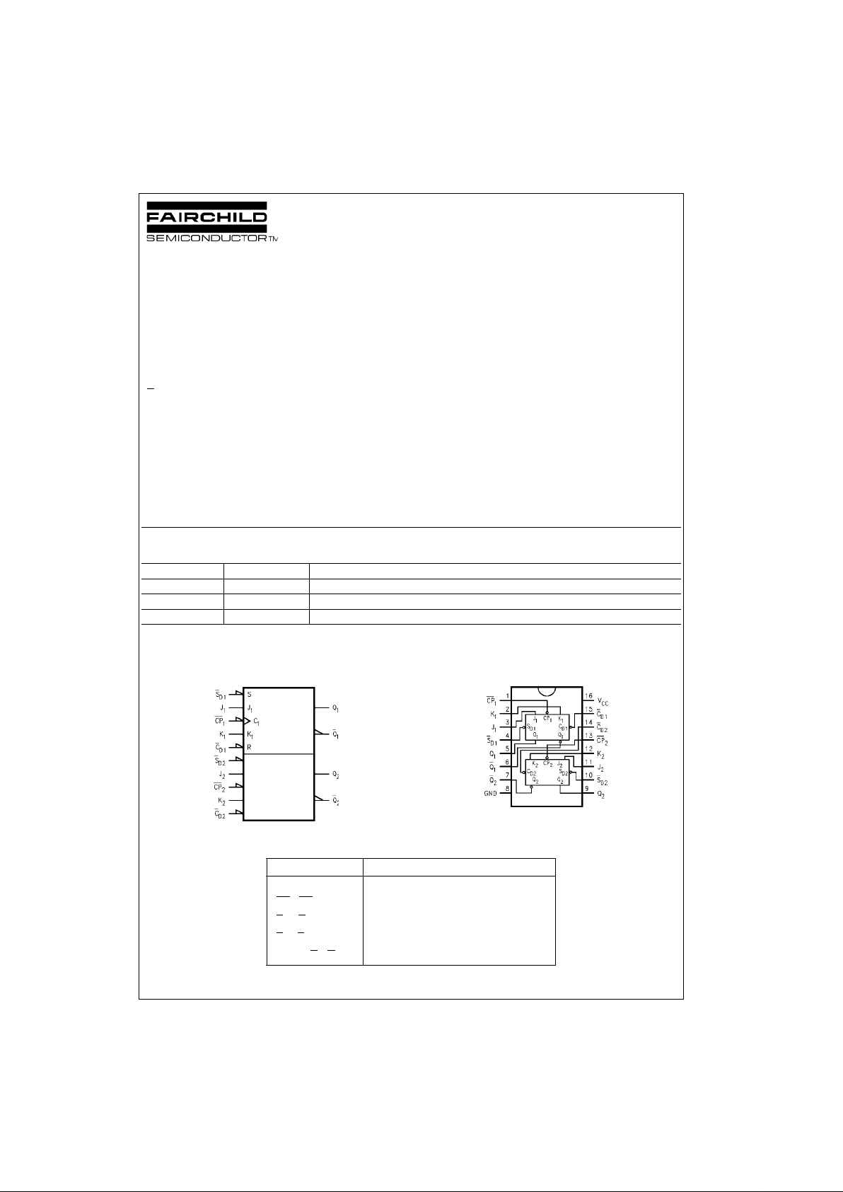
Logic Symbol
IEEE/IEC
Connection Diagram
Pin Descriptions
Order Number Package Number Package Description
74LCX112M M16A 16-Lead Small Outline Integrated Circuit (SOIC), JEDEC MS-012, 0.150” Narrow
74LCX112SJ M16D 16-Lead Small Outline Package (SOP), EIAJ TYPE II, 5.3mm Wide
74LCX112MTC MTC16 16-Lead Thin Shrink Small Outline Package (TSSOP), JEDEC MO-153, 4.4mm Wide
Pin Names Description
J
1
, J2, K1, K
2
Data Inputs
CP
1
, CP
2
Clock Pulse Inputs (Active Falling Edge)
C
D1
, C
D2
Direct Clear Inputs (Active LOW)
S
D1
, S
D2
Direct Set Inputs (Active LOW)
Q
1
, Q2, Q1, Q
2
Outputs
Page 2
www.fairchildsemi.com 2
74LCX112
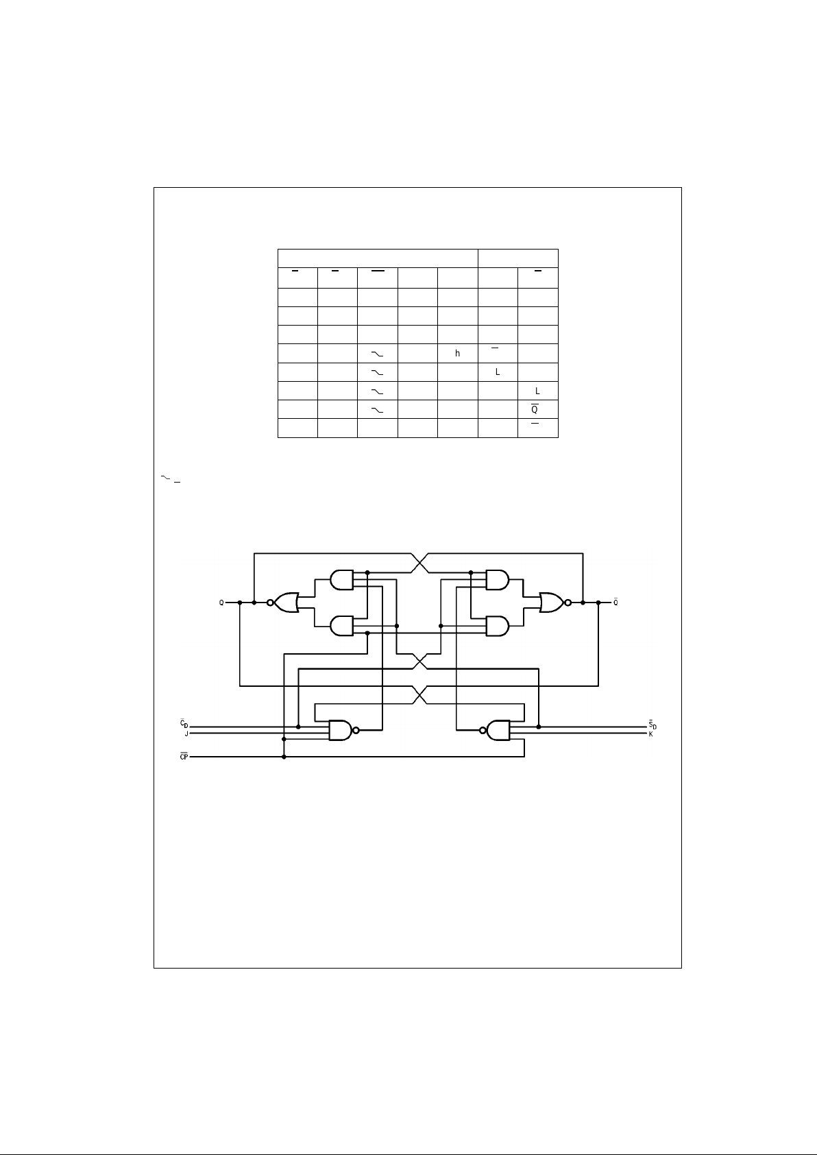
Truth Table
(Each half)
H(h) = HIGH Voltage Level
L(l) = LOW Voltage Level
X = Immaterial
= HIGH-to-LOW C loc k Transit ion
Q
O(QO
) = Before HIGH-to-LOW Transition of Clock
Lower case letters indicate the state of the ref erenced input or outp ut one setup time prior to the H I GH-to-LOW clock tra ns it ion.
Logic Diagram
Inputs Outputs
S
D
C
D
CP JKQQ
LHXXXHL
HLXXXLH
LLXXXHH
HH
hhQOQ
O
HH
lhLH
HH
hlHL
HH
llQOQ
O
HHHXXQOQ
O
Page 3
3 www.fairchildsemi.com
74LCX112
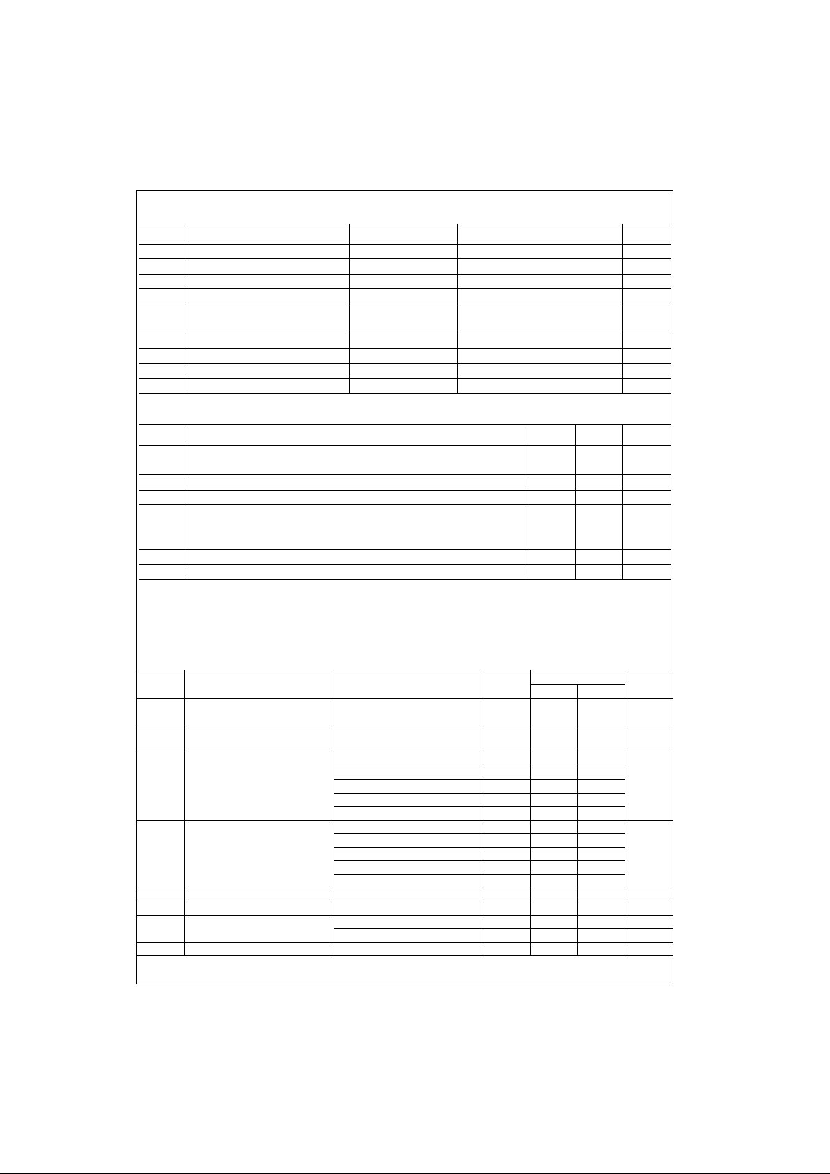
Absolute Maximum Ratings(Note 1)
Recommended Operating Conditions (Note 3)
Note 1: The Absolute Maximum Ratings are those values beyond which the safety of the device cannot be guaranteed. The device should not be operated
at these limits. The parametric values defined in the Electrical Characteristics tables are not guaranteed at the Absolute Maximum Ratings. The “Recommended Operating C onditions” table will def ine the conditions for act ual device operation.
Note 2: I
O
Absolute Maximum rating must be observed.
Note 3: Unused Inputs must be held HIGH or LOW. They may not float.
DC Electrical Characteristics
Symbol Parameter Value Conditions Units
V
CC
Supply Voltage −0.5 to +7.0 V
V
I
DC Input Voltage −0.5 to +7.0 V
V
O
DC Output Voltage −0.5 to V
CC
+ 0.5 Output in H IG H or L OW St at e ( Not e 2 ) V
I
IK
DC Input Diode Current −50 VI < GND mA
I
OK
DC Output Diode Current −50 VO < GND
mA
+50 V
O
> V
CC
I
O
DC Output Source/Sink Current ±50 mA
I
CC
DC Supple Current per Supply Pin ±100 mA
I
GND
DC Ground Current per Ground Pin ±100 mA
T
STG
Storage Temperature −65 to 150 °C
Symbol Parameter Min Max Units
V
CC
Supply Voltage Operating 2.0 3.6
V
Data Retention 1.5 3.6
V
I
Input Voltage 05.5V
V
O
Output Voltage HIGH or LOW State 0 V
CC
V
I
OH/IOL
Output Current VCC = 3.0V − 3.6V ±24
mAV
CC
= 2.7V − 3.0V ±12
V
CC
= 2.3V − 2.7V ±8
T
A
Free-Air Operating Temperature −40 85 °C
∆t/∆V Input Edge Rate, V
IN
= 0.8V−2.0V, VCC = 3.0V 0 10 ns/V
Symbol Parameter Conditions
V
CC
TA = 40°C to +85°C
Units
(V) Min Max
V
IH
HIGH Level Input Voltage 2.3 − 2.7 1.7 V
2.7 − 3.6 2.0
V
IL
LOW Level Input Voltage 2.3 − 2.7 0.7 V
2.7 − 3.6 0.8
V
OH
HIGH Level Output Voltage IOH = −100µA2.3 − 3.6 VCC - 0.2 0.7
IOH = -8 mA 2.3 1.8
V
IOH = −12 mA 2.7 2.2
IOH = −18 mA 3.0 2.4
IOH = −24 mA 3.0 2.2
V
OL
LOW Level Output Voltage IOL = 100µA2.3 − 3.6 0.6
IOL = 8mA 2.3 0.2
IOL = 12 mA 2.7 0.4 V
IOL = 16 mA 3.0 0.4
IOL = 24 mA 3.0 0.55
I
I
Input Leakage Current 0 ≤ II ≤ 5.5V 2.3 − 3.6 ±5.0 µA
I
OFF
Power-Off Leakage Current VI or VO = 5.5V 0 10 µA
I
CC
Quiescent Supply Current VI = VCC or GND 2.3 − 3.6 10 µA
3.6V ≤ VI ≤ 5.5V 2.3 − 3.6 ±10 µA
∆I
CC
Increase in ICC per Input VIH = VCC −0.6V 2.3 − 3.6 500 µA
Page 4
www.fairchildsemi.com 4
74LCX112
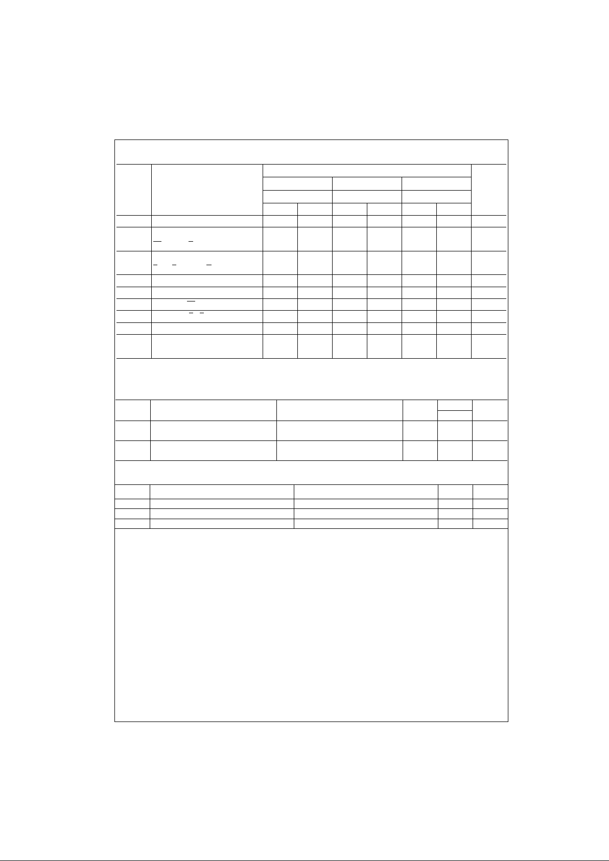
AC Electrical Characteristics
Note 4: Skew is defined as t he absolute value of t he difference betwee n t he actual propag at ion delay for any tw o separate outpu ts of the same device. T he
specification applies to any outputs swit c hing in the same directi on, eit her HIGH-to-LOW (t
OSHL
), or LOW-to-HIGH (t
OSLH
).
Dynamic Switching Characteristics
Capacitance
Symbol Parameters
TA = 40°C to 85°C, RL = 500Ω
Units
VCC = 3.3V ± 0.3V VCC = 2.7V V
CC =
2.5V ± 0.2V
CL=50 pF CL = 50 pF CL=30 pF
Min Max Min Max Min Max
f
MAX
Maximum Clock Frequency 150 150 150 MHz
t
PHL
Propagation Delay 1.5 7.5 1.5 8.0 1.5 9.0
ns
t
PLH
CPn to Qn or Q
n
1.57.51.58.01.59.0
t
PHL
Propagation Delay 1.5 7.0 1.5 8.0 1.5 8.4
ns
t
PLH
CDn or SDn to Qn or Q
n
1.57.01.78.01.58.4
t
S
Setup Time 2.5 2.5 4.0 ns
t
H
Hold Time 1.5 1.5 2.0 ns
t
W
Pulse Width CP 3.3 3.3 4.0 ns
t
W
Pulse Width (CD, SD) 3.3 3.3 4.0 ns
t
REC
Recovery Time 2.0 2.5 4.5 ns
t
OSHL
Output to Output Skew 1.0
ns
t
OSLH
(Note 4) 1.0
Symbol Parameter Conditions
V
CCTA
= 25°C
Units
(V) Typical
V
OLP
Quiet Output Dynamic Peak V
OL
CL = 50 pF, VIH = 3.3V, VIL = 0V 3.3 0.8
V
CL = 30 pF, VIH = 2.5V, VIL = 0V 2.5 0.6
V
OLV
Quiet Output Dynamic Valley V
OL
CL = 50 pF, VIH = 3.3V, VIL = 0V 3.3 −0.8
V
CL = 30 pF, VIH = 2.5V, VIL = 0V 2.5 −0.6
Symbol Parameter Conditions Typical Units
C
IN
Input Capacitance VCC = Open, VI = 0V or V
CC
7pF
C
OUT
Output Capacitance VCC = 3.3V, VI = 0V or V
CC
8pF
C
PD
Power Dissipation Capacitance VCC = 3.3V, VI = 0V or VCC, f = 10 MHz 25 pF
Page 5
5 www.fairchildsemi.com
74LCX112
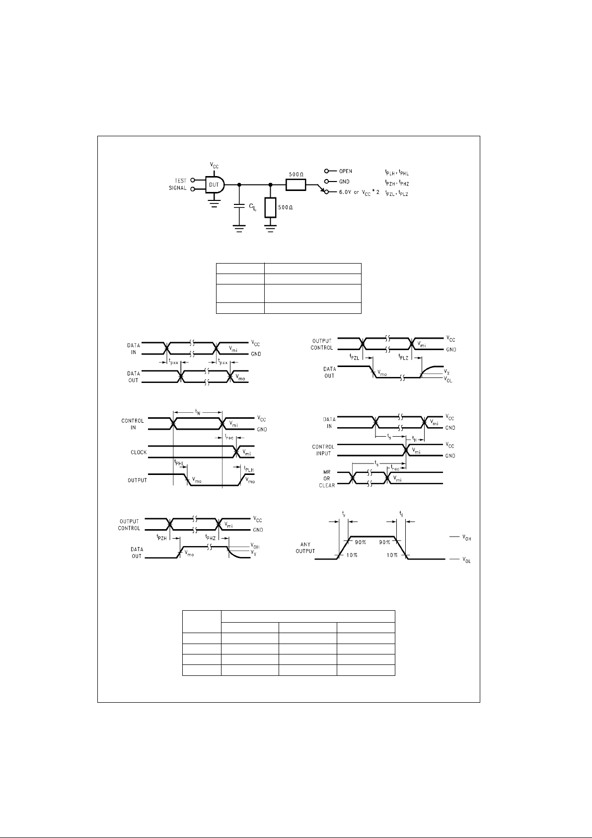
AC Loading and Waveforms Generic for LCX Family
FIGURE 1. AC Test Circuit
(C
L
includes probe and jig capacitance)
Waveform for Inverting and Non-Inverting Functions
Propagation Delay, Pulse Width and t
rec
Waveforms
3-STATE Output High Enable and
Disable TImes for Logic
3-STATE Output Low Enable and
Disable Times for Logic
Setup Time, Hold TIme and Recovery TIme for Logic
t
rise
and t
fall
FIGURE 2. Waveforms
(Input Pulse Characteristics; f=1MHz, t
r=tf
=3ns)
Test Switch
t
PLH
, t
PHL
Open
t
PZL
, t
PLZ
6V at VCC = 3.3 ± 0.3V
V
CC
x 2 at VCC = 2.5 ± 0.2V
t
PZH,tPHZ
GND
Symbol
V
CC
3.3V ± 0.3V 2.7V 2.5V ± 0.2V
V
mi
1.5V 1.5V VCC/2
V
mo
1.5V 1.5V VCC/2
V
x
VOL + 0.3V VOL + 0.3V VOL + 0.15V
V
y
VOH − 0.3V VOH − 0.3V VOH − 0.15V
Page 6
www.fairchildsemi.com 6
74LCX112
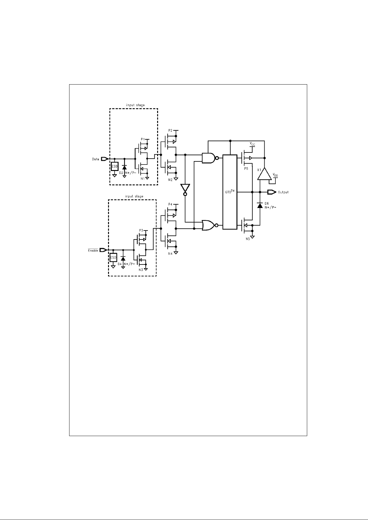
Schematic Diagram Generic for LCX Family
Page 7
7 www.fairchildsemi.com
74LCX112
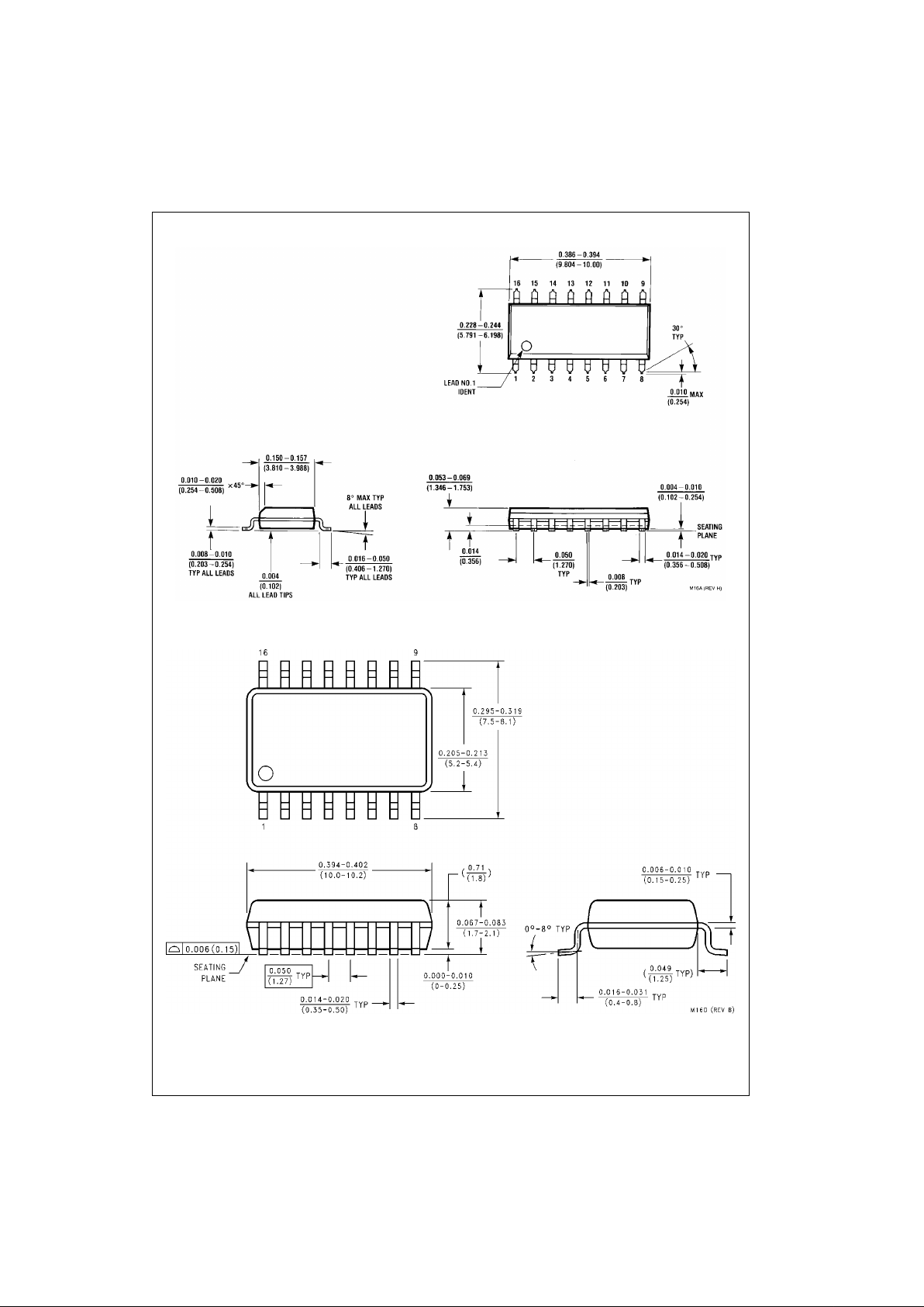
Physical Dimensions inches (millimeters) unless otherwise noted
16-Lead Small Outline Integrated Circuit (SOIC), JEDEC MS-012, 0.150” Narrow
Package Number M16A
16-Lead Small Outline Package (SOP), EIAJ TYPE II, 5.3mm Wide
Package Number M16D
Page 8
Fairchild does not assume any responsibility for use of any circuitry described, no circuit patent licenses are implied and Fairchild reserves the right at any time without notice to change said circuitry and specifications.
74LCX112 Low Voltage Dual J-K Negative Edge-Triggered Flip-Flop with 5V Tolerant Inputs
LIFE SUPPORT POLICY
FAIRCHILD’S PRODUCTS ARE NOT AUTHORIZED FOR USE AS CRITICAL COMPONENTS IN LIFE SUPPORT
DEVICES OR SYSTEMS WITHOUT THE EXPRESS WRITTEN APPROVAL OF THE PRESIDENT OF FAIRCHILD
SEMICONDUCTOR CORPORATION. As used herein:
1. Life support devices or systems are devices or syste ms
which, (a) are intended for surgical implant into the
body, or (b) support or sustain life, and (c) whose failure
to perform when properly used in accordance with
instructions for use provided in the labeling, can be reasonably expected to result in a significant inju ry to the
user.
2. A critical component i n any compon ent of a lif e support
device or system whose failu re to perform can be reasonably expected to ca use the fa i lure of the life su pp ort
device or system, or to affect its safety or effectiveness.
www.fairchildsemi.com
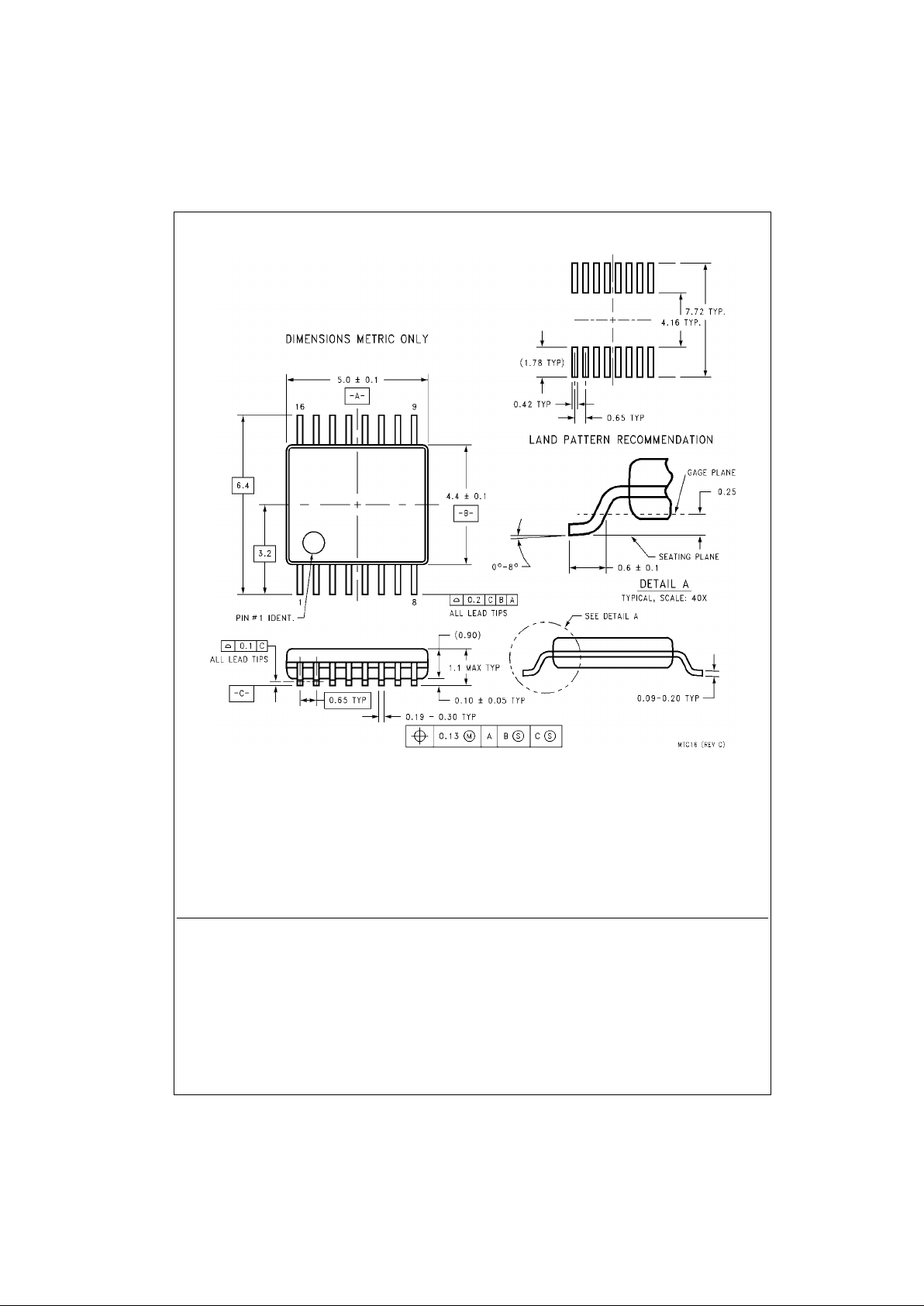
Physical Dimensions inches (millimeters) unless otherwise noted (Continued)
16-Lead Thin Shrink Small Outline Package (TSSOP), JEDEC MO-153, 4.4mm Wide
Package Number MTC16
 Loading...