

Datasheet 74LCX07SJX, 74LCX07SJ, 74LCX07MX, 74LCX07MTCX, 74LCX07MTC Datasheet (Fairchild Semiconductor)
...Page 1
© 1999 Fairchild Semiconductor Corporation DS500238 www.fairchildsemi.com
October 1999
Revised November 1999
74LCX07 Low Voltage Hex Buffer with Open Drain Outputs
74LCX07
Low Voltage Hex Buffer with Open Drain Outputs
General Description
The LCX07 contains six buffers. The inputs t olerate voltages up to 7V allowing the interface of 5V syste ms to 3V
systems.
The outputs of the LCX07 ar e open drain and can be connected to other open drain outputs to implement active
HIGH wire AND or active LOW wire OR functions.
The 74LCX07 is fabricat ed with advanced CMO S technology to achieve high speed operation while maintaining
CMOS low power dissipation.
Features
■ 5V tolerant inputs
■ 2.3V–5.5V V
CC
specifications provided
■ 2.9 ns t
PD
max (V
CC
= 3.3V), 10 µA ICC max
■ Power down high impedance inputs and outputs
■ ±24 mA output drive (V
CC
= 3.0V)
■ Implements patented noise/EMI reduction circuitry
■ Latch-up performance exce eds 500 mA
■ ESD performance:
Human body model > 2000V
Machine model > 200V
Ordering Code:
Devices also availab le in Tape and Reel. Specify by appending th e s uffix let t er “X” to the ordering code.
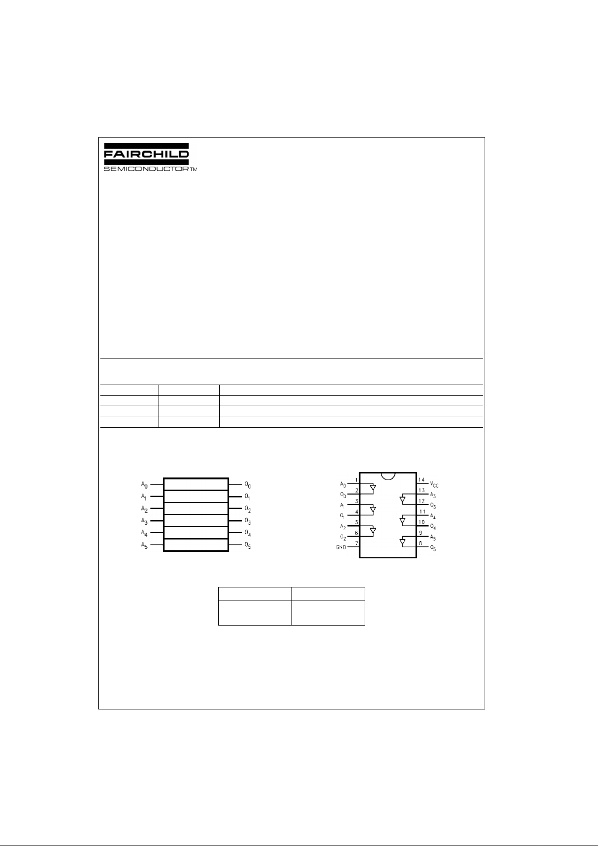
Logic Symbol
IEEE/IEC
Connection Diagram
Pin Descriptions
Order Number Package Number Package Description
74LCX07M M14A 14-Lead Small Outline Integrated Circuit (SOIC), JEDEC MS-120, 0.150” Narrow
74LCX07SJ M14D 14-Lead Small Outline Package (SOP), EIAJ TYPE II, 5.3mm Wide
74LCX07MTC MTC14 14-Lead Thin Shrink Small Outline Package (TSSOP), JEDEC MO-153, 4.4mm Wide
Pin Names Description
A
n
Inputs
O
n
Outputs
Page 2
www.fairchildsemi.com 2
74LCX07
Absolute Maximum Ratings(Note 1)
Recommended Operating Conditions (Note 3)
Note 1: The Absolute Maximum Ratings are those values beyond which the safety of the device cannot be guaranteed. The device should not be operated
at these limits. The pa rametric values defined in the Elec trical Characte ristics tables are n ot guaranteed at the Absolute Ma ximum Ratings. The Recommended Operating Conditions table will define the conditions for actual device operation.
Note 2: I
O
Absolute Maximum Rating must be observed.
Note 3: Unused inputs must be held HIGH or LOW. They may not float.
DC Electrical Characteristics
Symbol Parameter Value Conditions Units
V
CC
Supply Voltage −0.5 to +7.0 V
V
I
DC Input Voltage −0.5 to +7.0 V
V
O
DC Output Voltage −0.5 to VCC + 0.5 Output in HIGH or LOW State (Note 2) V
I
IK
DC Input Diode Current −50 VI < GND mA
I
OK
DC Output Diode Current −50 VO < GND
mA
+50 V
O
> V
CC
I
O
DC Output Source/Sink Current ±50 mA
I
CC
DC Supply Current per Supply Pin ±100 mA
I
GND
DC Ground Current per Ground Pin ±100 mA
T
STG
Storage Temperature −65 to +150 °C
Symbol Parameter Min Max Units
V
CC
Supply Voltage Operating 2.0 5.5
V
Data Retention 1.5 5.5
V
I
Input Voltage 05.5V
V
O
Output Voltage HIGH or LOW State 0 V
CC
V
I
OL
Output Current VCC = 4.5 − 5.5V +32
mA
V
CC
= 3.0V − 3.6V +24
V
CC
= 2.7V − 3.0V +12
V
CC
= 2.3V − 2.7V +8
T
A
Free-Air Operating Temp erature −40 85 °C
∆t/∆V Input Edge Rate, V
IN
= 0.8V–2.0V, VCC = 3.0V 0 10 ns/V
Symbol Parameter Conditions
V
CCTA
= −40°C to +85°C
Units
(V) Min Max
V
IH
HIGH Level Input Voltage 2.3 − 2.7 1.7
V2.7 − 3.6 2.0
4.5 − 5.5 0.7 x V
CC
V
IL
LOW Level Input Voltage 2.3 − 2.7 0.7
V2.7 − 3.6 0.8
4.5 - 5.5 0.3 x V
CC
V
OL
LOW Level Output Voltage IOL = −100 µA2.3 − 5.5 0.2
V
IOL = 8 mA 2.3 0.6
IOL = 12 mA 2.7 0.4
IOL = 16 mA 3.0 0.4
IOL = 24 mA 3.0 0.55
IOL = 32 mA 4.5 0.55
I
I
Input Leakage Current 0 ≤ VI ≤ 5.5V 2.3 − 5.5 ±5.0 µA
I
OFF
Power-Off Leakage Current VI or VO = 5.5V 0 10 µA
I
CC
Quiescent Supply Current VI = VCC or GND 2.3 − 5.5 10
µA
3.6V ≤ VI ≤ 5.5V 2.3 − 5.5 ±10
∆I
CC
Increase in ICC per Input VIH = VCC −0.6V 2.3 − 3.6 500 µA
4.5 − 5.5 1 mA
Page 3

3 www.fairchildsemi.com
74LCX07
AC Electrical Characteristics
Note 4: Skew is defined as t he absolute value of t he difference between the actual propagation delay for any two separate outputs of the same device. The
specification applies t o any outputs switching in th e s am e direction, either HIG H -t o-LOW (t
OSHL
) or LOW-to-HIGH (t
OSLH
).
Dynamic Switching Characteristics
Capacitance
Symbol Parameter
T
A
= −40°C to +85°C, RL = 500Ω
Units
V
CC
= 5.0V ± 0.5V VCC = 3.3V ± 0.3V VCC = 2.7V VCC = 2.5V ± 0.2V
C
L
= 50 pF CL= 50 pF CL= 50 pF CL= 30 pF
Min Max Min Max Min Max Min Max
t
PZL
Propagation Delay Time 0.5 3.0 0.8 3.7 1.0 4.4 0.8 3.8
ns
t
PLZ
0.5 3.0 0.8 3.7 1.0 4.4 0.8 3.8
Symbol Parameter Conditions
V
CCTA
= 25°C
Units
(V) Typical
V
OLP
Quiet Output Dynamic Peak V
OL
CL = 50 pF, VIH = 3.3V, VIL = 0V 3. 3 0.9
V
CL = 30 pF, VIH = 2.5V, VIL = 0V 2. 5 0.7
V
OLV
Quiet Output Dynamic Valley V
OL
CL = 50 pF, VIH = 3.3V, VIL = 0V 3.3 −0.8
V
CL = 30 pF, VIH = 2.5V, VIL = 0V 2.5 −0.6
Symbol Parameter Conditions Typical Units
C
IN
Input Capacitance VCC = Open, VI = 0V or V
CC
7pF
C
OUT
Output Capacitance VCC = 3.3V, VI = 0V or V
CC
8pF
C
PD
Power Dissipation Capacitance VCC = 3.3V, VI = 0V or VCC, f = 10 MHz 25 pF
Page 4

www.fairchildsemi.com 4
74LCX07
AC Loading and Waveforms
FIGURE 1. AC Test Circuit
(C
L
includes probe and jig capacitance)
3-STATE Output Low Enable and
Disable Times for Logic
t
rise
and t
fall
FIGURE 2. Waveforms
(Input Pulse Characteristi cs; f =1MHz, t
r
= tf = 3ns)
Test Switch
t
PZL
, t
PLZ
VCC x 2 at VCC = 5.0 ± 0.5V
6V at V
CC
= 3.3 ± 0.3V
V
CC
x 2 at VCC = 2.5 ± 0.2V
Symbol
V
CC
5.0V ± 0.5V 3.3V ± 0.3V 2.7V 2.5V ± 0.2V
V
mi
VCC/2 1.5V 1.5V VCC/2
V
mo
VCC/2 1.5V 1.5V VCC/2
V
x
VOL + 0.3V VOL + 0.3V VOL + 0.3V VOL + 0.15V
V
y
VOH − 0.3V VOH − 0.3V VOH − 0.3V VOH − 0.15V
Page 5

5 www.fairchildsemi.com
74LCX07
Physical Dimensions inches (millimeters) unless otherwise noted
14-Lead Small Outline Integrated Circuit (SOIC), JEDEC MS-120, 0.150” Narrow
Package Number M14A
14-Lead Small Outline Package (SOP), EIAJ TYPE II, 5.3mm Wide
Package Number M14D
Page 6

www.fairchildsemi.com 6
74LCX07 Low Voltage Hex Buffer with Open Drain Outputs
Physical Dimensions inches (millimeters) unless otherwise noted (Continued)
14-Lead Thin Shrink Small Outline Package (TSSOP), JEDEC MO-153, 4.4mm Wide
Package Number MTC14
Fairchild does not assume any responsibility for use of any circuitr y described, no circuit patent licenses are implied and
Fairchild reserves the right at any time without notice to change said circuitry and specifications.
LIFE SUPPORT POLICY
FAIRCHILD’S PRODUCTS ARE NOT AUTHORIZED FOR USE AS CRITICAL COMPONENTS IN LIFE SUPPORT
DEVICES OR SYSTEMS WITHOUT THE EXPRESS WRITTEN APPROVAL OF THE PRESIDENT OF FAIRCHILD
SEMICONDUCTOR CORPORATION. As used herein:
1. Life support devices or systems are devices or syste ms
which, (a) are intended for surgical implant into the
body, or (b) support or sustain life, and (c) whose failure
to perform when properly used in accordance with
instructions for use provided in the labeling, can be reasonably expected to result in a significant inju ry to the
user.
2. A critical component in any compon ent of a lif e supp ort
device or system whose failure t o perform can be reasonably expected to ca use the failure of the life supp ort
device or system, or to affect its safety or effectiveness.
www.fairchildsemi.com
 Loading...