

Page 1
1/10May 2003
■ 5V TOLERANT INPUTS
■ HIGH SPEED :
t
PD
= 5.2ns (MAX.) at VCC=3V
■ POWER DOWN PROTECTION ON INPUTS
AND OUTPUTS
■ SYMMETRICAL OUTPUT IMPEDANCE:
|I
OH
|=IOL= 24mA (MIN) at VCC=3V
■ PCI BUS LEVELS GUARANTEED AT 24 mA
■ OPERATING VOLTAGE RANGE:
V
CC
(OPR) = 2.0V to 3.6V (1.5V Data
Retention)
■ PIN AND FUNCTION COMPATIBLE WITH
74 SERIES 07
■ LATCH-UP PERFORMANCE EXCEEDS
500mA (JESD 17)
■ ESD PERFORMANCE:
HBM > 2 000V (MIL STD 883 method 3015);
MM > 200V
DESCRIPTION
The 74LCX07 is a low voltage CMOS OPEN
DRAIN HEX BUFFER fabricated with sub-micron
silicon gate and double-layer me tal wiring C
2
MOS
technology. It is ideal for low power and high
speed 3.3V applications. It canbeinterfaced to 5V
signal environment for inputs.
The internal circuit is composed of 2 stages
including buffer output, which provides high noise
immunity and stable output.
It has same speed performance at 3.3V than 5V
AC/ACT family, combined with a lower power
consumption.
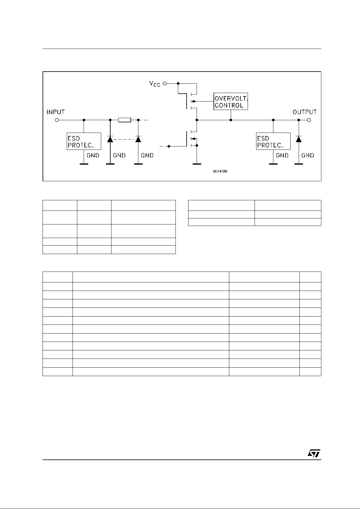
All inputs and outputs are equipped with
protection circuits against stat ic discharge, giving
them 2K V ESD imm unit y and transient excess
voltage.
74LCX07
LOW VOLTAGE CMOS HEX BUFFER (OPEN DRAIN)
WITH 5V TOLERANT INPUTS
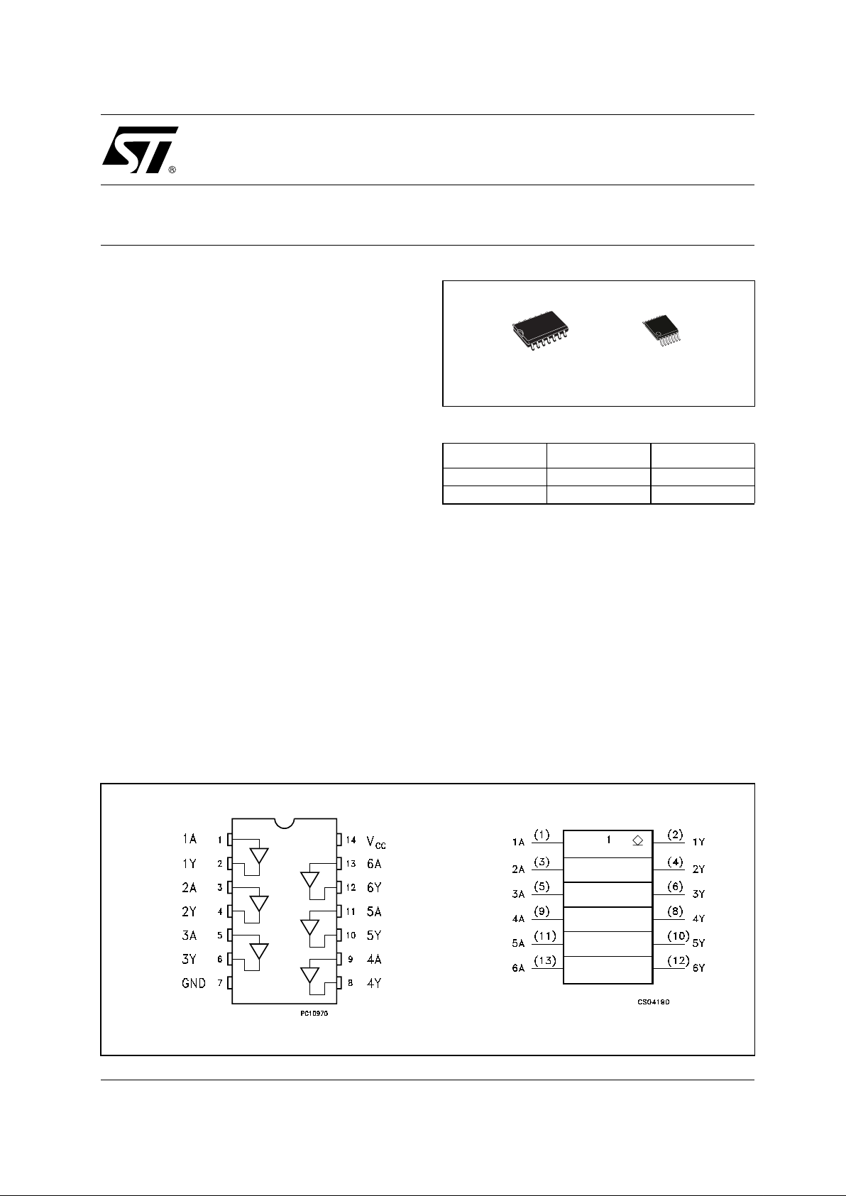
PIN CONNECTION AND IEC LOGIC SYMBOLS
ORDER CODES
PACKAGE TUBE T & R
SOP 74LCX07M 74LCX07MTR
TSSOP 74LCX07TTR
TSSOPSOP
Page 2
74LCX07
2/10
INPUT AND OUTPUT EQUIVALENT CIRCUIT
PIN DESCRIPTION TRUTH TABLE
Z : High Impedance
ABSOLUTE MAXIMUM RATINGS
Absolute Maximum Ratings are those values beyond which damage to the device may occur. Functional operation under these conditions is
not implied
1) I
O
absolute maximum rating must be observed
2) VO<GND
PIN No SYMBOL NAME AND FUNCTION
1, 3, 5, 9, 11,
13
1A to 6A Data Inputs
2, 4, 6, 8, 10,
12
1Y to 6Y Data Outputs
7 GND Ground (0V)
14
V
CC
Positive Supply Voltage
AY
LL
HZ
Symbol Parameter Value Unit
V
CC
Supply Voltage
-0.5 to +7.0 V
V
I
DC Input Voltage
-0.5 to +7.0 V
V
O
DC Output Voltage (VCC= 0V)
-0.5 to +7.0 V
V
O
DC Output Voltage (High or Low State) (note 1) -0.5 to VCC+ 0.5
V
I
IK
DC Input Diode Current
-50 mA
I
OK
DC Output Diode Current (note 2)
-50 mA
I
O
DC Output Current
± 50 mA
I
CC
DC Supply Current per Supply Pin
± 100 mA
I
GND
DC Ground Current per Supply Pin
± 100 mA
T
stg
Storage Temperature
-65 to +150 °C
T
L
Lead Temperature (10 sec)
300 °C
Page 3
74LCX07
3/10
RECOMMENDED OPERATING CONDITIONS
1) Truth Table guaranteed: 1.5V to 3.6V
2) V
IN
from0.8V to 2V at VCC=3.0V
DC SPECIFICATIONS
DYNAMIC SWITCHING CHARACTERISTICS
1) Numberof outputsdefined as"n". Measured with"n-1" outputs switching fromHIGH to LOW orLOWto HIGH. The remaining outputis
measured in the LOW state.
Symbol Parameter Value Unit
V
CC
Supply Voltage (note 1)
2.0 to 3.6 V
V
I
Input Voltage
0 to 5.5 V
V
O
Output Voltage (VCC= 0V)
0 to 5.5 V
V
O
Output Voltage (High or Low State) 0 to V
CC
V
I
OH,IOL
High or Low Level Output Current (VCC= 3.0 to 3.6V)
± 24 mA
I
OH,IOL
High or Low Level Output Current (VCC= 2.7V)
± 12 mA
T
op
Operating Temperature
-55 to 125 °C
dt/dv Input Rise and Fall Time (note 2) 0 to 10 ns/V
Symbol Parameter
Test Condition Value
Unit
V
CC
(V)
-40to85°C -55to125°C
Min. Max. Min. Max.
V
IH
High Level Input
Voltage
2.7to3.6
2.0 2.0 V
V
IL
Low Level Input
Voltage
0.8 0.8 V
V
OL
Low Level Output
Voltage
2.7to3.6
IO=100 µA
0.2 0.2
V
2.7
I
O
=12 mA
0.4 0.4
3.0
I
O
=16 mA
0.4 0.4
I
O
=24 mA
0.55 0.55
I
I
Input Leakage
Current
2.7to3.6
V
I
= 0 to 5.5V
± 5 ± 5 µA
I
off
Power Off Leakage
Current
0
V
I
or VO=5.5V
10 10 µA
I
OZ
High Impedance
Output Leakage
Current
2.7to3.6
V
I=VIH
or V
IL
VO= 0 to V
CC
± 5 ± 5 µA
I
CC
Quiescent Supply
Current
2.7to3.6
VI=VCCor GND
10 10
µA
V
I
or VO= 3.6 to 5.5V
± 10 ± 10
∆I
CC
ICCincr. per Input
2.7to3.6
VIH=VCC-0.6V
500 500 µA
Symbol Parameter
Test Condition Value
Unit
V
CC
(V)
T
A
=25°C
Min. Typ. Max.
V
OLP
Dynamic Low Level Quiet
Output (note 1)
3.3
V
IL
=0V
V
IH
= 3.3V
0.8
V
V
OLV
-0.8
Page 4

74LCX07
4/10
AC ELECTRICAL CHARACTERISTICS
1) Skew is defined as the absolute value of the difference between the actual propagation delay for any two outputs of the same device switching in the same direction, either HIGH or LOW (t
OSLH
=|t
PLHm-tPLHn
|, t
OSHL
=|t
PHLm-tPHLn
|)
2) Parameter guaranteed by design
CAPACITIVE CHARACTERISTICS
1) CPDis defined as the value of the IC’s internal equivalent capacitance which is calculated from the operating current consumption without
load. (Refer to Test Circuit). Average operating current can be obtained by the following equation. I
CC(opr)=CPDxVCCxfIN+ICC
/6 (per gate)
TEST CIRCUIT
CL= 50 pF or equivalent (includes jig and probe capacitance)
R
L
=R1=500Ω or equivalent
R
T=ZOUT
of pulse generator (typically 50Ω)
Symbol Parameter
Test Condition Value
Unit
V
CC
(V)
C
L
(pF)
R
L
(Ω)
t
s
= t
r
(ns)
-40 to 85 °C -55 to 125 °C
Min. Max. Min. Max.
t
PLZ
Propagation Delay
Time
2.7
50 500 2.5
7.0 7.0
ns
3.0 to 3.6 1.0 5.2 1.0 5.2
t
PZL
Propagation Delay
Time
2.7
50 500 2.5
7.0 7.0
ns
3.0 to 3.6 1.0 5.2 1.0 5.2
t
OSLH
t
OSHL
Output To Output
Skew Time (note1,
2)
3.0 to 3.6 50 500 2.5 1.0 1.0 ns
Symbol Parameter
Test Condition Value
Unit
V
CC
(V)
T
A
=25°C
Min. Typ. Max.
C
IN
Input Capacitance
3.3
VIN= 0 to V
CC
6pF
C
OUT
Output Capacitance
3.3
VIN= 0 to V
CC
14 pF
C
PD
Power Dissipation Capacitance
(note 1)
3.3 fIN= 10MHz
V
IN
= 0 or V
CC
4.3
pF
TEST SWITCH
t
PLH,tPHL
Open
t
PZL,tPLZ
6V
t
PZH,tPHZ
GND
Page 5

74LCX07
5/10
WAVEFORM : PROPAGATION DELAY (f=1MHz; 50% duty cycle)
Page 6

74LCX07
6/10
DIM.
mm. inch
MIN. TYP MAX. MIN. TYP. MAX.
A 1.75 0.068
a1 0.1 0.2 0.003 0.007
a2 1.65 0.064
b 0.35 0.46 0.013 0.018
b1 0.19 0.25 0.007 0.010
C 0.5 0.019
c1 45˚ (typ.)
D 8.55 8.75 0.336 0.344
E 5.8 6. 2 0.228 0.244
e 1.27 0.050
e3 7.62 0.300
F 3.8 4.0 0.149 0.157
G 4.6 5.3 0.181 0.208
L 0.5 1.27 0.019 0.050
M 0.68 0.026
S ˚ (max.)
SO-14 MECHANICAL DATA
PO13G
8
Page 7

74LCX07
7/10
DIM.
mm. inch
MIN. TYP MAX. MIN. TYP. MAX.
A 1.2 0.047
A1 0.05 0.15 0.002 0.004 0.006
A2 0.8 1 1.05 0.031 0.039 0.041
b 0.19 0.30 0.007 0.012
c 0.09 0.20 0.004 0.0089
D 4.9 5 5.1 0.193 0.197 0.201
E 6.2 6.4 6.6 0.244 0.252 0.260
E1 4.3 4.4 4.48 0.169 0.173 0.176
e 0.65 BSC 0.0256 BSC
K0˚ 8˚0˚ 8˚
L 0.45 0.60 0.75 0.018 0.024 0.030
TSSOP14 MECHANICAL DATA
c
E
b
A2
A
E1
D
1
PIN 1 IDENTIFICATION
A1
L
K
e
0080337D
Page 8

74LCX07
8/10
DIM.
mm. inch
MIN. TYP MAX. MIN. TYP. MAX.
A 330 12.992
C 12.8 13.2 0.504 0.519
D 20.2 0.795
N 60 2.362
T 22.4 0.882
Ao 6.4 6.6 0.252 0.260
Bo 9 9.2 0.354 0.362
Ko 2.1 2.3 0.082 0.090
Po 3.9 4.1 0.153 0.161
P 7.9 8.1 0.311 0.319
Tape & Reel SO-14 MECHANICAL DATA
Page 9

74LCX07
9/10
DIM.
mm. inch
MIN. TYP MAX. MIN. TYP. MAX.
A 330 12.992
C 12.8 13.2 0.504 0.519
D 20.2 0.795
N 60 2.362
T 22.4 0.882
Ao 6.7 6.9 0.264 0.272
Bo 5.3 5.5 0.209 0.217
Ko 1.6 1.8 0.063 0.071
Po 3.9 4.1 0.153 0.161
P 7.9 8.1 0.311 0.319
Tape & Reel TSSOP14 MECHANICAL DATA
Page 10

74LCX07
10/10
Information furnished is believed to be accurate and reliable. However, STMicroelectronics assumes no responsibility for the
consequences of use o f suc h inf ormat ion n or f or an y infr ingeme nt of paten ts or oth er ri gh ts of third part ies whic h may resul t f rom
its use. No license is granted by implication or otherwise under any patent or patent rights of STMicroelectronics. Specifications
mentioned in this publication are subject to change without notice. This publication supersedes and replaces all information
previously supplied. STMicroelectronics products are not authorized for use as critical components in life support devices or
systems without express written approval of STMicroelectronics.
© The ST logo is a registered trademark of STMicroelectronics
© 2003 STMicroelectronics - Printed in Italy - All Rights Reserved
STMicroelectronics GROUP OF COMPANIES
Australia - Brazil - Canada - China - Finland - France - Germany - Hong Kong - India - Israel - Italy - Japan - Malaysia - Malta - Morocco
Singapore - Spain - Sweden - Switzerland - United Kingdom - United States.
© http://www.st.com
 Loading...