

Page 1
1/8September 2001
■ 5V TOLERANT INPUTS
■ HIGH SPEED :
t
PD
= 5.2ns (MAX.) at VCC = 3V
■ POWER DOWN PROTECTION ON INPUT S
AND OUTPUTS
■ SYMMETRICAL OUTPUT IMPEDANCE:
|I
OH
| = IOL = 24mA (MIN) at VCC = 3V
■ PCI BUS LEVELS GUARANT EED AT 2 4 mA
■ OPERATING VOLTAGE RANGE:
V
CC
(OPR) = 2.0V to 3.6V (1.5V Data
Retention)
■ PIN AND FUNCTION COMPATIBLE WITH
74 SERIES 05
■ LATCH-UP PERFORMANCE EXCEEDS
500mA (JESD 17)
■ ESD PERFORMANCE:
HBM > 2000V (MIL STD 883 method 3015);
MM > 200V
DESCRIPTION
The 74LCX05 is a low voltage CMOS OPEN
DRAIN HEX INVERTER fabricated with
sub-micron silicon gate and double-layer metal
wiring C
2
MOS technology. It is ideal for low power
and high speed 3.3V applications. It can be
interfaced to 5V signal environment for inputs.
The internal circuit is composed of 3 stages
including buffer ou tput, which provides high noise
immunity and stable output.
It has same speed performance at 3. 3V than 5V
AC/ACT family, combined with a lower power
consumption.
All inputs and outputs are equipped with
protection circuits against stat ic discharge, giving
them 2KV ESD immunity and transient excess
voltage.
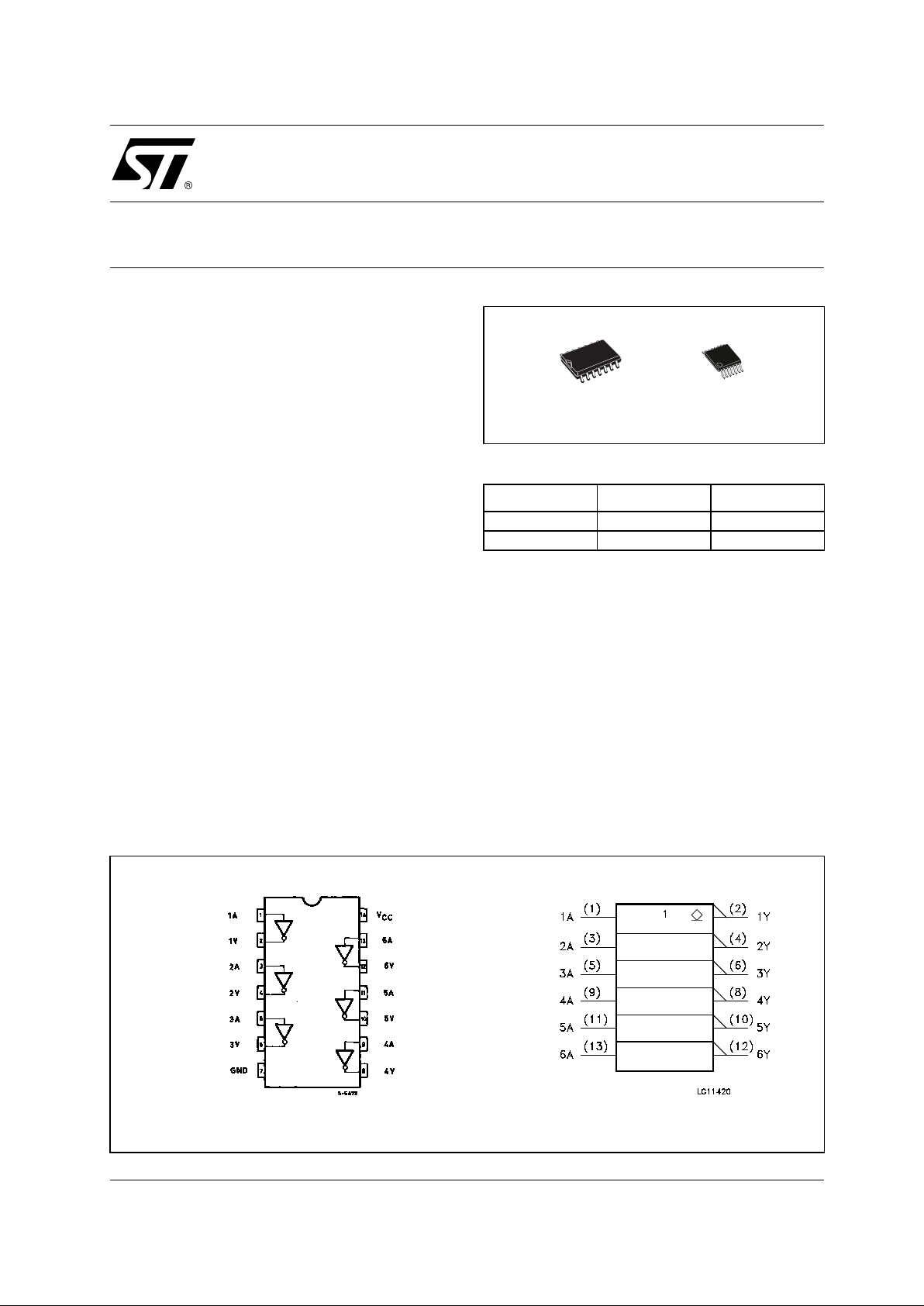
74LCX05
LOW VOLTAGE CMOS HEX INVERTER (OPEN DRAIN)
WITH 5V TOLERANT INPUTS
PIN CONNECTION AND IEC LOGIC SYMBOLS
ORDER CODES
PACKAGE TUBE T & R
SOP 74LCX05M 74LCX05MTR
TSSOP 74LCX05TTR
TSSOPSOP
Page 2
74LCX05
2/8
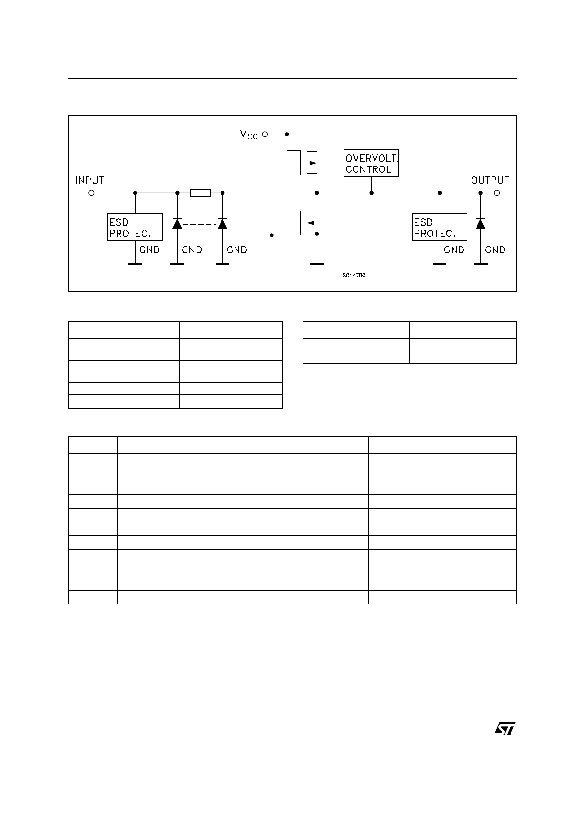
INPUT AND OUTPUT EQUIVALENT CIRCUIT
PIN DESCRIPTION TRUTH TABLE
Z : High Impedance
ABSOLUTE MAXIMUM RATINGS
Absolute Maximum Ratings are those values beyond which damage to the device may occur. Functional operation under these conditions is
not implied
1) I
O
absolute ma xim um rating must be observ ed
2) V
O
< GND
PIN No SYMBOL NAME AND FUNCTION
1, 3, 5, 9, 1 1,
13
1A to 6A Data Inputs
2, 4, 6, 8, 10,
12
1Y to 6Y Data Outputs
7 GND Ground (0V)
14
V
CC
Positive Supply Voltage
AY
LZ
HL
Symbol Parameter Value Unit
V
CC
Supply Voltage
-0.5 to +7.0 V
V
I
DC Input Voltage
-0.5 to +7.0 V
V
O
DC Output Voltage (VCC = 0V)
-0.5 to +7.0 V
V
O
DC Output Voltage (High or Low State) (note 1) -0.5 to VCC + 0.5
V
I
IK
DC Input Diode Current
- 50 mA
I
OK
DC Output Diode Current (note 2)
- 50 mA
I
O
DC Output Current
± 50 mA
I
CC
DC Supply Current per Supply Pin
± 100 mA
I
GND
DC Ground Current per Supply Pin
± 100 mA
T
stg
Storage Temperature
-65 to +150 °C
T
L
Lead Temperature (10 sec)
300 °C
Page 3
74LCX05
3/8
RECOMMENDED OPERATING CONDITIONS
1) Truth T abl e guarante ed: 1.5V to 3.6 V
2) V
IN
from 0.8V to 2V at VCC = 3.0V
DC SPECIFICATIONS
DYNAMIC SWITCHING CHARACTERISTICS
1) Number of outputs defined as "n". Meas ured with "n- 1" outputs swi t ching from HIGH to LOW or LOW to HIGH . The remaini ng output is
measur ed i n the LOW sta te.
Symbol Parameter Value Unit
V
CC
Supply Voltage (note 1)
2.0 to 3.6 V
V
I
Input Voltage
0 to 5.5 V
V
O
Output Voltage (VCC = 0V)
0 to 5.5 V
V
O
Output Voltage (High or Low State) 0 to V
CC
V
I
OH
, I
OL
High or Low Level Output Current (VCC = 3.0 to 3.6V)
± 24 mA
I
OH
, I
OL
High or Low Level Output Current (VCC = 2.7V)
± 12 mA
T
op
Operating Temperature
-55 to 125 °C
dt/dv Input Rise and Fall Time (note 2) 0 to 10 ns/V
Symbol Parameter
Test Condition Value
Unit
V
CC
(V)
-40 to 85 °C -55 to 125 °C
Min. Max. Min. Max.
V
IH
High Level Input
Voltage
2.7 to 3.6
2.0 2.0 V
V
IL
Low Level Input
Voltage
0.8 0.8 V
V
OL
Low Level Output
Voltage
2.7 to 3.6
I
O
=100 µA
0.2 0.2
V
2.7
I
O
=12 mA
0.4 0.4
3.0
I
O
=16 mA
0.4 0.4
I
O
=24 mA
0.55 0.55
I
I
Input Leakage
Current
2.7 to 3.6
V
I
= 0 to 5.5V
± 5 ± 5 µA
I
off
Power Off Leakage
Current
0
V
I
or VO = 5.5V
10 10 µA
I
OZ
High Impedance
Output Leakage
Current
2.7 to 3.6
V
I
= VIH or V
IL
VO = 0 to V
CC
± 5 ± 5 µA
I
CC
Quiescent Supply
Current
2.7 to 3.6
VI = VCC or GND
10 10
µA
V
I
or VO= 3.6 to 5.5V
± 10 ± 10
∆I
CC
ICC incr. per Input
2.7 to 3.6
VIH = VCC - 0.6V
500 500 µA
Symbol Parameter
Test Condition Value
Unit
V
CC
(V)
T
A
= 25 °C
Min. Typ. Max.
V
OLP
Dynamic Low Level Quiet
Output (note 1)
3.3
V
IL
= 0V
V
IH
= 3.3V
0.8
V
V
OLV
-0.8
Page 4
74LCX05
4/8
AC ELECTRICAL CHARACTERISTICS
1) Skew is defined as the absolute value of the difference between the actual propagation delay for any two outputs of the same device switching in the same direction, either HIGH or LOW ( t
OSLH
= | t
PLHm
- t
PLHn
|, t
OSHL
= | t
PHLm
- t
PHLn
|)
2) Param eter guaranteed by design
CAPACITIVE CHARACTERISTICS
1) CPD is defined as the value of the IC’s internal equivalent capacitance which is calculated from the operating current consumption without
load. (Refer to Test Circuit). Average operating current can be obtained by the following equation. I
CC(opr)
= CPD x VCC x fIN + ICC/6 (per gate)
TEST CIRCUIT
CL = 50 pF or equival ent (includes jig and pr obe capacitance)
R
L
= R1 = 500Ω or equivalent
R
T
= Z
OUT
of pulse generator (typically 50Ω)
Symbol Parameter
Test Condition Value
Unit
V
CC
(V)
C
L
(pF)
R
L
(Ω)
t
s
= t
r
(ns)
-40 to 85 °C -55 to 125 °C
Min. Max. Min. Max.
t
PLZ
Propagation Delay
Time
2.7
50 500 2 .5
6.5 6.5
ns
3.0 to 3.6 1.0 5.2 1.0 5.2
t
PZL
Propagation Delay
Time
2.7
50 500 2 .5
6.5 6.5
ns
3.0 to 3.6 1.0 5.2 1.0 5.2
t
OSLH
t
OSHL
Output To Output
Skew Time (note1,
2)
3.0 to 3.6 50 500 2.5 1.0 1.0 ns
Symbol Parameter
Test Condition Value
Unit
V
CC
(V)
T
A
= 25 °C
Min. Typ. Max.
C
IN
Input Capacitance
3.3
VIN = 0 to V
CC
6pF
C
OUT
Output Capacitance
3.3
VIN = 0 to V
CC
14 pF
C
PD
Power Dissipation Capacitance
(note 1)
3.3 fIN = 10MHz
V
IN
= 0 or V
CC
5
pF
TEST SWITCH
t
PLH
, t
PHL
Open
t
PZL
, t
PLZ
6V
t
PZH
, t
PHZ
GND
Page 5

74LCX05
5/8
WAVEFORM : PROPAGATION DELAY (f=1MHz; 50% duty cycle)
Page 6

74LCX05
6/8
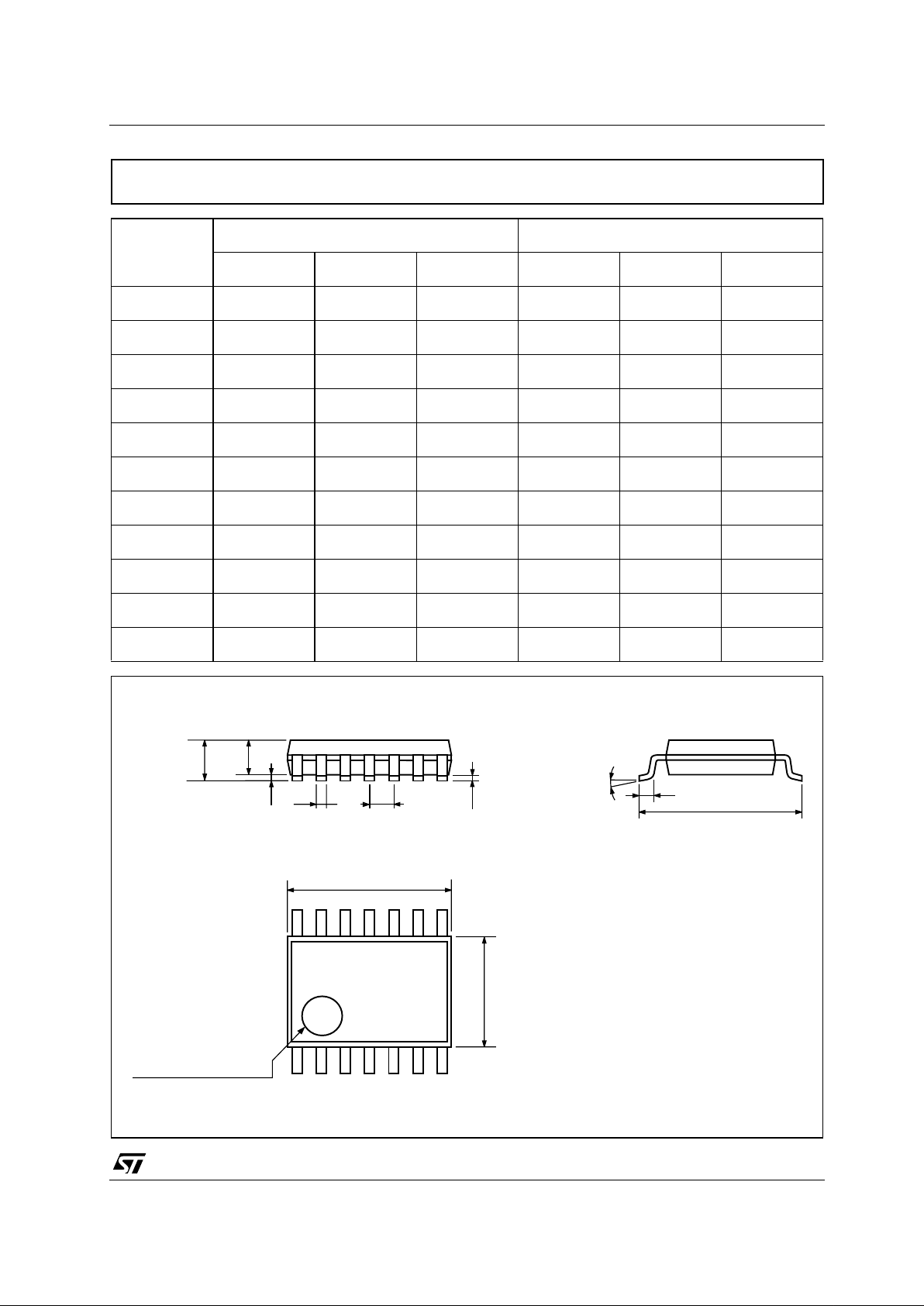
DIM.
mm. inch
MIN. TYP MAX. MIN. TYP. MAX.
A 1.75 0.068
a1 0.1 0.2 0.003 0.007
a2 1.65 0.064
b 0.35 0.46 0.013 0.018
b1 0.19 0.25 0.007 0.010
C 0.5 0.019
c1 45° (typ.)
D 8.55 8.75 0.336 0.344
E 5.8 6.2 0.228 0.244
e 1.27 0.050
e3 7.62 0.300
F 3.8 4.0 0.149 0.157
G 4.6 5.3 0.181 0.208
L 0.5 1.27 0.019 0.050
M 0.68 0.026
S8° (max.)
SO-14 MECHANICAL DATA
PO13G
Page 7
74LCX05
7/8
DIM.
mm. inch
MIN. TYP MAX. MIN. TYP. MAX.
A 1.2 0.047
A1 0.05 0.15 0.002 0.004 0.006
A2 0.8 1 1.05 0.031 0.039 0.041
b 0.19 0.30 0.007 0.012
c 0.09 0.20 0.004 0.0089
D 4.9 5 5.1 0.193 0.197 0.201
E 6.2 6.4 6.6 0.244 0.252 0.260
E1 4.3 4.4 4.48 0.169 0.173 0.176
e 0.65 BSC 0.0256 BSC
K0° 8°0° 8°
L 0.45 0.60 0.75 0.018 0.024 0.030
TSSOP14 MECHANICAL DATA
c
E
b
A2
A
E1
D
1
PIN 1 IDENTIFICATION
A1
L
K
e
0080337D
Page 8

74LCX05
8/8
Information furnished is bel ieved to be accurate and reliable. However, STMicroe lectronics assumes no responsibility for the
consequences of use of such information nor for any infringement of patents or other rights of third parties which may result from
its use. No li cense is granted by i mp lication or otherwise under a ny patent or patent rig hts of STMicroelectronics. Spec ificat ions
mentioned in this publication ar e subject to change without notice. This publication supersedes and replaces all information
previously supplied. S TMicroelectronics products are not authorized for use as critica l components in life suppo rt devices or
systems without express written approval of STMicroelectronics.
© The ST logo is a registered trademark of STMicroelectronics
© 2000 STM icroelectronics - Pr inted in Italy - All Rights Reserv ed
STMicr o el ectronics GROUP OF COMPA NI E S
Australi a - Brazil - Chi na - Finlan d - F rance - Germ any - Hong Kon g - India - Italy - Japan - Mal aysia - Malta - Morocco
Singapo re - Spain - Sweden - Swit zerland - Un i ted Kingdom
© http://www.st.com
 Loading...