

Page 1

查询74LCX05供应商
LOW VOLTAGE CMOS HEX INVERTER (OPEN DRAIN)
74LCX05
WITH 5V TOLERANT INPUTS
■ 5V TOLERANT INPUTS
■ HIGH SPEED:
t
= 5.2ns (MAX.) at VCC = 3V
PD
■ POWER DOWN PROTECTION ON INPUTS
AND OUTPUTS
■ SYMMETRICAL OUTPUT IMPEDANCE:
|I
| = IOL = 24mA (MIN) at VCC = 3V
OH
■ PCI BUS LEVELS GUARANTEED AT 24 mA
■ OPERATING VOLTAGE RANGE:
V
(OPR) = 2.0V to 3.6V (1.5V Data
CC
Retention)
■ PIN AND FUNCTION COMPATIBLE WITH
74 SERIES 05
■ LA TCH-UP PERFORMANCE EXCEEDS
500mA (JESD 17)
■ ESD PERFORMANCE:
HBM > 2000V (MIL STD 883 method 3015);
MM > 200V
DESCRIPTION
The 74LCX05 is a low voltage CMOS OPEN
DRAIN HEX INVERTER fabricated with
sub-micron silicon gate and double-layer metal
wiring C
2
MOS technology. It is ideal for low power
and high speed 3.3V applications. It can be
interfaced to 5V signal environment for inputs.
TSSOPSOP
Table 1: Order Codes
PACKAGE T & R
SOP 74LCX05MTR
TSSOP 74LCX05TTR
The internal circuit is composed of 3 stages
including buffer ou tput, whi ch provid es hig h no ise
immunity and stable output.
It has same speed performance at 3.3V than 5V
AC/ACT family, combined with a lower power
consumption.
All inputs and outputs are equipped with
protection circuits against static disc harge, giving
them 2KV ESD immunity and transient excess
voltage.
Figure 1: Pin C onnection And I EC Logic Symbol s
Rev. 3
1/11September 2004
Page 2

74LCX05
Figure 2: Input An d Output Equival e n t Ci rcui t
Table 2: Pin Description Table 3: Truth Table
PIN N° SYMBOL NAME AND FUNCTION
1, 3, 5, 9, 1 1,
13
2, 4, 6, 8, 10,
12
1A to 6A Data Inputs
1Y to 6Y Data Outputs
Z : High Impedance
AY
LZ
HL
7 GND Ground (0V)
14
V
CC
Positive Supply Voltage
Table 4: Absolute Maximum Ratings
Symbol Parameter Value Unit
V
V
V
V
I
I
OK
I
I
CC
I
GND
T
T
Absolute Maximum Ratings are those values beyond which damage to the device may occur. Functional operation under these conditions is
not implied
absolute maximum rating must be observed
1) I
O
2) VO < GND
Supply Voltage
CC
DC Input Voltage
I
DC Output Voltage (VCC = 0V)
O
DC Output Voltage (High or Low State) (note 1) -0.5 to VCC + 0.5
O
DC Input Diode Current
IK
DC Output Diode Current (note 2)
DC Output Current
O
DC Supply Current per Supply Pin
DC Ground Current per Supply Pin
Storage Temperature
stg
Lead Temperature (10 sec)
L
-0.5 to +7.0 V
-0.5 to +7.0 V
-0.5 to +7.0 V
V
- 50 mA
- 50 mA
± 50 mA
± 100 mA
± 100 mA
-65 to +150 °C
300 °C
2/11
Page 3

74LCX05
Table 5: Recommended Operating Conditions
Symbol Parameter Value Unit
V
V
V
V
I
OH
I
OH
T
dt/dv Input Rise and Fall Time (note 2) 0 to 10 ns/V
1) Truth T abl e guarante ed: 1.5V to 3.6V
2) V
from 0.8V to 2V at VCC = 3.0V
IN
Table 6: DC Specifications
Supply Voltage (note 1)
CC
Input Voltage
I
Output Voltage (VCC = 0V)
O
Output Voltage (High or Low State) 0 to V
O
, I
High or Low Level Output Current (VCC = 3.0 to 3.6V)
OL
, I
High or Low Level Output Current (VCC = 2.7V)
OL
Operating Temperature
op
Test Condition Value
2.0 to 3.6 V
0 to 5.5 V
0 to 5.5 V
CC
± 24 mA
± 12 mA
-55 to 125 °C
V
Symbol Parameter
V
CC
(V)
V
V
V
I
I
OZ
I
CC
∆I
High Level Input
IH
Voltage
Low Level Input
IL
Voltage
Low Level Output
OL
Voltage
Input Leakage
I
I
Current
Power Off Leakage
off
Current
High Impedance
Output Leakage
Current
Quiescent Supply
Current
ICC incr. per Input
CC
2.7 to 3.6
2.7 to 3.6
2.7
3.0
2.7 to 3.6
0
2.7 to 3.6
2.7 to 3.6
2.7 to 3.6
IO=100 µA
I
O
I
O
I
O
V
= 0 to 5.5V
I
or VO = 5.5V
V
I
= VIH or V
V
I
VO = 0 to V
VI = VCC or GND
V
or VO= 3.6 to 5.5V
I
VIH = VCC - 0.6V
Table 7: Dynamic Switching Characteristics
-40 to 85 °C -55 to 125 °C
Min. Max. Min. Max.
2.0 2.0 V
0.8 0.8 V
0.2 0.2
=12 mA
=16 mA
=24 mA
0.4 0.4
0.4 0.4
0.55 0.55
± 5 ± 5 µA
10 10 µA
IL
CC
± 5 ± 5 µA
10 10
± 10 ± 10
500 500 µA
Test Condition Value
Unit
V
µA
= 25 °C
Symbol Parameter
V
CC
(V)
V
OLP
V
OLV
1) Number of outputs defined as "n". Measured wi t h "n-1" output s switching from HIGH to LO W or LOW to HIGH. The remaining output is
measur ed i n the LOW state.
Dynamic Low Level Quiet
Output (note 1)
3.3
V
V
IH
= 0V
IL
= 3.3V
T
A
Min. Typ. Max.
0.8
-0.8
Unit
V
3/11
Page 4

74LCX05
Table 8: AC Electrical Characteristics
Test Condition Value
Symbol Parameter
V
CC
(V)
t
PLZ
t
PZL
t
OSLH
t
OSHL
1) Skew is defined as the absolute value of the difference between the actual propagation delay for any two outputs of the same device switching in the sa me directio n, either HIGH or LOW (t
2) Param eter guaran teed by design
Propagation Delay
Time
Propagation Delay
Time
Output To Output
Skew Time (note1,
2)
2.7
3.0 to 3.6 1.0 5.2 1.0 5.2
2.7
3.0 to 3.6 1.0 5.2 1.0 5.2
3.0 to 3.6 50 500 2.5 1.0 1.0 ns
OSLH
C
L
(pF)
50 500 2.5
50 500 2.5
= | t
PLHm
- t
R
(Ω)
PLHn
|, t
L
OSHL
t
s
(ns)
= t
= | t
-40 to 85 °C -55 to 125 °C
r
Min. Max. Min. Max.
6.5 6.5
6.5 6.5
- t
PHLn
|)
PHLm
Unit
ns
ns
Table 9: Capacitive Characteristics
Test Condition Value
= 25 °C
Symbol Parameter
V
CC
(V)
C
C
OUT
C
1) CPD is defined as the value of the IC’s internal equivalent capacitance which is calculated from the operating current consumption without
load. (Refer to Test Circuit). Average operating current can be obtained by the following equation. I
Input Capacitance
IN
Output Capacitance
Power Dissipation Capacitance
PD
(note 1)
3.3
3.3
VIN = 0 to V
VIN = 0 to V
3.3 fIN = 10MHz
V
= 0 or V
IN
CC
CC
CC
T
A
Min. Typ. Max.
6pF
14 pF
5
= CPD x VCC x fIN + ICC/6 (per gate)
CC(opr)
Unit
pF
Figure 3: Test Circuit
TEST SWITCH
, t
t
PLH
PHL
, t
t
PZL
PLZ
, t
t
PZH
PHZ
CL = 50 pF or equivalent (includes jig and probe capacitance)
RL = R1 = 500Ω or equivalent
= Z
R
of pulse generator (typically 50Ω)
T
OUT
4/11
Open
6V
GND
Page 5
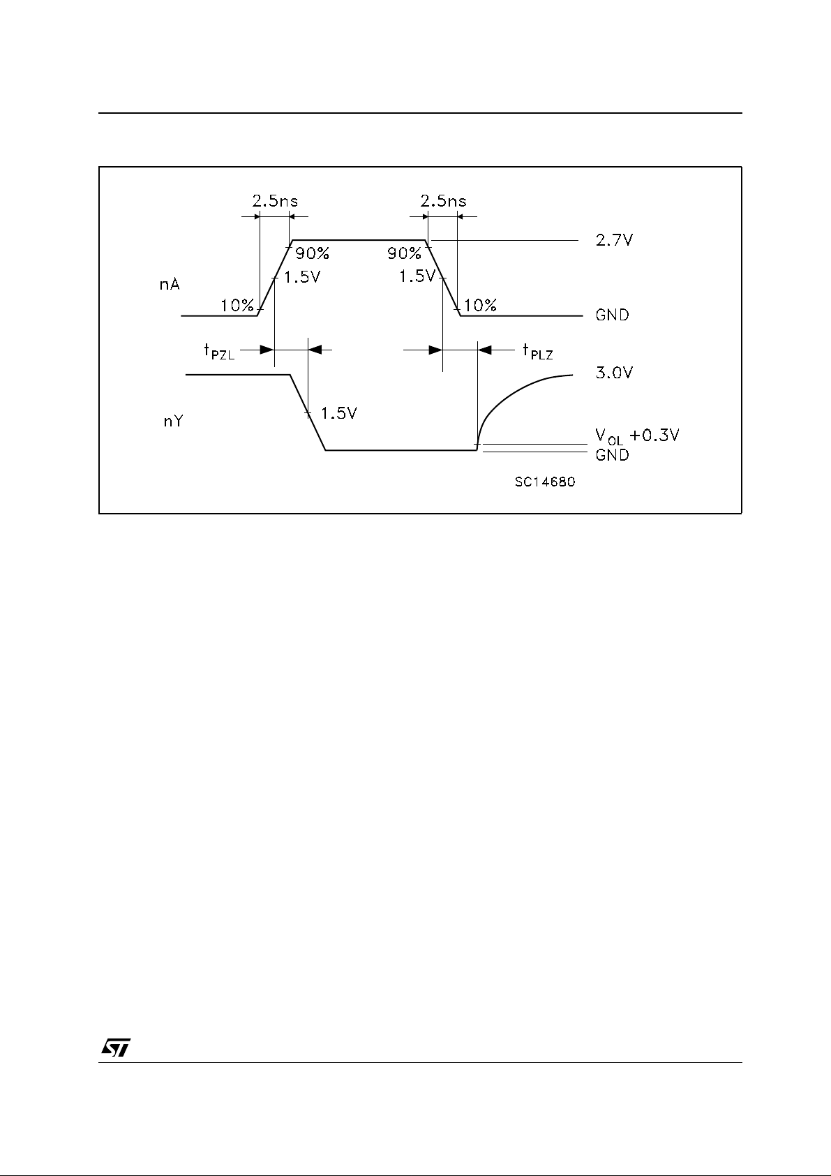
Figure 4: Waveform - Propagation Delay (f=1MHz; 50% duty cycle)
74LCX05
5/11
Page 6
74LCX05
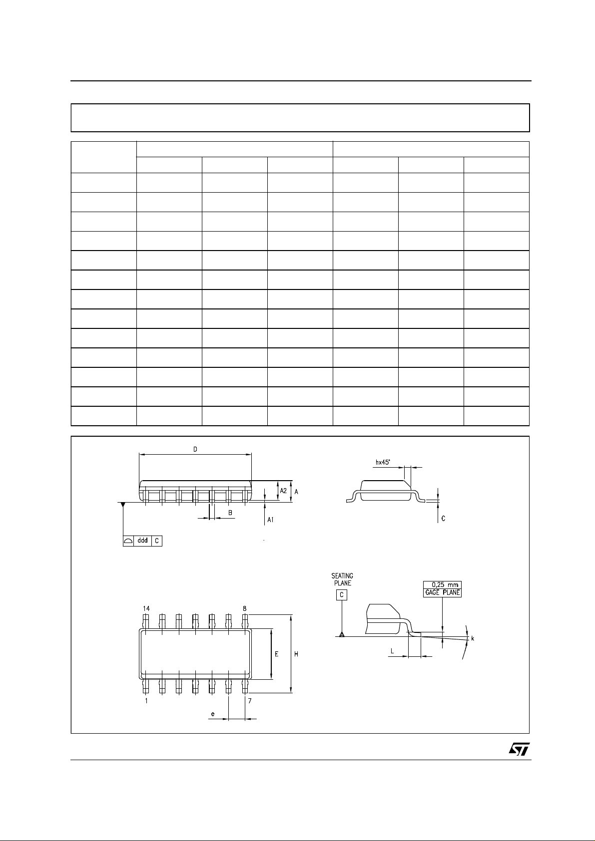
SO-14 MECHANICAL DATA
DIM.
A 1.35 1.75 0.053 0.069
A1 0.1 0.25 0.004 0.010
A2 1.10 1.65 0.043 0.065
B 0.33 0.51 0.013 0.020
C 0.19 0.25 0.007 0.010
D 8.55 8.75 0.337 0.344
E 3.8 4.0 0.150 0.157
e 1.27 0.050
H 5.8 6.2 0.228 0.244
h 0.25 0.50 0.010 0.020
L 0.4 1.27 0.016 0.050
k0° 8° 0° 8°
ddd 0.100 0.004
MIN. TYP MAX. MIN. TYP. MAX.
mm. inch
6/11
0016019D
Page 7
74LCX05
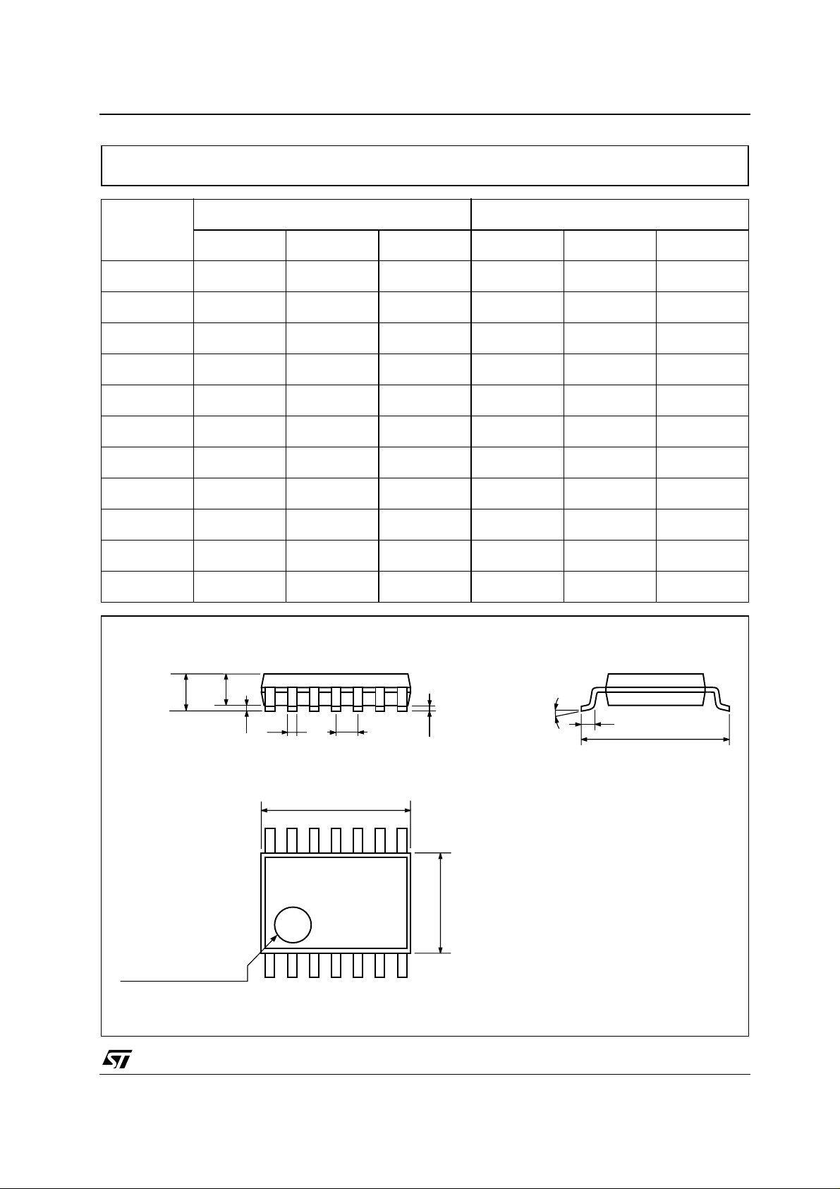
TSSOP14 MECHANICAL DATA
mm. inch
DIM.
MIN. TYP MAX. MIN. TYP. MAX.
A 1.2 0.047
A1 0.05 0.15 0.002 0.004 0.006
A2 0.8 1 1.05 0.031 0.039 0.041
b 0.19 0.30 0.007 0.012
c 0.09 0.20 0.004 0.0089
D 4.9 5 5.1 0.193 0.197 0.201
E 6.2 6.4 6.6 0.244 0.252 0.260
E1 4.3 4.4 4.48 0.169 0.173 0.176
e 0.65 BSC 0.0256 BSC
K0˚ 8˚0˚ 8˚
L 0.45 0.60 0.75 0.018 0.024 0.030
A2
A
A1
b
e
c
K
L
E
D
E1
PIN 1 IDENTIFICATION
1
0080337D
7/11
Page 8
74LCX05
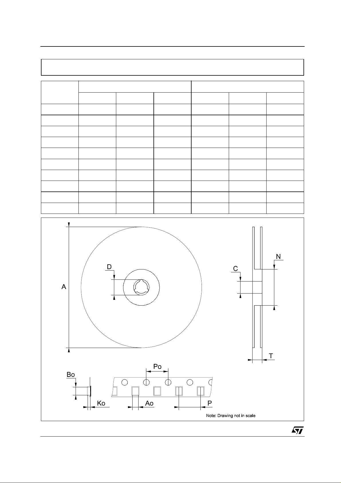
Tape & Reel SO-14 MECHANICAL DATA
mm. inch
DIM.
MIN. TYP MAX. MIN. TYP. MAX.
A 330 12.992
C 12.8 13.2 0.504 0.519
D 20.2 0.795
N 60 2.362
T 22.4 0.882
Ao 6.4 6.6 0.252 0.260
Bo 9 9.2 0.354 0.362
Ko 2.1 2.3 0.082 0.090
Po 3.9 4.1 0.153 0.161
P 7.9 8.1 0.311 0.319
8/11
Page 9

74LCX05
Tape & Reel TSSOP14 MECHANICAL DATA
mm. inch
DIM.
MIN. TYP MAX. MIN. TYP. MAX.
A 330 12.992
C 12.8 13.2 0.504 0.519
D 20.2 0.795
N 60 2.362
T 22.4 0.882
Ao 6.7 6.9 0.264 0.272
Bo 5.3 5.5 0.209 0.217
Ko 1.6 1.8 0.063 0.071
Po 3.9 4.1 0.153 0.161
P 7.9 8.1 0.311 0.319
9/11
Page 10
74LCX05
Table 10: Revision History
Date Revision Description of Change s
15-Sep-2004 3 Ordering Codes Revision - pag. 1.
10/11
Page 11

74LCX05
Information furnished is believed to be accurate and reliable. However, STMicroelectronics assumes no responsibility for the consequences
of use of s uch inf ormati on nor for a ny infr ing eme nt o f p atent s or o ther ri ghts of third parti es wh ich m ay res ult fr om i ts us e. No li cens e i s gr an ted
by implication or otherwise under any patent or patent rights of STMicroelectronics. Specifications mentioned in this publication are subject
to change without notice. This publication supersedes and replaces all information previously supplied. STMicroelectronics products are not
authorized for use as critical components in life support devices or systems without express written approval of STMicroelectronics.
The ST logo is a registered trademark of STMicroelectronics
All other names are the property of their respective owners
© 2004 STMicroelectronics - All Rights Reserved
STMicroelectronics group of companies
Australia - Belgium - Brazil - Canada - China - Czech Republic - Finland - France - Germany - Hong Kong - India - Israel - Italy - Japan -
Malaysia - Malta - Morocco - Singapore - Spain - Sweden - Switzerland - United Kingdom - United States of America
www.st.com
11/11
 Loading...