

Datasheet 74LCX04CW, 74LCX04SJX, 74LCX04SJ, 74LCX04MX, 74LCX04MTCX Datasheet (Fairchild Semiconductor)
...Page 1
March 1995
Revised May 1999
74LCX04 Low Voltage Hex Inverter with 5V Tolerant Inputs
© 1999 Fairchild Semiconductor Corporation DS012410.prf www.fairchildsemi.com
74LCX04
Low Voltage Hex Inverter with 5V Tolerant Inputs
General Description
The LCX04 contains six in verters. The i nputs toler ate voltages up to 7V allowing the interface of 5V systems to 3V
systems.
The 74LCX04 is fabricated with advanced CMO S technology to achieve high speed operation while maintaining
CMOS low power dissipation.
Features
■ 5V tolerant inputs
■ 2.3V–3.6V V
CC
specifications provided
■ 5.2 ns t
PD
max (V
CC
= 3.3V), 10 µA ICC max
■ Power down high impedance inputs and outputs
■ ±24 mA output drive (V
CC
= 3.0V)
■ Implements patented noise/EMI reduction circuitry
■ Latch-up performance exceeds 500 mA
■ ESD performance:
Human body model > 2000V
Machine model > 200V
Ordering Code:
Devices also availab le in Tape and Reel. Specify by appending th e s uffix let t er “X” to the ordering code.
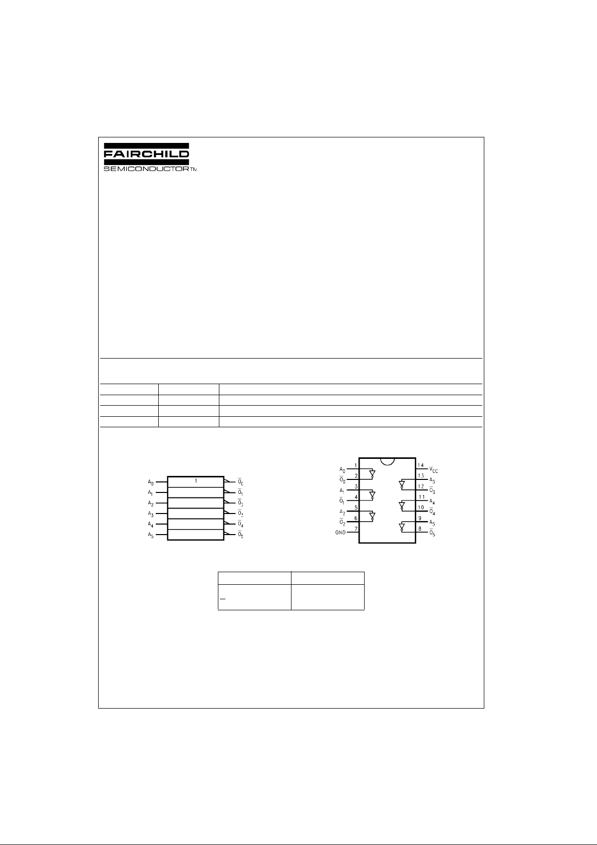
Logic Symbol
IEEE/IEC
Connection Diagram
Pin Descriptions
Order Number Package Number Package Description
74LCX04M M14A 14-Lead Small Outline Integrated Circuit (SOIC), JEDEC MS-120, 0.150” Narrow
74LCX04SJ M14D 14-Lead Small Outline Package (SOP), EIAJ TYPE II, 5.3mm Wide
74LCX04MTC MTC14 14-Lead Thin Shrink Small Outline Package (TSSOP), JEDEC MO-153, 4.4mm Wide
Pin Names Description
A
n
Inputs
O
n
Outputs
Page 2
www.fairchildsemi.com 2
74LCX04
Absolute Maximum Ratings(Note 1)
Recommended Operating Conditions (Note 3)
Note 1: The Absolute Maximum Ratings are those values beyond which the safety of the device cannot be guaranteed. The device should not be operated
at these limits. Th e parametric values def ined in the Electrical Cha racteristic s tables are not guaran teed at the A bsolute Ma ximum Rating s. The “Rec ommended Operat ing Conditions” table will define the conditions fo r ac t ual device operation.
Note 2: I
O
Absolute Maximum Rating must be observed.
Note 3: Unused inputs must be held HIGH or LOW. They may not float.
DC Electrical Characteristics
Symbol Parameter Value Conditions Units
V
CC
Supply Voltage −0.5 to +7.0 V
V
I
DC Input Voltage −0.5 to +7.0 V
V
O
DC Output Voltage −0.5 to VCC + 0.5 Output in HIGH or LOW State (Note 2) V
I
IK
DC Input Diode Current −50 VI < GND mA
I
OK
DC Output Diode Current −50 VO < GND
mA
+50 V
O
> V
CC
I
O
DC Output Source/Sink Current ±50 mA
I
CC
DC Supply Current per Supply Pin ±100 mA
I
GND
DC Ground Cu rrent per Ground Pin ±100 mA
T
STG
Storage Temperature −65 to +150 °C
Symbol Parameter Min Max Units
V
CC
Supply Voltage Operating 2 .0 3.6
V
Data Retention 1.5 3.6
V
I
Input Voltage 05.5V
V
O
Output Voltage HIGH or LOW State 0 V
CC
V
I
OH/IOL
Output Current VCC = 3.0V − 3.6V ±24
mA
V
CC
= 2.7V − 3.0V ±12
V
CC
= 2.3V − 2.7V ±8
T
A
Free-Air Operating Temperature −40 85 °C
∆t/∆V Input Edge Rate, V
IN
= 0.8V–2.0V, VCC = 3.0V 0 10 ns/V
Symbol Parameter Conditions
V
CCTA
= −40°C to +85°C
Units
(V) Min Max
V
IH
HIGH Level Input Voltage 2.3 − 2.7 1.7
V
2.7 − 3.6 2.0
V
IL
LOW Level Input Voltage 2.3 − 2.7 0.7
V
2.7 − 3.6 0.8
V
OH
HIGH Level Output Voltage IOH = −100 µA2.3 − 3.6 VCC − 0.2
IOH = −8 mA 2.3 1.8
IOH = −12 mA 2.7 2.2
V
IOH = −18 mA 3.0 2.4
IOH = 24 mA 3.0 2.2
V
OL
LOW Level Output Voltage IOL = −100 µA2.3 − 3.6 0.2
IOL = 8 mA 2.3 0.6
V
IOL = 12 mA 2.7 0.4
IOL = 16 mA 3.0 0.4
IOL = 24 mA 3.0 0.55
I
I
Input Leakage Current 0 ≤ VI ≤ 5.5V 2.3 − 3.6 ±5.0 µA
I
OFF
Power-Off Leakage Current VI or VO = 5.5V 0 10 µA
I
CC
Quiescent Supply Current VI = VCC or GND 2.3 − 3.6 10
µA
3.6V ≤ VI ≤ 5.5V 2.3 − 3.6 ±10
∆I
CC
Increase in ICC per Input VIH = VCC −0.6V 2.3 − 3.6 500 µA
Page 3
3 www.fairchildsemi.com
74LCX04
AC Electrical Characteristics
Note 4: Skew is def ined as the absolut e v alue of the difference between the actual propagation delay for any two separate outputs of the same device. The
specification applies t o any outputs switching in th e s am e direction, either HIG H -t o-LOW (t
OSHL
) or LOW-to-HIGH (T
OSLH
).
Dynamic Switching Characteristics
Capacitance
Symbol Parameter
TA = −40°C to +85°C, RL = 500Ω
Units
VCC = 3.3V ± 0.3V VCC = 2.7V VCC = 2.5V ± 0.2V
CL= 50 pF CL = 50 pF CL=30 pF
Min Max Min Max Min Max
t
PHL
Propagation Delay Time 1.5 5.2 1.5 6.0 1.5 6.2
ns
t
PLH
1.5 5.2 1.5 6.0 1.5 6 .2
t
OSHL
Output to Output Skew 1.0
ns
t
OSLH
(Note 4) 1.0
Symbol Parameter Conditions
V
CC
(V)
TA = 25°C
Units
Typical
V
OLP
Quiet Output Dynamic Peak V
OL
CL = 50 pF, VIH = 3.3V, VIL = 0V 3.3 0.8
V
CL = 30 pF, VIH = 2.5V, VIL = 0V 2.5 0.6
V
OLV
Quiet Output Dynamic Valley V
OL
CL = 50 pF, VIH = 3.3V, VIL = 0V 3.3 −0.8
V
CL = 30 pF, VIH = 2.5V, VIL = 0V 2.5 −0.6
Symbol Parameter Conditions Typical Units
C
IN
Input Capacitance VCC = Open, VI = 0V or V
CC
7pF
C
OUT
Output Capacitance VCC = 3.3V, VI = 0V or V
CC
8pF
C
PD
Power Dissipation Capacitance VCC = 3.3V, VI = 0V or VCC, f = 10 MHz 25 pF
Page 4

www.fairchildsemi.com 4
74LCX04
AC Loading and Waveforms Generic for LCX Family
FIGURE 1. AC Test Circuit
(C
L
includes probe and jig capacitance)
Waveform for Inverting and Non-Inverting Functions
Propagation Delay, Pulse Width and t
rec
Waveforms
3-STATE Output High Enable and
Disable TImes for Logic
3-STATE Output Low Enable a nd
Disable Times for Logic
Setup Time, H old TIme and Recove ry TIme for Logic
t
rise
and t
fall
FIGURE 2. Waveforms
(Input Pulse Characteristics; f=1MHz, t
r=tf
=3ns)
Test Switch
t
PLH
, t
PHL
Open
t
PZL
, t
PLZ
6V at VCC = 3.3 ± 0.3V
V
CC
x 2 at VCC = 2.5 ± 0.2V
t
PZH,tPHZ
GND
Symbol
V
CC
3.3V ± 0.3V 2.7V 2.5V ± 0.2V
V
mi
1.5V 1.5V VCC/2
V
mo
1.5V 1.5V VCC/2
V
x
VOL + 0.3V VOL + 0.3V VOL + 0.15V
V
y
VOH − 0.3V VOH − 0.3V VOH − 0.15V
Page 5

5 www.fairchildsemi.com
74LCX04
Schematic Diagram Generic for LCX Family
Page 6

www.fairchildsemi.com 6
74LCX04
Physical Dimensions inches (millimeters) unless otherwise noted
14-Lead Small Outline Integrated Circuit (SOIC), JEDEC MS-120, 0.150” Narrow
Package Number M14A
14-Lead Small Outline Package (SOP), EIAJ TYPE II, 5.3mm Wide
Package Number M14D
Page 7

Fairchild does not assume any responsibility for use of any circuitry described, no circuit patent licenses are implied and Fairchild reserves the right at any time without notice to change said circuitry and specifications.
74LCX04 Low Voltage Hex Inverter with 5V Tolerant Inputs
LIFE SUPPORT POLICY
FAIRCHILD’S PRODUCTS ARE NOT AUTHORIZED FOR USE AS CRITICAL COMPONENTS IN LIFE SUPPORT
DEVICES OR SYSTEMS WITHOUT THE EXPRESS WRITTEN APPROVAL OF THE PRESIDENT OF FAIRCHILD
SEMICONDUCTOR CORPORATION. As used herein:
1. Life support devices or systems are dev ic es or syste ms
which, (a) are intended for surgical implant into the
body, or (b) support or sustain life, and (c) whose failure
to perform when properly used in accordance with
instructions for use provided i n the labe li ng, can be re asonably expected to result in a significant injury to the
user.
2. A critical componen t in any com ponent o f a l ife supp ort
device or system whose failu re to perform can b e reasonably expected to c ause th e fa i lure of the li fe s upp or t
device or system, or to affect its safety or effectiveness.
www.fairchildsemi.com
Physical Dimensions inches (millimeters) unless otherwise noted (Continued)
14-Lead Thin Shrink Small Outline Package (TSSOP), JEDEC MO-153, 4.4mm Wide
Package Number MTC14
 Loading...