

Page 1
INTEGRATED CIRCUITS
DATA SH EET
For a complete data sheet, please also download:
•The IC06 74HC/HCT/HCU/HCMOS Logic Family Specifications
74HC/HCT74
Dual D-type flip-flop with set and
reset; positive-edge trigger
Product specification
Supersedes data of September 1993
File under Integrated Circuits, IC06
1998 Feb 23
Page 2
Philips Semiconductors Product specification
Dual D-type flip-flop with set and reset;
positive-edge trigger
FEATURES
• Output capability: standard
• ICC category: flip-flops
GENERAL DESCRIPTION
The 74HC/HCT74 are high-speed Si-gate CMOS devices
and are pin compatible with low power Schottky TTL
(LSTTL). They are specified in compliance with JEDEC
standard no. 7A.
The 74HC/HCT74 are dual positive-edge triggered, D-type
flip-flops with individual data (D) inputs, clock (CP) inputs,
set (
SD) and reset (RD) inputs; also complementary Q and
Q outputs.
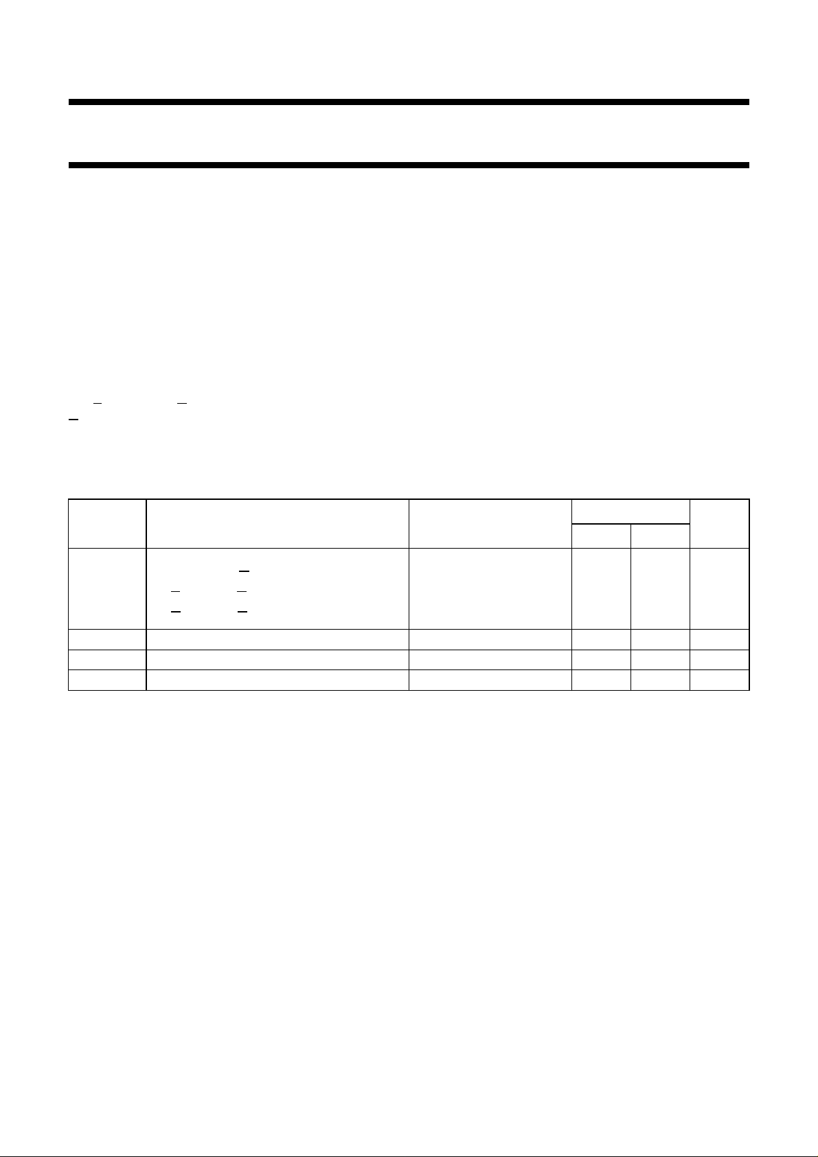
QUICK REFERENCE DATA
GND = 0 V; T
= 25 °C; tr= tf= 6 ns
amb
SYMBOL PARAMETER CONDITIONS
t
/ t
PHL
PLH
f
max
C
I
C
PD
propagation delay CL= 15 pF; VCC= 5 V
nCP to nQ, n
n
S
to nQ, nQ1518ns
D
n
R
to nQ, nQ1618ns
D
Q1415ns
maximum clock frequency 76 59 MHz
input capacitance 3.5 3.5 pF
power dissipation capacitance per flip-flop notes 1 and 2 24 29 pF
The set and reset are asynchronous active LOW inputs
and operate independently of the clock input. Information
on the data input is transferred to the Q output on the
LOW-to-HIGH transition of the clock pulse. The D inputs
must be stable one set-up time prior to the LOW-to-HIGH
clock transition for predictable operation.
Schmitt-trigger action in the clock input makes the circuit
highly tolerant to slower clock rise and fall times.
74HC/HCT74
TYPICAL
UNIT
HC HCT
Notes
1. C
is used to determine the dynamic power dissipation (PDin µW):
PD
PD= CPD× V
2
× fi+∑(CL× V
CC
2
× fo) where:
CC
fi= input frequency in MHz
fo= output frequency in MHz
∑ (CL× V
2
× fo) = sum of outputs
CC
CL= output load capacitance in pF
VCC= supply voltage in V
2. For HC the condition is VI= GND to V
CC
For HCT the condition is VI= GND to VCC− 1.5 V
1998 Feb 23 2
Page 3
Philips Semiconductors Product specification
Dual D-type flip-flop with set and reset;
74HC/HCT74
positive-edge trigger
ORDERING INFORMATION
TYPE
NUMBER
74HC(T)74N DIP14 plastic dual in-line package; 14 leads (300 mil) SOT27-1
74HC(T)74D SO14 plastic small outline package; 14 leads; body width 3.9 mm SOT108-1
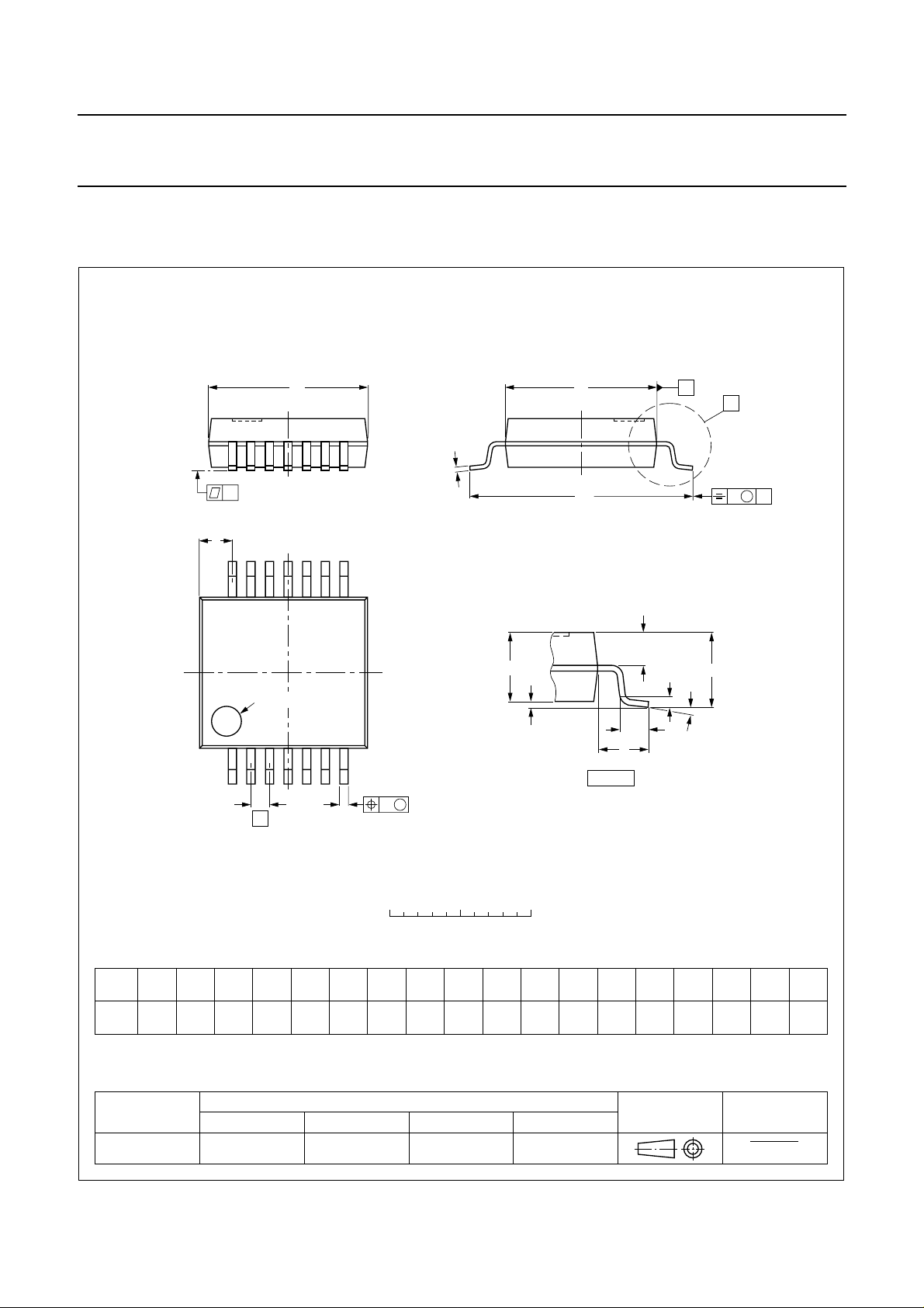
74HCT74DB SSOP14 plastic shrink small outline package; 14 leads; body width 5.3 mm SOT337-1
74HCT74PW TSSOP14 plastic thin shrink small outline package; 14 leads; body width 4.4 mm SOT402-1
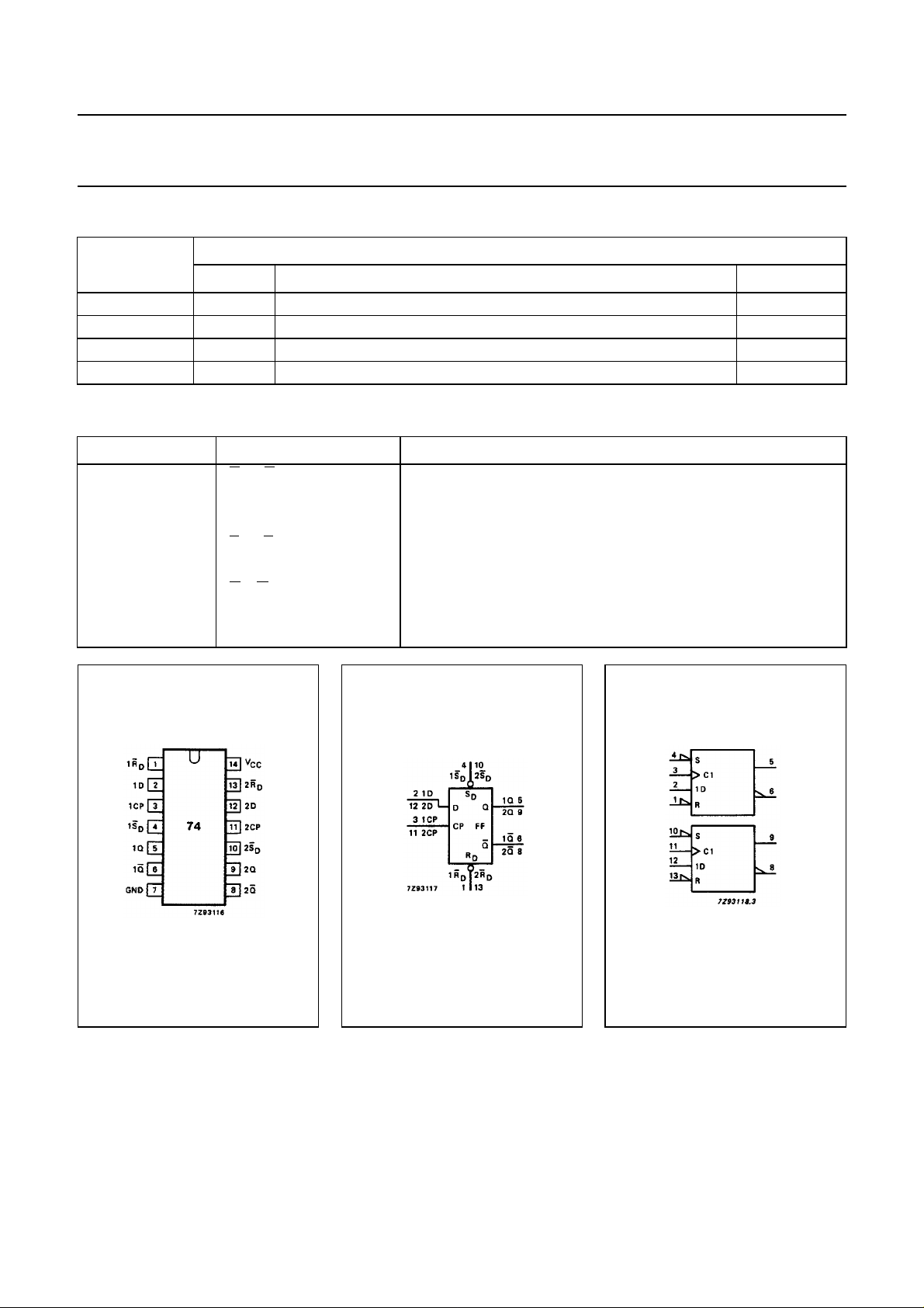
PIN DESCRIPTION
PIN NO. SYMBOL NAME AND FUNCTION
1, 13 1
2, 12 1D, 2D data inputs
3, 11 1CP, 2CP clock input (LOW-to-HIGH, edge-triggered)
4, 10 1
5, 9 1Q, 2Q true flip-flop outputs
6, 8 1
7 GND ground (0 V)
14 V
NAME DESCRIPTION VERSION
RD, 2R
D
SD, 2S
D
Q, 2Q complement flip-flop outputs
CC
asynchronous reset-direct input (active LOW)
asynchronous set-direct input (active LOW)
positive supply voltage
PACKAGE
Fig.1 Pin configuration. Fig.2 Logic symbol. Fig.3 IEC logic symbol.
1998 Feb 23 3
Page 4
Philips Semiconductors Product specification
Dual D-type flip-flop with set and reset;
positive-edge trigger
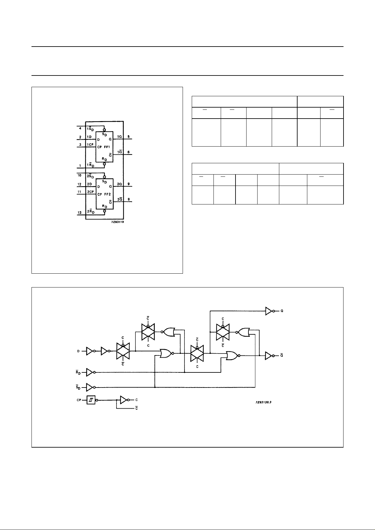
Fig.4 Functional diagram.
74HC/HCT74
FUNCTION TABLE
INPUTS OUTPUTS
S
D
LHXXHL
HLXXLH
LLXXHH
S
D
HH↑LL H
HH↑HH L
Note
1. H = HIGH voltage level
L = LOW voltage level
X = don’t care
↑ = LOW-to-HIGH CP transition
Q
n+1
R
D
CP D Q Q
INPUTS OUTPUTS
R
CP D Q
D
n+1
Q
n+1
= state after the next LOW-to-HIGH CP transition
Fig.5 Logic diagram (one flip-flop).
1998 Feb 23 4
Page 5

Philips Semiconductors Product specification
Dual D-type flip-flop with set and reset;
positive-edge trigger
DC CHARACTERISTICS FOR 74HC
For the DC characteristics see
Output capability: standard
ICCcategory: flip-flops
AC CHARACTERISTICS
GND = 0 V; t
= tf= 6 ns; CL= 50 pF
r
SYMBOL PARAMETER
t
PHL
/ t
propagation delay
PLH
nCP to nQ, nQ
t
PHL
/ t
propagation delay
PLH
nSDto nQ, nQ
t
PHL
/ t
propagation delay
PLH
nRDto nQ, nQ
t
THL
t
W
/ t
output transition time 19 75 95 110 ns 2.0 Fig.6
TLH
clock pulse width
HIGH or LOW
t
W
set or reset pulse width
LOW
t
rem
removal time
set or reset
t
su
set-up time
nD to nCP
t
h
hold time
nCP to nD
f
max
maximum clock pulse
frequency
“74HC/HCT/HCU/HCMOS Logic Family Specifications”
min. typ. max. min. max min. max.
47 175 220 265 ns 2.0 Fig.6
17 35 44 53 4.5
14 30 37 45 6.0
50 200 250 300 ns 2.0 Fig.7
18 40 50 60 4.5
14 34 43 51 6.0
52 200 250 300 ns 2.0 Fig.7
19 40 50 60 4.5
15 34 43 51 6.0
7 15 19 22 4.5
6 13 16 19 6.0
80 19 100 120 ns 2.0 Fig.6
16 7 20 24 4.5
14 6 17 20 6.0
80 19 100 120 ns 2.0 Fig.7
16 7 20 24 4.5
14 6 17 20 6.0
30 3 40 45 ns 2.0 Fig.7
6 1 8 9 4.5
5 1 7 8 6.0
60 6 75 90 ns 2.0 Fig.6
12 2 15 18 4.5
10 2 13 15 6.0
3 −6 3 3 ns 2.0 Fig.6
3 −2 3 3 4.5
3 −2 3 3 6.0
6.0 23 4.8 4.0 MHz 2.0 Fig.6
30 69 24 20 4.5
35 82 28 24 6.0
T
amb
74HC
(°C)
.
UNIT
74HC/HCT74
TEST CONDITIONS
V
CC
WAVEFORMS+25 −40 to +85 −40 to +125
(V)
1998 Feb 23 5
Page 6

Philips Semiconductors Product specification
Dual D-type flip-flop with set and reset;
74HC/HCT74
positive-edge trigger
DC CHARACTERISTICS FOR 74HCT
For the DC characteristics see
Output capability: standard
ICCcategory: flip-flops
Note to HCT types
The value of additional quiescent supply current (∆I
To determine ∆ICC per input, multiply this value by the unit load coefficient shown in the table below.
INPUT UNIT LOAD COEFFICIENT
nD 0.70
nR
n
D
S
D
0.70
0.80
nCP 0.80
AC CHARACTERISTICS FOR 74HCT
GND = 0 V; t
= tf= 6 ns; CL= 50 pF
r
“74HC/HCT/HCU/HCMOS Logic Family Specifications”
) for a unit load of 1 is given in the family specifications.
CC
.
SYMBOL PARAMETER
t
PHL
/ t
propagation delay
PLH
nCP to nQ, nQ
t
PHL
/ t
propagation delay
PLH
nSDto nQ, nQ
t
PHL
/ t
propagation delay
PLH
nRDto nQ, nQ
t
THL
t
W
/ t
output transition time 7 15 19 22 ns 4.5 Fig.6
TLH
clock pulse width
HIGH or LOW
t
W
set or reset pulse width
LOW
t
rem
removal time
set or reset
t
su
set-up time
nD to nCP
t
h
hold time
nCP to nD
f
max
maximum clock pulse
frequency
T
amb
(°C)
TEST CONDITIONS
74HCT
UNIT
V
(V)
CC
WAVEFORMS+25 −40 to +85 −40 to +125
min. typ. max. min. max. min. max.
18 35 44 53 ns 4.5 Fig.6
23 40 50 60 ns 4.5 Fig.7
24 40 50 60 ns 4.5 Fig.7
18 9 23 27 ns 4.5 Fig.6
16 9 20 24 ns 4.5 Fig.7
6 1 8 9 ns 4.5 Fig.7
12 5 15 18 ns 4.5 Fig.6
3 −3 3 3 ns 4.5 Fig.6
27 54 22 18 MHz 4.5 Fig.6
1998 Feb 23 6
Page 7

Philips Semiconductors Product specification
Dual D-type flip-flop with set and reset;
positive-edge trigger
AC WAVEFORMS
The shaded areas indicate when the input is permitted to
change for predictable output performance.
(1) HC : V
HCT: V
= 50%; VI= GND to VCC.
M
= 1.3 V; VI= GND to 3 V.
M
74HC/HCT74
Fig.6 Waveforms showing the clock (nCP) to output (nQ, nQ) propagation delays, the clock pulse width, the nD
to nCP set-up, the nCP to nD hold times, the output transition times and the maximum clock pulse
frequency.
(1) HC : VM= 50%; VI= GND to VCC.
HCT: V
= 1.3 V; VI= GND to 3 V.
M
handbook, full pagewidth
nCP INPUT
nSD INPUT
nRD INPUT
nQ OUTPUT
nQ OUTPUT
t
V
PLH
t
M
PHL
(1)
t
t
W
(1)
V
M
(1)
V
M
rem
t
V
PLH
M
t
PHL
t
W
(1)
(1)
V
M
t
rem
MGL350
Fig.7 Waveforms showing the set (nSD) and reset (nRD) input to output (nQ, nQ) propagation delays, the set
and reset pulse widths and the nRD, nSDto nCP removal time.
1998 Feb 23 7
Page 8

Philips Semiconductors Product specification
Dual D-type flip-flop with set and reset;
positive-edge trigger
PACKAGE OUTLINES
DIP14: plastic dual in-line package; 14 leads (300 mil)
D
seating plane
L
Z
14
e
b
74HC/HCT74
SOT27-1
M
E
A
2
A
A
1
w M
b
1
8
c
(e )
1
M
H
pin 1 index
1
0 5 10 mm
DIMENSIONS (inch dimensions are derived from the original mm dimensions)
A
A
A
UNIT
inches
Note
1. Plastic or metal protrusions of 0.25 mm maximum per side are not included.
max.
mm
OUTLINE
VERSION
SOT27-1
1 2
min.
max.
1.73
1.13
0.068
0.044
IEC JEDEC EIAJ
050G04 MO-001AA
b
b
1
0.53
0.38
0.021
0.015
0.36
0.23
0.014
0.009
REFERENCES
cD
scale
(1) (1)
19.50
18.55
0.77
0.73
7
Ee M
6.48
6.20
0.26
0.24
E
(1)
Z
L
e
1
3.60
3.05
0.14
0.12
M
E
8.25
7.80
0.32
0.31
EUROPEAN
PROJECTION
10.0
8.3
0.39
0.33
H
0.2542.54 7.62
ISSUE DATE
w
0.010.10 0.30
92-11-17
95-03-11
max.
2.24.2 0.51 3.2
0.0870.17 0.020 0.13
1998 Feb 23 8
Page 9

Philips Semiconductors Product specification
Dual D-type flip-flop with set and reset;
positive-edge trigger
SO14: plastic small outline package; 14 leads; body width 3.9 mm
D
c
y
Z
14
8
74HC/HCT74
SOT108-1
E
H
E
A
X
v M
A
pin 1 index
1
e
0 2.5 5 mm
DIMENSIONS (inch dimensions are derived from the original mm dimensions)
UNIT
mm
inches
Note
1. Plastic or metal protrusions of 0.15 mm maximum per side are not included.
A
max.
1.75
0.069
A
1
0.25
0.10
0.010
0.004
A2A3b
1.45
0.25
1.25
0.057
0.01
0.049
p
0.49
0.36
0.019
0.014
0.25
0.19
0.0100
0.0075
(1)E(1)
cD
8.75
8.55
0.35
0.34
7
w M
b
p
scale
eHELLpQZywv θ
4.0
1.27
3.8
0.16
0.050
0.15
6.2
5.8
0.244
0.228
A
2
1.05
0.041
Q
A
1
detail X
1.0
0.7
0.4
0.6
0.028
0.039
0.024
0.016
(A )
L
p
L
0.25
0.01 0.004
A
3
θ
0.25 0.1
0.01
(1)
0.7
0.3
0.028
0.012
o
8
o
0
OUTLINE
VERSION
SOT108-1
IEC JEDEC EIAJ
076E06S MS-012AB
REFERENCES
1998 Feb 23 9
EUROPEAN
PROJECTION
ISSUE DATE
95-01-23
97-05-22
Page 10
Philips Semiconductors Product specification
Dual D-type flip-flop with set and reset;
positive-edge trigger
SSOP14: plastic shrink small outline package; 14 leads; body width 5.3 mm
D
c
y
Z
14
8
E
H
E
74HC/HCT74
SOT337-1
A
X
v M
A
pin 1 index
p
7
w M
b
p
cD
0.20
6.4
0.09
6.0
0 2.5 5 mm
scale
(1)E(1)
eHELLpQZywv θ
5.4
0.65 1.25 0.2
5.2
1
e
DIMENSIONS (mm are the original dimensions)
mm
A
max.
2.0
0.21
0.05
1.80
1.65
0.25
0.38
0.25
UNIT A1A2A3b
Note
1. Plastic or metal protrusions of 0.25 mm maximum per side are not included.
7.9
7.6
Q
A
2
A
1
detail X
1.03
0.9
0.63
0.7
(A )
L
p
L
3
θ
0.13 0.1
A
(1)
1.4
0.9
o
8
o
0
OUTLINE
VERSION
SOT337-1
IEC JEDEC EIAJ
REFERENCES
MO-150AB
1998 Feb 23 10
EUROPEAN
PROJECTION
ISSUE DATE
95-02-04
96-01-18
Page 11

Philips Semiconductors Product specification
Dual D-type flip-flop with set and reset;
positive-edge trigger
TSSOP14: plastic thin shrink small outline package; 14 leads; body width 4.4 mm
E
H
E
14
D
c
y
Z
8
74HC/HCT74
A
X
v M
A
SOT402-1
pin 1 index
17
w M
b
e
DIMENSIONS (mm are the original dimensions)
UNIT A1A2A
Notes
1. Plastic or metal protrusions of 0.15 mm maximum per side are not included.
2. Plastic interlead protrusions of 0.25 mm maximum per side are not included.
A
max.
0.15
mm
1.10
OUTLINE
VERSION
SOT402-1 MO-153
0.05
0.95
0.80
IEC JEDEC EIAJ
0.25
b
3
p
0.30
0.19
p
0 2.5 5 mm
scale
(1)E(2) (1)
cD
0.2
5.1
0.1
4.9
REFERENCES
eHELLpQZywv θ
4.5
0.65
4.3
A
6.6
6.2
Q
(A )
2
A
1
L
p
L
detail X
0.75
0.4
0.50
0.3
EUROPEAN
PROJECTION
3
A
θ
0.13 0.10.21.0
0.72
0.38
ISSUE DATE
94-07-12
95-04-04
o
8
o
0
1998 Feb 23 11
Page 12

Philips Semiconductors Product specification
Dual D-type flip-flop with set and reset;
positive-edge trigger
SOLDERING
Introduction
There is no soldering method that is ideal for all IC
packages. Wave soldering is often preferred when
through-hole and surface mounted components are mixed
on one printed-circuit board. However, wave soldering is
not always suitable for surface mounted ICs, or for
printed-circuits with high population densities. In these
situations reflow soldering is often used.
This text gives a very brief insight to a complex technology.
A more in-depth account of soldering ICs can be found in
our
“IC Package Databook”
DIP
SOLDERING BY DIPPING OR BY WAVE
The maximum permissible temperature of the solder is
260 °C; solder at this temperature must not be in contact
with the joint for more than 5 seconds. The total contact
time of successive solder waves must not exceed
5 seconds.
The device may be mounted up to the seating plane, but
the temperature of the plastic body must not exceed the
specified maximum storage temperature (T
printed-circuit board has been pre-heated, forced cooling
may be necessary immediately after soldering to keep the
temperature within the permissible limit.
(order code 9398 652 90011).
). If the
stg max
74HC/HCT74
Typical reflow temperatures range from 215 to 250 °C.
Preheating is necessary to dry the paste and evaporate
the binding agent. Preheating duration: 45 minutes at
45 °C.
W
AVE SOLDERING
Wave soldering can be used for all SO packages. Wave
soldering is not recommended for SSOP and TSSOP
packages, because of the likelihood of solder bridging due
to closely-spaced leads and the possibility of incomplete
solder penetration in multi-lead devices.
If wave soldering is used - and cannot be avoided for
SSOP and TSSOP packages - the following conditions
must be observed:
• A double-wave (a turbulent wave with high upward
pressure followed by a smooth laminar wave) soldering
technique should be used.
• The longitudinal axis of the package footprint must be
parallel to the solder flow and must incorporate solder
thieves at the downstream end.
Even with these conditions:
• Only consider wave soldering SSOP packages that
have a body width of 4.4 mm, that is
SSOP16 (SOT369-1) or SSOP20 (SOT266-1).
• Do not consider wave soldering TSSOP packages
with 48 leads or more, that is TSSOP48 (SOT362-1)
and TSSOP56 (SOT364-1).
R
EPAIRING SOLDERED JOINTS
Apply a low voltage soldering iron (less than 24 V) to the
lead(s) of the package, below the seating plane or not
more than 2 mm above it. If the temperature of the
soldering iron bit is less than 300 °C it may remain in
contact for up to 10 seconds. If the bit temperature is
between 300 and 400 °C, contact may be up to 5 seconds.
SO, SSOP and TSSOP
REFLOW SOLDERING
Reflow soldering techniques are suitable for all SO, SSOP
and TSSOP packages.
Reflow soldering requires solder paste (a suspension of
fine solder particles, flux and binding agent) to be applied
to the printed-circuit board by screen printing, stencilling or
pressure-syringe dispensing before package placement.
Several techniques exist for reflowing; for example,
thermal conduction by heated belt. Dwell times vary
between 50 and 300 seconds depending on heating
method.
1998 Feb 23 12
During placement and before soldering, the package must
be fixed with a droplet of adhesive. The adhesive can be
applied by screen printing, pin transfer or syringe
dispensing. The package can be soldered after the
adhesive is cured.
Maximum permissible solder temperature is 260 °C, and
maximum duration of package immersion in solder is
10 seconds, if cooled to less than 150 °C within
6 seconds. Typical dwell time is 4 seconds at 250 °C.
A mildly-activated flux will eliminate the need for removal
of corrosive residues in most applications.
EPAIRING SOLDERED JOINTS
R
Fix the component by first soldering two diagonally-
opposite end leads. Use only a low voltage soldering iron
(less than 24 V) applied to the flat part of the lead. Contact
time must be limited to 10 seconds at up to 300 °C. When
using a dedicated tool, all other leads can be soldered in
one operation within 2 to 5 seconds between
270 and 320 °C.
Page 13

Philips Semiconductors Product specification
Dual D-type flip-flop with set and reset;
74HC/HCT74
positive-edge trigger
DEFINITIONS
Data sheet status
Objective specification This data sheet contains target or goal specifications for product development.
Preliminary specification This data sheet contains preliminary data; supplementary data may be published later.
Product specification This data sheet contains final product specifications.
Limiting values
Limiting values given are in accordance with the Absolute Maximum Rating System (IEC 134). Stress above one or
more of the limiting values may cause permanent damage to the device. These are stress ratings only and operation
of the device at these or at any other conditions above those given in the Characteristics sections of the specification
is not implied. Exposure to limiting values for extended periods may affect device reliability.
Application information
Where application information is given, it is advisory and does not form part of the specification.
LIFE SUPPORT APPLICATIONS
These products are not designed for use in life support appliances, devices, or systems where malfunction of these
products can reasonably be expected to result in personal injury. Philips customers using or selling these products for
use in such applications do so at their own risk and agree to fully indemnify Philips for any damages resulting from such
improper use or sale.
1998 Feb 23 13
 Loading...