

Page 1

DATA SH EET
Product specification
File under Integrated Circuits, IC06
December 1990
INTEGRATED CIRCUITS
74HC/HCT4518
Dual synchronous BCD counter
For a complete data sheet, please also download:
•The IC06 74HC/HCT/HCU/HCMOS Logic Family Specifications
•The IC06 74HC/HCT/HCU/HCMOS Logic Package Information
•The IC06 74HC/HCT/HCU/HCMOS Logic Package Outlines
Page 2
December 1990 2
Philips Semiconductors Product specification
Dual synchronous BCD counter 74HC/HCT4518
FEATURES
• Output capability: standard
• ICC category: MSI
GENERAL DESCRIPTION
The 74HC/HCT4518 are high-speed Si-gate CMOS
devices and are pin compatible with the “4518” of the
“4000B” series. They are specified in compliance with
JEDEC standard no. 7A.
The 74HC/HCT4518 are dual 4-bit internally synchronous
BCD counters with an active HIGH clock input (nCP
0
) and
an active LOW clock input (nCP1), buffered outputs from
all four bit positions (nQ0 to nQ3) and an active HIGH
overriding asynchronous master reset input (nMR).
The counter advances on either the LOW-to-HIGH
transition of nCP0 if nCP1 is HIGH or the HIGH-to-LOW
transition of nCP1 if nCP0 is LOW. Either nCP0 or nCP
1
may be used as the clock input to the counter and the other
clock input may be used as a clock enable input. A HIGH
on nMR resets the counter (nQ0 to nQ3= LOW)
independent of nCP0 and nCP1.
APPLICATIONS
• Multistage synchronous counting
• Multistage asynchronous counting
• Frequency dividers
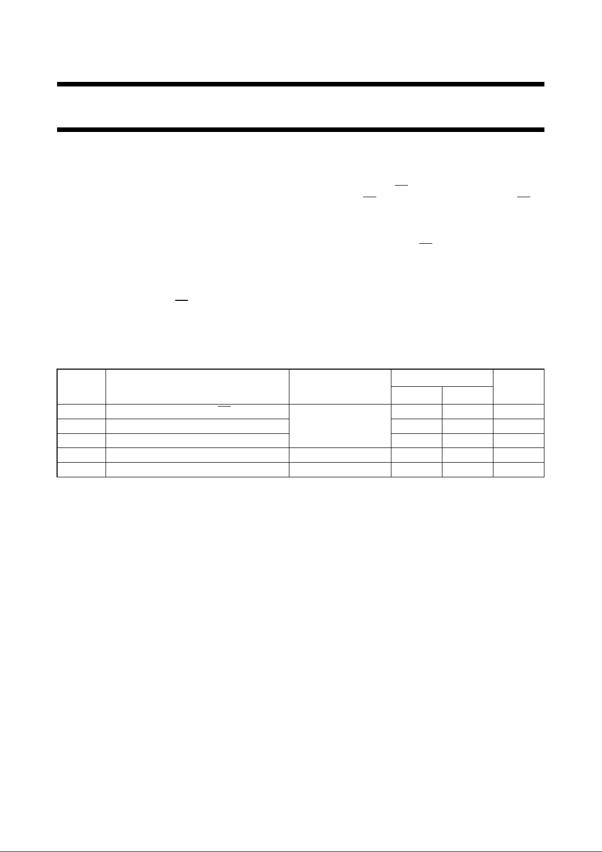
QUICK REFERENCE DATA
GND = 0 V; T
amb
=25°C; tr=tf= 6 ns
Notes
1. C
PD
is used to determine the dynamic power dissipation (PD in µW):
PD=CPD× V
CC
2
× fi+∑(CL× V
CC
2
× fo) where:
fi= input frequency in MHz
fo= output frequency in MHz
∑ (CL× V
CC
2
× fo) = sum of outputs
CL= output load capacitance in pF
VCC= supply voltage in V
2. For HC the condition is VI= GND to V
CC
For HCT the condition is VI= GND to VCC− 1.5 V
ORDERING INFORMATION
See
“74HC/HCT/HCU/HCMOS Logic Package Information”
.
SYMBOL PARAMETER CONDITIONS
TYPICAL
UNIT
HC HCT
t
PHL
/ t
PLH
propagation delay nCP0, nCP1to nQ
n
CL= 15 pF; VCC=5 V 20 24 ns
t
PHL
propagation delay nMR to nQ
n
13 14 ns
f
max
maximum clock frequency 61 55 MHz
C
I
input capacitance 3.5 3.5 pF
C
PD
power dissipation capacitance per counter notes 1 and 2 29 27 pF
Page 3
December 1990 3
Philips Semiconductors Product specification
Dual synchronous BCD counter 74HC/HCT4518
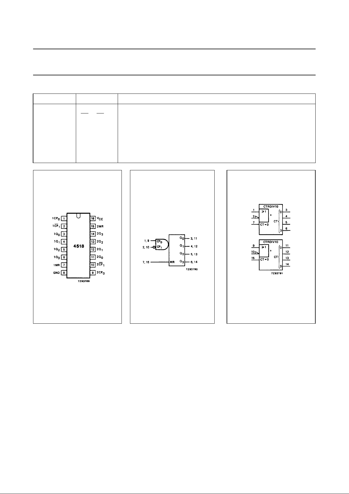
PIN DESCRIPTION
PIN NO. SYMBOL NAME AND FUNCTION
1, 9 1CP
0
, 2CP
0
clock inputs (LOW-to-HIGH, edge-triggered)
2, 10 1
CP1, 2CP
1
clock inputs (HIGH-to-LOW, edge-triggered)
3, 4, 5, 6 1Q
0
to 1Q
3
data outputs
7, 15 1MR, 2MR asynchronous master reset inputs (active HIGH)
8 GND ground (0 V)
11, 12, 13, 14 2Q
0
to 2Q
3
data outputs
16 V
CC
positive supply voltage
Fig.1 Pin configuration. Fig.2 Logic symbol. Fig.3 IEC logic symbol.
Page 4

December 1990 4
Philips Semiconductors Product specification
Dual synchronous BCD counter 74HC/HCT4518
Fig.4 Functional diagram.
FUNCTION TABLE
Notes
1. H = HIGH voltage level
L = LOW voltage level
X = don’t care
↑ = LOW-to-HIGH clock transition
↓ = HIGH-to-LOW clock transition
nCP
0
nCP
1
MR MODE
↑ H L counter advances
L ↓ L counter advances
↓ X L no change
X ↑ L no change
↑ L L no change
H ↓ L no change
XXHQ
0
to Q3= LOW
Fig.5 Logic diagram (one counter).
Fig.6 Timing diagram.
Page 5

December 1990 5
Philips Semiconductors Product specification
Dual synchronous BCD counter 74HC/HCT4518
DC CHARACTERISTICS FOR 74HC
For the DC characteristics see
“74HC/HCT/HCU/HCMOS Logic Family Specifications”
.
Output capability: standard
ICC category: MSI
AC CHARACTERISTICS FOR 74HC
GND = 0 V; t
r=tf
= 6 ns; CL= 50 pF
SYMBOL PARAMETER
T
amb
(°C)
UNIT
TEST CONDITIONS
74HC
V
CC
(V)
WAVEFORMS+25 −40 to +85 −40 to +125
min. typ. max. min. max. min. max.
t
PHL
/ t
PLH
propagation delay
nCP0, nCP1 to nQ
n
66
24
19
210
42
36
265
53
45
315
63
59
ns 2.0
4.5
6.0
Fig.9
t
PHL
propagation delay
nMR to nQ
n
44
16
13
150
30
26
190
38
33
225
45
38
ns 2.0
4.5
6.0
Fig.8
t
THL
/ t
TLH
output transition time 19
7
6
75
15
13
95
19
16
110
22
19
ns 2.0
4.5
6.0
Fig.9
t
W
clock pulse width
HIGH or LOW
80
16
14
25
9
7
100
20
17
120
24
20
ns 2.0
4.5
6.0
Fig.8
t
W
master reset pulse width
HIGH
120
24
20
39
14
11
150
30
26
180
36
31
ns 2.0
4.5
6.0
Fig.8
t
rem
removal time
nMR to nCP0, nCP
1
0
0
0
−22
−8
−6
0
0
0
0
0
0
ns 2.0
4.5
6.0
Fig.8
t
su
set-up time
nCP1 to nCP0;
nCP0 to nCP
1
80
16
14
22
8
6
100
20
17
120
24
20
ns 2.0
4.5
6.0
Fig.7
f
max
maximum clock pulse
frequency
nCP0, nCP
1
6.0
30
35
18
55
66
4.8
24
28
4.0
20
24
MHz 2.0
4.5
6.0
Fig.8
Page 6

December 1990 6
Philips Semiconductors Product specification
Dual synchronous BCD counter 74HC/HCT4518
DC CHARACTERISTICS FOR 74HCT
For the DC characteristics see
“74HC/HCT/HCU/HCMOS Logic Family Specifications”
.
Output capability: standard
ICC category: MSI
Note to HCT types
The value of additional quiescent supply current (∆I
CC
) for a unit load of 1 is given in the family specifications.
To determine ∆ICC per input, multiply this value by the unit load coefficient shown in the table below.
AC CHARACTERISTICS FOR 74HCT
GND = 0 V; t
r=tf
= 6 ns; CL= 50 pF
INPUT UNIT LOAD COEFFICIENT
nCP0, nCP
1
nMR
0.80
1.50
SYMBOL PARAMETER
T
amb
(°C)
UNIT
TEST CONDITIONS
74HCT
V
CC
(V)
WAVEFORMS+25 −40 to +85 −40 to +125
min. typ. max. min. max. min. max.
t
PHL
/ t
PLH
propagation delay
nCP0, nCP1 to nQ
n
28 53 66 80 ns 4.5 Fig.9
t
PHL
propagation delay
nMR to nQ
n
17 35 44 53 ns 4.5 Fig.8
t
THL
/ t
TLH
output transition time 7 15 19 22 ns 4.5 Fig.9
t
W
clock pulse width
HIGH or LOW
20 11 25 30 ns 4.5 Fig.8
t
W
master reset pulse width
HIGH
20 11 25 30 ns 4.5 Fig.8
t
rem
removal time
nMR to nCP0, nCP
1
0 −11 0 0 ns 4.5 Fig.8
t
su
set-up time
nCP1 to nCP0;
nCP0 to nCP
1
16 5 20 24 ns 4.5 Fig.7
f
max
maximum clock pulse
frequency
nCP0, nCP
1
25 50 20 17 MHz 4.5 Fig.8
Page 7

December 1990 7
Philips Semiconductors Product specification
Dual synchronous BCD counter 74HC/HCT4518
AC WAVEFORMS
PACKAGE OUTLINES
See
“74HC/HCT/HCU/HCMOS Logic Package Outlines”
.
Fig.7 Waveforms showing hold and set-up times for nCP0 to nCP1 and nCP1 to nCP0.
(1) HC : VM= 50%; VI= GND to VCC.
HCT: V
M
= 1.3 V; VI= GND to 3 V.
Fig.8 Waveforms showing the minimum pulse widths for nCP0, nCP1 and nMR inputs; the removal time for nMR
and the propagation delay for nMR to nQn outputs and the maximum clock pulse frequency.
Conditions:
nCP1= HIGH while nCP0 is triggered on a
LOW-to-HIGH transition and nCP
0
= LOW,
while n
CP1 is triggered on a HIGH-to-LOW transition.
(1) HC : VM= 50%; VI= GND to VCC.
HCT: V
M
= 1.3 V; VI= GND to 3 V.
Fig.9 Waveforms showing the propagation delays for nCP0, nCP1 to nQn outputs and the output transition times.
Conditions:
nCP1= HIGH while nCP0 is triggered on a
LOW-to-HIGH transition and nCP
0
= LOW,
while n
CP1 is triggered on a HIGH-to-LOW transition.
(1) HC : VM= 50%; VI= GND to VCC.
HCT: V
M
= 1.3 V; VI= GND to 3 V.
 Loading...