

Page 1
Data sheet acquired from Harris Semiconductor
SCHS204J
February 1998 - Revised December 2003
CD54HC4046A, CD74HC4046A,
CD54HCT4046A, CD74HCT4046A
High-Speed CMOS Logic
Phase-Locked Loop with VCO
[ /Title
(CD74
HC404
6A,
CD74
HCT40
46A)
/Subject
(HighSpeed
CMOS
Features
• Operating Frequency Range
- Up to 18MHz (Typ) at V
- Minimum Center Frequency of 12MHz at V
• Choice of Three Phase Comparators
- EXCLUSIVE-OR
- Edge-Triggered JK Flip-Flop
- Edge-Triggered RS Flip-Flop
• Excellent VCO Frequency Linearity
• VCO-Inhibit Control for ON/OFF Keying and for Low
Standby Power Consumption
• Minimal Frequency Drift
• Operating Power Supply Voltage Range
- VCO Section . . . . . . . . . . . . . . . . . . . . . . . . . . 3V to 6V
- Digital Section . . . . . . . . . . . . . . . . . . . . . . . . 2V to 6V
• Fanout (Over Temperature Range)
- Standard Outputs. . . . . . . . . . . . . . . 10 LSTTL Loads
- Bus Driver Outputs . . . . . . . . . . . . . 15 LSTTL Loads
• Wide Operating Temperature Range . . . -55
• Balanced Propagation Delay and Transition Times
• Significant Power Reduction Compared to LSTTL
Logic ICs
• HC Types
- 2V to 6V Operation
- High Noise Immunity: N
at VCC = 5V
• HCT Types
- 4.5V to 5.5V Operation
- Direct LSTTL Input Logic Compatibility,
V
= 0.8V (Max), VIH = 2V (Min)
IL
- CMOS Input Compatibility, I
= 5V
CC
o
= 30%, NIH = 30% of V
IL
≤ 1µA at VOL, VOH
l
= 4.5V
CC
C to 125oC
Applications
Description
The ’HC4046A and ’HCT4046A are high-speed silicon-gate
CMOS devices that are pin compatible with the CD4046B of
the “4000B” series. They are specified in compliance with
JEDEC standard number 7.
The ’HC4046A and ’HCT4046A are phase-locked-loop
circuits that contain a linear voltage-controlled oscillator
(VCO) and three different phase comparators (PC1, PC2 and
PC3). A signal input and a comparator input are common to
each comparator.
The signal input can be directly coupled to large voltage
signals, or indirectly coupled (with a series capacitor) to small
voltage signals. A self-bias input circuit keeps small voltage
signals within the linear region of the input amplifiers. With a
passive low-pass filter, the 4046A forms a second-order loop
PLL. The excellent VCO linearity is achiev ed by the use of
linear op-amp techniques.
Ordering Information
TEMP. RANGE
PART NUMBER
CD54HC4046AF3A -55 to 125 16 Ld CERDIP
CD54HCT4046AF3A -55 to 125 16 Ld CERDIP
CD74HC4046AE -55 to 125 16 Ld PDIP
CD74HC4046AM -55 to 125 16 Ld SOIC
CD74HC4046AMT -55 to 125 16 Ld SOIC
CD74HC4046AM96 -55 to 125 16 Ld SOIC
CD74HC4046ANSR -55 to 125 16 Ld SOP
CC
CD74HC4046APWR -55 to 125 16 Ld TSSOP
CD74HC4046APWT -55 to 125 16 Ld TSSOP
CD74HCT4046AE -55 to 125 16 Ld PDIP
CD74HCT4046AM -55 to 125 16 Ld SOIC
CD74HCT4046AMT -55 to 125 16 Ld SOIC
CD74HCT4046AM96 -55 to 125 16 Ld SOIC
NOTE: When ordering, use the entire part number. The suffixes 96
and R denote tape and reel. The suffix T denotes a small-quantity
reel of 250.
(oC) PACKAGE
• FM Modulation and Demodulation
• Frequency Synthesis and Multiplication
• Frequency Discrimination
• Tone Decoding
• Data Synchronization and Conditioning
• Voltage-to-Frequency Conversion
• Motor-Speed Control
CAUTION: These devices are sensitive to electrostatic discharge. Users should follow proper IC Handling Procedures.
Copyright
© 2003, Texas Instruments Incorporated
1
Page 2
CD54HC4046A, CD74HC4046A, CD54HCT4046A, CD74HCT4046ACD54HC4046A, CD74HC4046A, CD54HCT4046A, CD74HCT4046A
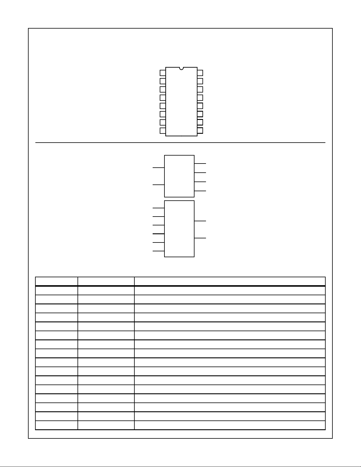
Pinout
Functional Diagram
CD54HC4046A, CD54HCT4046A (CERDIP)
CD74HC4046A (PDIP, SOIC, SOP, TSSOP)
CD74HCT4046A (PDIP, SOIC)
TOP VIEW
16
PCP
PC1
COMP
VCO
COMP
SIG
GND
IN
IN
OUT
OUT
OUT
INH
C1
C1
1
2
3
IN
4
5
6
A
7
B
8
3
14
φ
V
CC
15
PC3
OUT
14
SIG
IN
13
PC2
OUT
12
R
2
11
R
1
10
DEM
OUT
9
VCO
IN
2
PC1
PC3
PC2
PCP
OUT
OUT
OUT
OUT
15
13
1
6
C1
A
C1
VCO
R
R
INH
7
B
11
1
12
2
IN
VCO
9
5
4
VCO
OUT
10
DEM
OUT
Pin Descriptions
PIN NUMBER SYMBOL NAME AND FUNCTION
1 PCP
2 PC1
3 COMP
4 VCO
OUT
OUT
IN
OUT
5 INH Inhibit Input
6C1
7C1
A
B
8 GND Ground (0V)
9 VCO
10 DEM
11 R
12 R
13 PC2
14 SIG
15 PC3
16 V
IN
OUT
1
2
OUT
IN
OUT
CC
Phase Comparator Pulse Output
Phase Comparator 1 Output
Comparator Input
VCO Output
Capacitor C1 Connection A
Capacitor C1 Connection B
VCO Input
Demodulator Output
Resistor R1 Connection
Resistor R2 Connection
Phase Comparator 2 Output
Signal Input
Phase Comparator 3 Output
Positive Supply Voltage
2
Page 3
R2
C1
R1
R5
CD54HC4046A, CD74HC4046A, CD54HCT4046A, CD74HCT4046ACD54HC4046A, CD74HC4046A, CD54HCT4046A, CD74HCT4046A
674314
C1
C1
V
REF
R2
12
+
-
R1
11
10
DEM
OUT
-
+
B
A
VCO
-
+
INH
59
VCO
COMP
OUT
VCO
IN
SIG
IN
IN
PC1
OUT
2
PC2
PC3
OUT
PCP
OUT
V
CC
GND
p
n
OUT
15
13
1
R3
C2
S
D
Q
Q
R
D
CC
V
V
CC
D
CP
D
CP
UP
Q
Q
R
D
Q
DOWN
Q
R
D
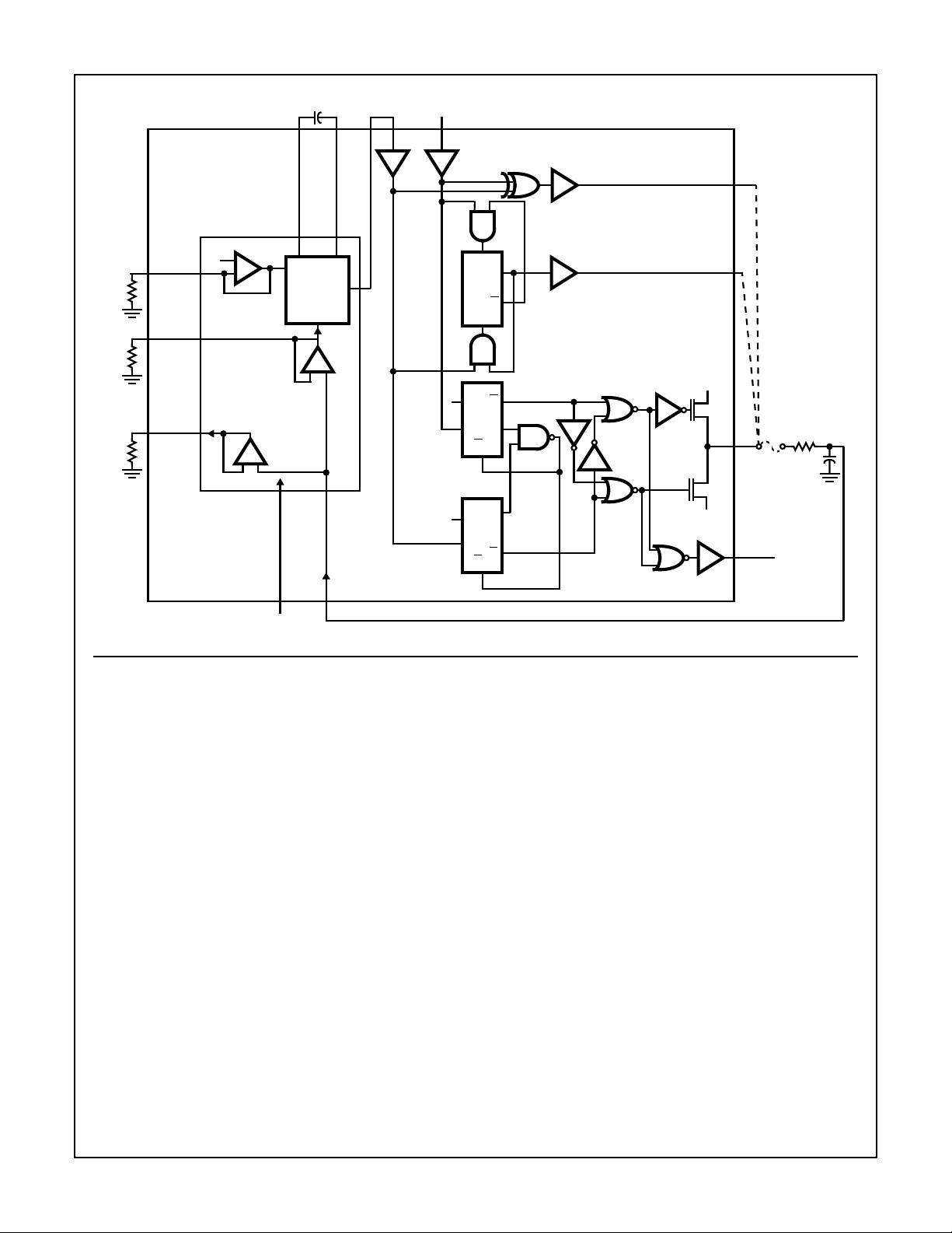
FIGURE 1. LOGIC DIAGRAM
General Description
VCO
The VCO requires one external capacitor C1 (between C1
and C1B) and one external resistor R1 (between R1and
GND) or two external resistors R1 and R2 (between R
GND, and R
determine the frequency range of the VCO. Resistor R2
enables the VCO to have a frequency offset if required. See
logic diagram, Figure 1.
The high input impedance of the VCO simplifies the design
of low-pass filters by giving the designer a wide choice of
resistor/capacitor ranges. In order not to load the low-pass
filter, a demodulator output of the VCO input voltage is
provided at pin 10 (DEM
techniques where the DEM
voltage lower than the VCO input voltage, here the DEM
voltage equals that of the VCO input. If DEM
load resistor (R
GND; if unused, DEM
output (VCO
comparator input (COMP
divider. The VCO output signal has a specified duty factor of
50%. A LOW level at the inhibit input (INH) enables the VCO
and demodulator, while a HIGH level turns both off to
minimize standby power consumption.
and GND). Resistor R1 and capacitor C1
2
). In contrast to conventional
OUT
) should be connected from DEM
S
OUT
) can be connected directly to the
OUT
IN
voltage is one threshold
OUT
is used, a
OUT
OUT
should be left open. The VCO
), or connected via a frequency-
1
and
OUT
Phase Comparators
The signal input (SIG
A
biasing amplifier at pin 14, provided that the signal swing is
) can be directly coupled to the self-
IN
between the standard HC family input logic levels.
Capacitive coupling is required for signals with smaller
swings.
Phase Comparator 1 (PC1)
This is an Exclusive-OR network. The signal and comparator
input frequencies (f
) must have a 50% duty factor to obtain
i
the maximum locking range. The transfer characteristic of
PC1, assuming ripple (f
V
DEMOUT
=(VCC/π)(φSIGIN- φCOMPIN) where V
is the demodulator output at pin 10; V
= 2fi) is suppressed, is:
r
DEMOUT=VPC1OUT
(via low-pass filter).
The average output voltage from PC1, fed to the VCO input
via the low-pass filter and seen at the demodulator output at
to
pin 10 (V
DEMOUT
of signals (SIG
shown in Figure 2. The average of V
V
when there is no signal or noise at SIGIN, and with this
CC
), is the resultant of the phase differences
) and the comparator input (COMPIN)as
IN
is equal to 1/2
DEM
input the VCO oscillates at the center frequency (f
Typical waveforms for the PC1 loop locked at f
o
in Figure 3.
DEMOUT
o
are shown
).
3
Page 4
CD54HC4046A, CD74HC4046A, CD54HCT4046A, CD74HCT4046ACD54HC4046A, CD74HC4046A, CD54HCT4046A, CD74HCT4046A
The frequency capture range (2f
) is defined as the
C
frequency range of input signals on which the PLL will lock if
it was initially out-of-lock. The frequency lock range (2f
L
)is
defined as the frequency range of input signals on which the
loop will stay locked if it was initially in lock. The capture
range is smaller or equal to the lock range.
With PC1, the capture range depends on the low-pass filter
characteristics and can be made as large as the lock range.
This configuration retains lock behavior even with very noisy
input signals. Typical of this type of phase comparator is that
it can lock to input frequencies close to the harmonics of the
VCO center frequency.
V
CC
V
DEMOUT (AV)
1/2 V
CC
0
o
0
o
φ
90
DEMOUT
180
o
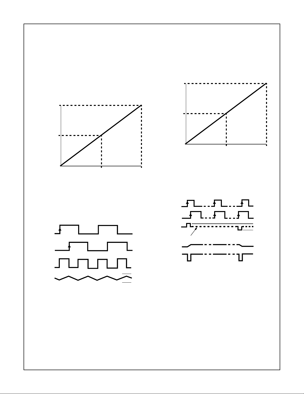
FIGURE 2. PHASE COMPARATOR1: AVERAGE OUTPUT
VOLTAGE vs INPUT PHASE DIFFERENCE:
SIG
COMP
VCO
PC1
VCO
IN
IN
OUT
OUT
IN
V
DEMOUT
φCOMPIN); φ
= V
DEMOUT
= (VCC/π) (φSIGIN -
PC1OUT
=(φSIGIN - φCOMPIN)
V
CC
GND
FIGURE 3. TYPICAL WAVEFORMSFOR PLL USING PHASE
COMPARATOR 1, LOOP LOCKED AT f
o
Phase Comparator 2 (PC2)
This is a positive edge-triggered phase and frequency
detector. When the PLL is using this comparator, the loop
is controlled by positive signal transitions and the duty
factors of SIG
and COMPINare not important. PC2
IN
comprises two D-type flip-flops, control-gating and a threestate output stage. The circuit functions as an up-down
counter (Figure 1) where SIG
COMP
assuming ripple (f
a down-count. The transfer function of PC2,
IN
= fi) is suppressed, is:
r
causes an up-count and
IN
V
DEMOUT
V
DEMOUT
V
DEMOUT
=(VCC/4π)(φSIGIN- φCOMPIN) where
is the demodulator output at pin 10;
=V
PC2OUT
(via low-pass filter).
The average output voltage from PC2, fed to the VCO via the
low-pass filter and seen at the demodulator output at pin 10
(V
DEMOUT
SIG
for the PC2 loop locked at f
V
DEMOUT (AV)
FIGURE 4. PHASE COMPARATOR 2: AVERAGE OUTPUT
FIGURE 5. TYPICAL WAVEFORMS FOR PLL USING PHASE
When the frequencies of SIG
the phase of SIG
driver at PC2
the phase difference (φ
), is the resultant of the phase differences of
and COMPINas shown in Figure 4. Typical waveforms
IN
COMP
VCO
PC2
PCP
V
CC
1/2 V
CC
0
o
-360
VOLTAGE vs INPUT PHASE DIFFERENCE:
V
DEMOUT
= (VCC/4π) (φSIGIN - φCOMPIN);
φ
DEMOUT
SIG
IN
IN
OUT
OUT
HIGH IMPEDANCE OFF - STATE
VCO
IN
OUT
COMPARATOR 2, LOOP LOCKED AT f
leads that of COMPIN, the p-type output
IN
is held “ON” for a time corresponding to
OUT
are shown in Figure 5.
o
o
0
= V
PC2OUT
=(φSIGIN - φCOMPIN)
and COMPINare equal but
IN
DEMOUT
). When the phase of SIG
φ
DEMOUT
V
CC
GND
o
360
o
IN
lags that of COMPIN, the n-type driver is held “ON”.
When the frequency of SIGINis higher than that of
COMP
, the p-type output driver is held “ON” for most of
IN
the input signal cycle time, and for the remainder of the
cycle both n- and p-type drivers are “OFF” (three-state). If
the SIG
frequency is lower than the COMPINfrequency,
IN
then it is the n-type driver that is held “ON” for most of the
cycle. Subsequently, the voltage at the capacitor (C2) of
the low-pass filter connected to PC2
varies until the
OUT
signal and comparator inputs are equal in both phase and
4
Page 5
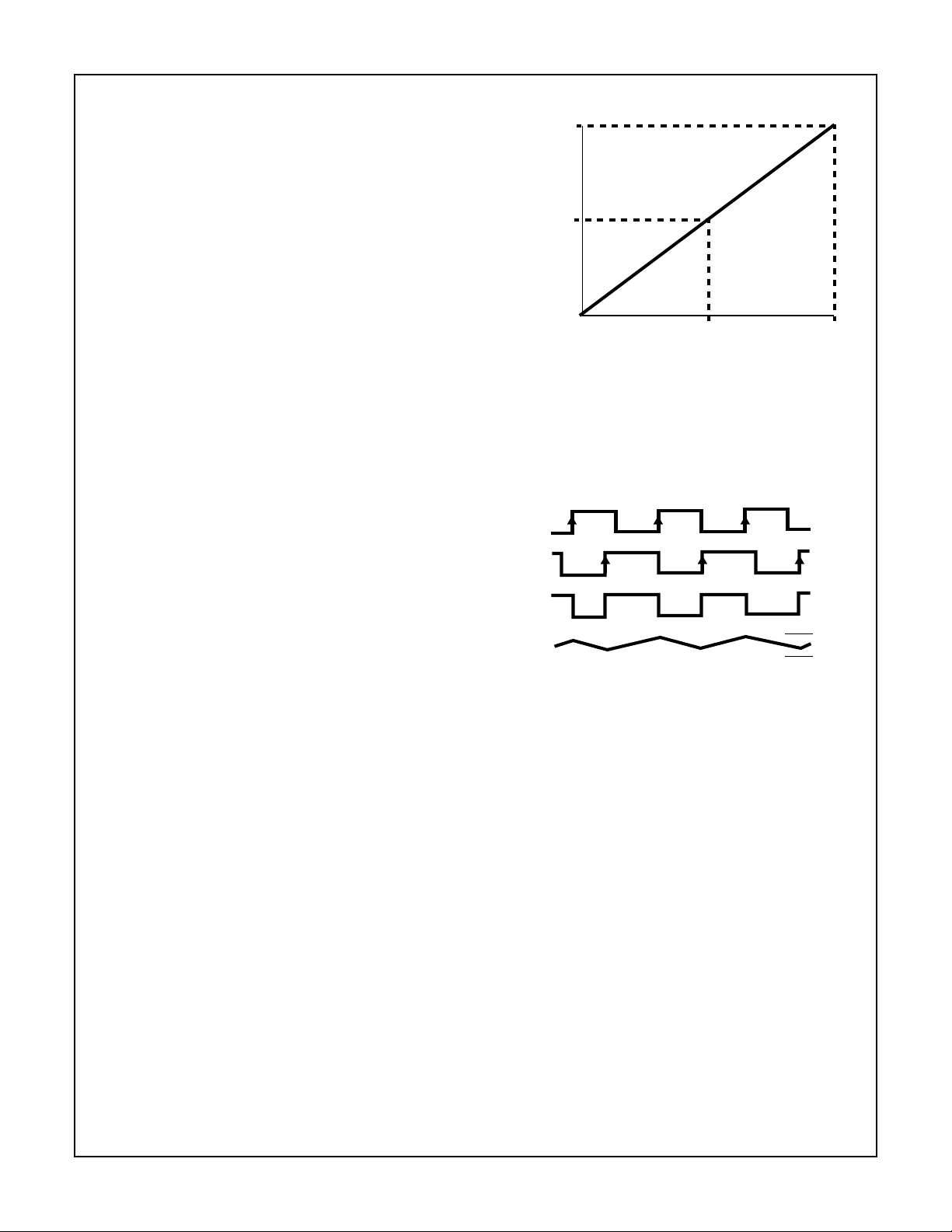
COMPARATOR 3, LOOP LOCKED AT f
CD54HC4046A, CD74HC4046A, CD54HCT4046A, CD74HCT4046A
frequency. At this stable point the voltage on C2 remains
constant as the PC2 output is in three-state and the VCO
input at pin 9 is a high impedance. Also in this condition,
the signal at the phase comparator pulse output (PCP
is a HIGH level and so can be used for indicating a locked
condition.
OUT
)
V
DEMOUT (AV)
V
CC
Thus, for PC2, no phase difference exists between SIG
IN
and COMPINover the full frequency range of the VCO.
Moreover, the power dissipation due to the low-pass filter is
reduced because both p- and n-type drivers are “OFF” for
most of the signal input cycle. It should be noted that the
PLL lock range for this type of phase comparator is equal to
the capture range and is independent of the low-pass filter.
With no signal present at SIG
, the VCO adjusts, via PC2,
IN
to its lowest frequency.
Phase Comparator 3 (PC3)
This is a positive edge-triggered sequential phase
detector using an RS-type flip-flop. When the PLL is using
this comparator, the loop is controlled by positive signal
transitions and the duty factors of SIG
and COMPINare
IN
not important. The transfer character istic of PC3,
assuming ripple (f
V
DEMOUT
V
DEMOUT
= V
PC3OUT
is the demodulator output at pin 10; V
= fi) is suppressed, is:
r
=(VCC/2p) (fSIGIN- fCOMPIN) where
(via low-pass filter).
DEMOUT
The average output from PC3, fed to the VCO via the lowpass filter and seen at the demodulator at pin 10
(V
DEMOUT
SIG
waveforms for the PC3 loop locked at f
), is the resultant of the phase differences of
and COMPINas shown in Figure 6. Typical
IN
are shown in
o
Figure 7.
The phase-to-output response characteristic of PC3
(Figure 6) differs from that of PC2 in that the phase angle
between SIG
and COMPINvaries between 0oand 360
IN
and is 180oat the center frequency. Also PC3 gives a
greater voltage swing than PC2 for input phase differences
but as aconsequence the ripple content of the VCO input
signal is higher. With no signal present at SIG
, the VCO
IN
adjusts, via PC3, to its highest frequency.
1/2 V
CC
0
o
0
FIGURE 6. PHASE COMPARATOR3: AVERAGE OUTPUT
VOLTAGE vs INPUT PHASE DIFFERENCE:
V
DEMOUT
= (VCC/2π) (φSIGIN - φCOMPIN);
φ
DEMOUT
SIG
IN
COMP
IN
VCO
OUT
PC3
OUT
VCO
IN
FIGURE 7. TYPICAL WAVEFORMSFOR PLL USING PHASE
o
= V
PC3OUT
= (φSIGIN - φCOMPIN)
180
o
φ
DEMOUT
360
V
CC
GND
o
The only difference between the HC and HCT versions is the
input level specification of the INH input. This input disables
the VCO section. The comparator’s sections are identical, so
that there is no difference in the SIG
(pin 14) or COMP
IN
(pin 3) inputs between the HC and the HCT versions.
IN
5
Page 6
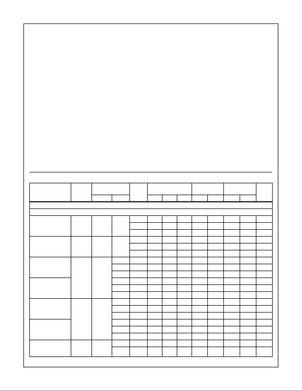
CD54HC4046A, CD74HC4046A, CD54HCT4046A, CD74HCT4046ACD54HC4046A, CD74HC4046A, CD54HCT4046A, CD74HCT4046A
Absolute Maximum Ratings Thermal Information
DC Supply Voltage, VCC. . . . . . . . . . . . . . . . . . . . . . . . -0.5V to 7V
DC Input Diode Current, I
IK
For VI < -0.5V or VI > VCC + 0.5V. . . . . . . . . . . . . . . . . . . . . .±20mA
DC Output Diode Current, I
OK
For VO < -0.5V or VO > VCC + 0.5V . . . . . . . . . . . . . . . . . . . .±20mA
DC Drain Current, per Output, I
O
For -0.5V < VO < VCC + 0.5V. . . . . . . . . . . . . . . . . . . . . . . . . .±25mA
DC Output Source or Sink Current per Output Pin, I
O
For VO > -0.5V or VO < VCC + 0.5V . . . . . . . . . . . . . . . . . . . .±25mA
DC VCC or Ground Current, ICC . . . . . . . . . . . . . . . . . . . . . . . . .±50mA
Operating Conditions
Temperature Range, TA . . . . . . . . . . . . . . . . . . . . . . -55oC to 125oC
Supply Voltage Range, V
HC Types . . . . . . . . . . . . . . . . . . . . . . . . . . . . . . . . . . . . .2V to 6V
HCT Types . . . . . . . . . . . . . . . . . . . . . . . . . . . . . . . . .4.5V to 5.5V
DC Input or Output Voltage, VI, VO . . . . . . . . . . . . . . . . . 0V to V
Input Rise and Fall Time
2V . . . . . . . . . . . . . . . . . . . . . . . . . . . . . . . . . . . . . . 1000ns (Max)
4.5V. . . . . . . . . . . . . . . . . . . . . . . . . . . . . . . . . . . . . . 500ns (Max)
6V . . . . . . . . . . . . . . . . . . . . . . . . . . . . . . . . . . . . . . . 400ns (Max)
CAUTION: Stresses above those listed in “Absolute Maximum Ratings” may cause permanent damage to the device. This is a stress only rating and operation
of the device at these or any other conditions above those indicated in the operational sections of this specification is not implied.
NOTE:
1. The package thermal impedance is calculated in accordance with JESD 51-7.
CC
Package Thermal Impedance, θJA(see Note 1):
E (PDIP) Package . . . . . . . . . . . . . . . . . . . . . . . . . . . . . . .67oC/W
M (SOIC) Package. . . . . . . . . . . . . . . . . . . . . . . . . . . . . . .73oC/W
NS (SOP) Package . . . . . . . . . . . . . . . . . . . . . . . . . . . . . 64oC/W
PW (TSSOP) Package. . . . . . . . . . . . . . . . . . . . . . . . . . 108oC/W
Maximum Junction Temperature. . . . . . . . . . . . . . . . . . . . . . .150oC
Maximum Storage Temperature Range . . . . . . . . . .-65oC to 150oC
Maximum Lead Temperature (Soldering 10s). . . . . . . . . . . . .300oC
(SOIC - Lead Tips Only)
CC
DC Electrical Specifications
PARAMETER SYMBOL
HC TYPES
VCO SECTION
INH High Level Input
Voltage
INH Low Level Input
Voltage
VCO
High Level
OUT
Output Voltage
CMOS Loads
VCO
High Level
OUT
Output Voltage
TTL Loads
VCO
OUT
Low Level
Output Voltage
CMOS Loads
VCO
OUT
Low Level
Output Voltage
TTL Loads
C1A, C1B Low Level
Output Voltage
(Test Purposes Only)
V
IH
V
IL
V
OH
V
OL
V
OL
TEST
CONDITIONS
V
CC
(V)
25oC -40oC TO 85oC -55oC TO 125oC
UNITSVI(V) IO(mA) MIN TYP MAX MIN MAX MIN MAX
- - 3 2.1 - - 2.1 - 2.1 - V
4.5 3.15 - - 3.15 - 3.15 - V
6 4.2 - - 4.2 - 4.2 - V
- - 3 - - 0.9 - 0.9 - 0.9 V
4.5 - - 1.35 - 1.35 - 1.35 V
6 - - 1.8 - 1.8 - 1.8 V
VIHor VIL-0.02 3 2.9 - - 2.9 - 2.9 - V
-0.02 4.5 4.4 - - 4.4 - 4.4 - V
-0.02 6 5.9 - - 5.9 - 5.9 - V
- - ---- - - - V
-4 4.5 3.98 - - 3.84 - 3.7 - V
-5.2 6 5.48 - - 5.34 - 5.2 - V
VIHor VIL0.02 2 - - 0.1 - 0.1 - 0.1 V
0.02 4.5 - - 0.1 - 0.1 - 0.1 V
0.02 6 - - 0.1 - 0.1 - 0.1 V
- - ---- - - - V
4 4.5 - - 0.26 - 0.33 - 0.4 V
5.2 6 - - 0.26 - 0.33 - 0.4 V
VILor V
4 4.5 - - 0.40 - 0.47 - 0.54 V
IH
5.2 6 - - 0.40 - 0.47 - 0.54 V
6
Page 7
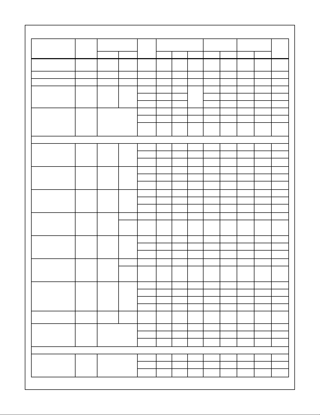
CD54HC4046A, CD74HC4046A, CD54HCT4046A, CD74HCT4046A
DC Electrical Specifications (Continued)
TEST
PARAMETER SYMBOL
INH VCOIN Input
Leakage Current
CONDITIONS
I
VCC or
I
-6--±0.1 - ±1-±1 µA
GND
V
CC
(V)
R1 Range (Note 2) - - - 4.5 3 - 300 - - - - kΩ
R2 Range (Note 2) - - - 4.5 3 - 300 - - - - kΩ
C1 Capacitance
Range
---3--No
4.5 - - - - - - pF
6-- ----pF
VCOIN Operating
Voltage Range
- Over the range
specified for R1 for
LinearitySeeFigure
10, and 34 - 37
3 1.1 - 1.9 - - - - V
4.5 1.1 - 3.2 - - - - V
6 1.1 - 4.6 - - - - V
(Note 3)
PHASE COMPARATOR SECTION
SIGIN, COMP
IN
DC Coupled
High-Level Input
Voltage
SIGIN, COMP
IN
DC Coupled
Low-Level Input
Voltage
PCP
, PCn OUT
OUT
High-Level Output
Voltage
CMOS Loads
PCP
, PCn OUT
OUT
High-Level Output
Voltage
V
IH
- - 2 1.5 - - 1.5 - 1.5 - V
4.5 3.15 - - 3.15 - 3.15 - V
6 4.2 - - 4.2 - 4.2 - V
V
IL
- - 2 - - 0.5 - 0.5 - 0.5 V
4.5 - - 1.35 - 1.35 - 1.35 V
6 - - 1.8 - 1.8 - 1.8 V
V
VILor VIH-0.02 2 1.9 - - 1.9 - 1.9 - V
OH
4.5 4.4 - - 4.4 - 4.4 - V
6 5.9 - - 5.9 - 5.9 - V
V
OH
VILor V
-4 4.5 3.98 - - 3.84 - 3.7 - V
IH
-5.2 6 5.48 - - 5.34 - 5.2 - V
TTL Loads
PCP
Low-Level Output
Voltage
CMOS Loads
PCP
Low-Level Output
Voltage
, PCn OUT
OUT
, PCn OUT
OUT
V
OL
VILor V
0.02 2 - - 0.1 - 0.1 - 0.1 V
IH
4.5 - - 0.1 - 0.1 - 0.1 V
6 - - 0.1 - 0.1 - 0.1 V
V
OL
VILor V
4 4.5 - - 0.26 - 0.33 - 0.4 V
IH
5.2 6 - - 0.26 - 0.33 - 0.4 V
TTL Loads
SIGIN, COMPINInput
Leakage Current
I
VCC or
I
GND
-2--±3-±4-±5 µA
3--±7- ±9-±11 µA
4.5 - - ±18 - ±23 - ±29 µA
6--±30 - ±38 - ±45 µA
PC2
Three-State
OUT
I
OZ
VILor V
-6--±0.5 - ±5-±10 µA
IH
Off-State Current
SIGIN, COMPINInput
Resistance
R
I
VI at Self-Bias
Operation Point:
∆VI = 0.5V,
See Figure 10
3 - 800 - - - - - kΩ
4.5 - 250 - - - - - kΩ
6 - 150 - - - - - kΩ
DEMODULATOR SECTION
Resistor Range R
S
at RS > 300kΩ
Leakage Current
Can Influence
V
DEMOUT
3 50 - 300 - - - - kΩ
4.5 50 - 300 - - - - kΩ
6 50 - 300 - - - - kΩ
25oC -40oC TO 85oC -55oC TO 125oC
UNITSVI(V) IO(mA) MIN TYP MAX MIN MAX MIN MAX
----pF
Limit
7
Page 8
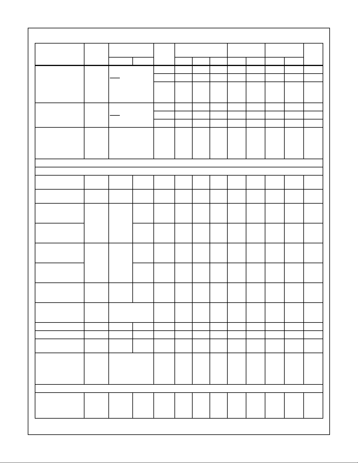
V
C
2
V
C
2
CD54HC4046A, CD74HC4046A, CD54HCT4046A, CD74HCT4046A
DC Electrical Specifications (Continued)
TEST
PARAMETER SYMBOL
OffsetVoltage VCO
to V
DEM
IN
V
OFF
CONDITIONS
VI = V
VCO IN
C
Values Taken Over
V
CC
(V)
=
3-±30 - - - - - mV
4.5 - ±20 - - - - - mV
6-±10 - - - - - mV
RS Range
See Figure 23
Dynamic Output
Resistance at
DEM
OUT
Quiescent Device
Current
R
D
V
C
DEMOUT
=3-25-----Ω
4.5 - 25 - - - - - Ω
6 - 25 - - - - - Ω
I
CC
Pins 3, 5 and 14
6 - - 8 - 80 - 160 µA
at VCC Pin 9 at
GND, I1 at Pins 3
and 14 to be
excluded
HCT TYPES
VCO SECTION
INH High Level Input
Voltage
INH Low Level Input
Voltage
VCO
High Level
OUT
V
IH
- - 4.5 to
5.5
V
IL
- - 4.5 to
5.5
V
VIHor VIL-0.02 4.5 4.4 - - 4.4 - 4.4 - V
OH
Output Voltage
CMOS Loads
VCO
High Level
OUT
-4 4.5 3.98 - - 3.84 - 3.7 - V
Output Voltage
TTL Loads
VCO
OUT
Low Level
V
VIHor VIL0.02 4.5 - - 0.1 - 0.1 - 0.1 V
OL
Output Voltage
CMOS Loads
VCO
OUT
Low Level
4 4.5 - - 0.26 - 0.33 - 0.4 V
Output Voltage
TTL Loads
C1A, C1B Low Level
V
OL
VIHor V
4 4.5 - - 0.40 - 0.47 - 0.54 V
IL
Output Voltage
(Test Purposes Only)
INH VCOIN Input
Leakage Current
I
I
Any Voltage
Between VCC and
5.5 - ±0.1 - ±1-±1 µA
GND
R1 Range (Note 2) - - - 4.5 3 - 300 - - - - kΩ
R2 Range (Note 2) - - - 4.5 3 - 300 - - - - kΩ
C1 Capacitance
- - - 4.5 0 - No
Range
VCOIN Operating
Voltage Range
- Over the range
specified for R1 for
4.5 1.1 - 3.2 - - - - V
LinearitySeeFigure
10, and 34 - 37
(Note 3)
PHASE COMPARATOR SECTION
SIGIN, COMP
DC Coupled
IN
V
IH
- - 4.5 to
5.5
High-Level Input
Voltage
25oC -40oC TO 85oC -55oC TO 125oC
UNITSVI(V) IO(mA) MIN TYP MAX MIN MAX MIN MAX
2--2- 2 - V
- - 0.8 - 0.8 - 0.8 V
----pF
Limit
2--2- 2 - V
8
Page 9
V
C
2
V
C
2
CD54HC4046A, CD74HC4046A, CD54HCT4046A, CD74HCT4046A
DC Electrical Specifications (Continued)
TEST
CONDITIONS
PARAMETER SYMBOL
SIGIN, COMP
IN
DC Coupled
Low-Level Input
Voltage
PCP
, PCn OUT
OUT
High-Level Output
Voltage
CMOS Loads
PCP
, PCn OUT
OUT
High-Level Output
Voltage
TTL Loads
PCP
, PCn OUT
OUT
Low-Level Output
Voltage
CMOS Loads
PCP
, PCn OUT
OUT
Low-Level Output
Voltage
TTL Loads
SIGIN, COMPINInput
Leakage Current
PC2
Three-State
OUT
Off-State Current
SIGIN, COMPINInput
Resistance
DEMODULATOR SECTION
Resistor Range R
OffsetVoltage VCO
to V
DEM
V
IL
V
OH
V
OH
V
OL
V
OL
I
I
- - 4.5 to
VILor V
IH
VILor V
IH
VILor V
IH
VILor V
IH
Any
Voltage
Between
VCCand
GND
I
VILor V
OZ
R
I
IH
VI at Self-Bias
Operation Point:
∆VI = 0.5V,
See Figure 10
S
at RS > 300kΩ
Leakage Current
Can Influence
V
DEM OUT
V
IN
OFF
VI = V
C
VCO IN
V
CC
(V)
25oC -40oC TO 85oC -55oC TO 125oC
UNITSVI(V) IO(mA) MIN TYP MAX MIN MAX MIN MAX
- - 0.8 - 0.8 - 0.8 V
5.5
- 4.5 4.4 - - 4.4 - 4.4 - V
- 4.5 3.98 - - 3.84 - 3.7 - V
- 4.5 - - 0.1 - 0.1 - 0.1 V
- 4.5 - - 0.26 - 0.33 - 0.4 V
- 5.5 - - ±30 ±38 ±45 µA
- 5.5 - - ±0.5 ±5- -±10 µA
4.5 - 250 - - - - - kΩ
4.5 5 - 300 - - - - kΩ
=
4.5 - ±20 - - - - - mV
Values tak en over
RS Range
See Figure 23
Dynamic Output
Resistance at
DEM
OUT
Quiescent Device
Current
Additional Quiescent
Device Current Per
Input Pin: 1 Unit Load
R
D
I
CC
∆I
CC
(Note 4)
V
DEM OUT
C
VCC or
GND
V
CC
-2.1
Excluding
= 4.5 - 25 - - - - - Ω
- 5.5 - - 8 - 80 - 160 µA
- 4.5 to
- 100 360 - 450 - 490 µA
5.5
Pin 5
NOTES:
2. The value for R1 and R2 in parallel should exceed 2.7kΩ.
3. The maximum operating voltage can be as high as VCC -0.9V, however, this may result in an increased offset voltage.
4. For dual-supply systems theoretical worst case (VI = 2.4V, VCC = 5.5V) specification is 1.8mA.
9
Page 10
CD54HC4046A, CD74HC4046A, CD54HCT4046A, CD74HCT4046A
HCT Input Loading Table
INPUT UNIT LOADS
INH 1
NOTE: Unitload is ∆ICClimit specific in DC Electrical Specifications
Table, e.g., 360µA max. at 25oC.
Switching Specifications C
PARAMETER SYMBOL
HC TYPES
PHASE COMPARATOR SECTION
Propagation Delay t
SIGIN, COMPIN to PCI
SIGIN, COMPIN to PCP
SIGIN, COMPIN to PC3
Output Transition Time t
Output Enable Time, SIGIN,
COMPIN to PC2
OUT
Output Disable Time, SIGIN,
COMPIN to PC2
OUT
AC Coupled Input Sensitivity
(
) at SIGIN or COMP
P-P
VCO SECTION
Frequency Stability with
Temperature Change
Maximum Frequency f
OUT
OUT
OUT
IN
= 50pF, Input tr, tf= 6ns
L
TEST
CONDITIONS VCC(V)
, t
PLH
PHL
, t
THL
TLH
t
, t
PZH
PZL
t
, t
PHZ
PLZ
V
I(P-P)
∆f
∆T
MAX
R1 = 100kΩ,
R
= ∞
2
C1 = 50pF
R1 = 3.5kΩ
R
= ∞
2
C1 = 0pF
R1 = 9.1kΩ
R
= ∞
2
25oC
-40oC TO
85oC
-55oC TO
125oC
UNITSMIN TYP MAX MIN MAX MIN MAX
2 - - 200 - 250 - 300 ns
4.5 - - 40 - 50 - 60 ns
6 - - 34 - 43 - 51 ns
2 - - 300 - 375 - 450 ns
4.5 - - 60 - 75 - 90 ns
6 - - 51 - 64 - 77 ns
2 - - 245 - 305 - 307 ns
4.5 - - 49 - 61 - 74 ns
6 - - 42 - 52 - 63 ns
2 - - 75 - 95 - 110 ns
4.5 - - 15 - 19 - 22 ns
6 - - 13 - 16 - 19 ns
2 - - 265 - 330 - 400 ns
4.5 - - 53 - 66 - 80 ns
6 - - 45 - 56 - 68 ns
2 - - 315 - 395 - 475 ns
4.5 - - 63 - 79 - 95 ns
6 - - 54 - 67 - 81 ns
3 - 11 - - - - - mV
4.5 - 15 - - - - - mV
6 - 33 - - - - - mV
3 - 0.11 - - - - - %/oC
4.5 - 0.11 - - - - - %/oC
6 - 0.11 - - - - - %/oC
3 - 24 - - - - - MHz
4.5 - 24 - - - - - MHz
6 - 24 - - - - - MHz
3 - 38 - - - - - MHz
4.5 - 38 - - - - - MHz
6 - 38 - - - - - MHz
10
Page 11
CD54HC4046A, CD74HC4046A, CD54HCT4046A, CD74HCT4046A
Switching Specifications C
= 50pF, Input tr, tf= 6ns (Continued)
L
TEST
PARAMETER SYMBOL
CONDITIONS VCC(V)
Center Frequency C1 = 40pF
R1 = 3kΩ
R
= ∞
2
VCOIN =
VCC/2
Frequency Linearity ∆f
VCO
R1 = 100kΩ
R
= ∞
2
C1 = 100pF
Offset Frequency R2 = 220kΩ
C1 = 1nF
DEMODULATOR SECTION
V
OUT VS fIN
R1 = 100kΩ
R
= ∞
2
C1 = 100pF
RS = 10kΩ
R3 = 100kΩ
C2 = 100pF
HCT TYPES
PHASE COMPARATOR SECTION
Propagation Delay t
SIGIN, COMPIN to PCI
SIGIN, COMPIN to PCP
SIGIN, COMPIN to PC3
Output Transition Time t
Output Enable Time, SIGIN,
COMPIN to PC2
OUT
Output Disable Time, SIGIN,
COMPIN to PCZ
OUT
AC Coupled Input Sensitivity
(
) at SIGIN or COMP
P-P
I
PHL,tPLH
OUT
OUTtPHL,tPLH
OUTtPHL,tPLH
, t
TLH
THL
t
, t
PZH
t
, t
PHZ
CL = 50pF 4.5 - - 45 - 56 - 68 ns
CL = 50pF 4.5 - - 68 - 85 - 102 ns
CL = 50pF 4.5 - - 58 - 73 - 87 ns
CL = 50pF 4.5 - - 15 - 19 - 22 ns
CL = 50pF 4.5 - - 60 - 75 - 90 pF
PZL
CL = 50pF 4.5 - - 68 - 85 - 102 pF
PLZ
V
I(P-P)
VCO SECTION
Frequency Stability with
Temperature Change
Maximum Frequency f
∆f
∆T
MAX
R1 = 100kΩ,
R
= ∞
2
C1 = 50pF
R1 = 3.5kΩ
R
= ∞
2
C1 = 0pF
R1 = 9.1kΩ
R
= ∞
2
Center Frequency C1 = 40pF
R1 = 3kΩ
R
= ∞
2
VCOIN =
VCC/2
Frequency Linearity ∆f
VCO
R1 = 100kΩ
R
= ∞
2
C1 = 100pF
25oC
-40oC TO
85oC
-55oC TO
125oC
UNITSMIN TYP MAX MIN MAX MIN MAX
3 7 10 - - - - - MHz
4.5 12 17 - - - - - MHz
6 14 21 - - - - - MHz
3 - 0.4 - - - - - %
4.5 - 0.4 - - - - - %
6 - 0.4 - - - - - %
3 - 400 - - - - - kHz
4.5 - 400 - - - - - kHz
6 - 400 - - - - - kHz
3 - - - - - - - mV/kHz
4.5 - 330 - - - - - mV/kHz
6 - - - - - - - mV/kHz
4.5 - 15 - - - - - mV
4.5 - 0.11 - - - - - %/oC
4.5 - 24 - - - - - MHz
4.5 - 38 - - - - - MHz
4.5 12 17 - - - - - MHz
4.5 - 0.4 - - - - - %
11
Page 12
CD54HC4046A, CD74HC4046A, CD54HCT4046A, CD74HCT4046A
Switching Specifications C
= 50pF, Input tr, tf= 6ns (Continued)
L
TEST
PARAMETER SYMBOL
CONDITIONS VCC(V)
Offset Frequency R2 = 220kΩ
C1 = 1nF
DEMODULATOR SECTION
V
OUT VS fIN
R1 = 100kΩ
R
= ∞
2
C1 = 100pF
RS = 10kΩ
R3 = 100kΩ
C2 = 100pF
Test Circuits and Waveforms
SIGINCOMP
INPUTS
PCP
PC3
OUT
OUT
IN
PC1
OUT
OUTPUTS
t
TLH
t
V
PHL
S
t
PHL
V
S
25oC
-40oC TO
85oC
-55oC TO
125oC
4.5 - 400 - - - - - kHz
4.5 - 330 - - - - - mV/kHz
SIG
t
TLH
IN
INPUTS
COMP
INPUTS
PC2
OUT
OUTPUT
V
S
IN
t
PZH
V
S
t
PZH
90%
V
S
t
PZL
t
PZL
UNITSMIN TYP MAX MIN MAX MIN MAX
10%
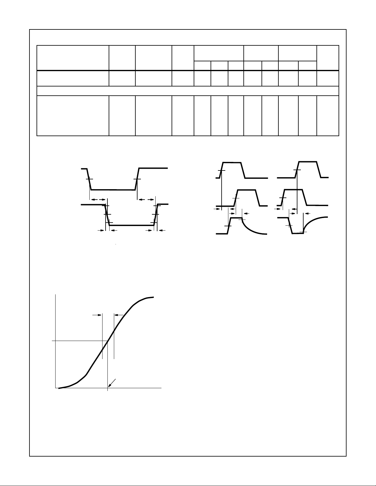
FIGURE 8. INPUT TOOUTPUT PROPAGATION DELAYSAND
OUTPUT TRANSITION TIMES
Typical Performance Curves
I
I
∆V
I
SELF-BIAS OPERATING POINT
V
I
FIGURE 10. TYPICAL INPUT RESISTANCE CURVE AT SIGIN,
COMP
IN
FIGURE 9. THREE STATEENABLE AND DISABLE TIMES FOR
PC2
OUT
12
Page 13
CD54HC4046A, CD74HC4046A, CD54HCT4046A, CD74HCT4046A
Typical Performance Curves (Continued)
8
10
7
10
6
10
5
10
4
10
3
10
2
10
CENTER FREQUENCY (Hz)
VCOIN = 0.5 V
10
VCC= 4.5V
1
110
CC
2
10
3
10
10
4
R1 = 2.2K
R1 = 22K
R1 = 220K
R1 = 2.2M
R1 = 11M
5
10
10
CAPACITANCE, C1 (pF)
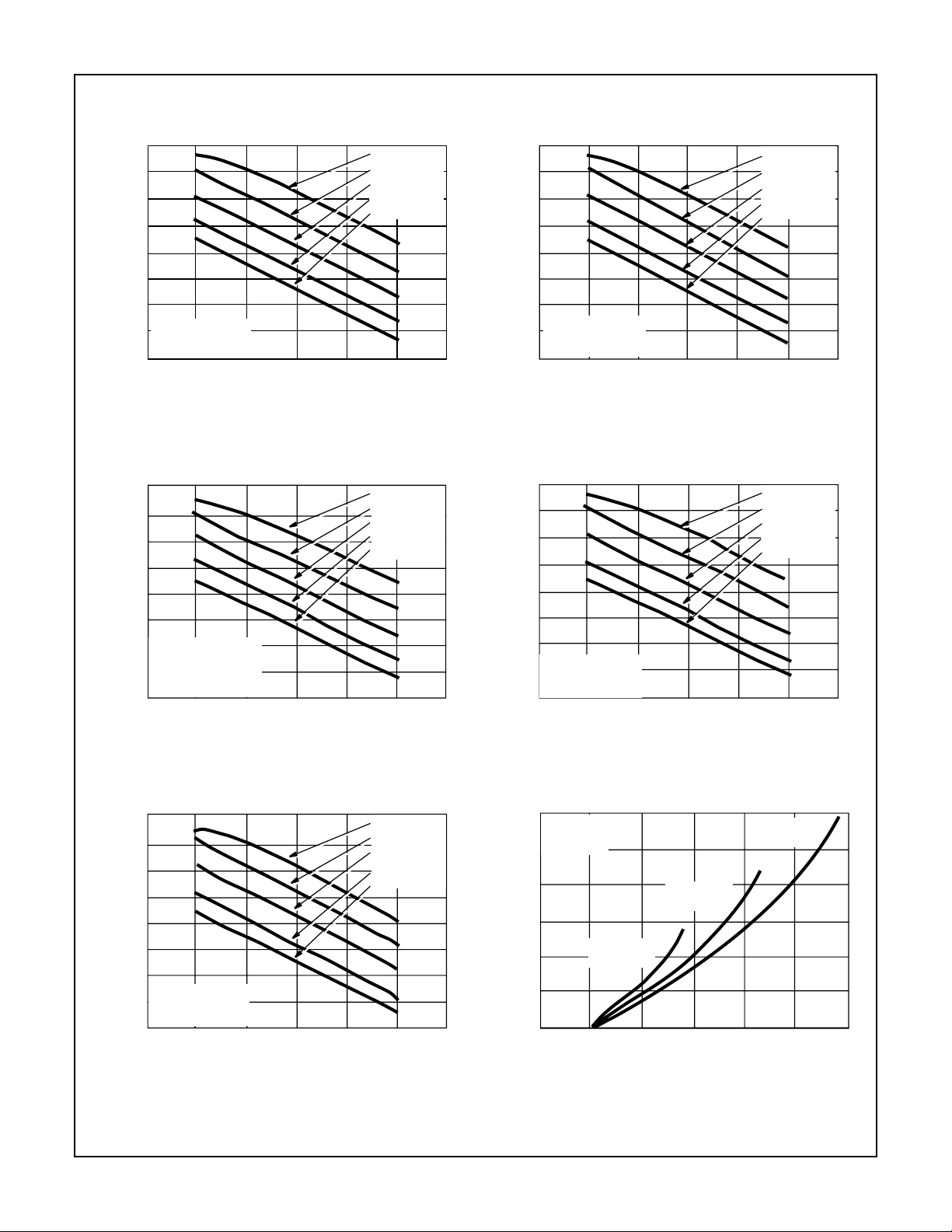
FIGURE 11. HC4046A TYPICAL CENTER FREQUENCY vs R1,
C1 (VCC = 4.5V)
8
10
7
10
6
10
5
10
4
10
3
10
2
10
VCOIN = 0.5 V
CENTER FREQUENCY (Hz)
VCC= 3.0V
10
R2 = OPEN
1
110
CC
2
10
3
10
CAPACITANCE, C1 (pF)
10
4
R1 = 1.5K
R1 = 15K
R1 = 150K
R1 = 1.5M
R1 = 7.5M
5
10
10
8
10
7
10
6
10
5
10
4
10
3
10
2
10
CENTER FREQUENCY (Hz)
VCOIN = 0.5 V
10
CC
VCC= 6.0V
6
1
110
2
10
3
10
4
10
CAPACITANCE, C1 (pF)
FIGURE 12. HC4046A TYPICAL CENTER FREQUENCY vs R1,
C1 (VCC = 6V)
8
10
7
10
6
10
5
10
4
10
3
10
2
10
CENTER FREQUENCY (Hz)
VCOIN = 0.5 V
10
VCC= 4.5V
6
1
110
CC
2
10
3
10
CAPACITANCE, C1 (pF)
4
10
R1 =3K
R1 = 30K
R1 =330K
R1 = 3M
R1 = 15M
5
10
R1 = 2.2K
R1 = 22K
R1 = 220K
R1 = 2.2M
R1 = 11M
5
10
6
10
6
10
FIGURE 13. HC4046A TYPICAL CENTER FREQUENCY vs R1,
C1 (VCC = 3V, R2 = OPEN)
8
10
7
10
6
10
5
10
4
10
3
10
2
10
CENTER FREQUENCY (Hz)
VCOIN = 0.5 V
10
VCC= 5.5V
1
110
CC
2
10
3
10
10
4
R1 = 3K
R1 = 30K
R1 = 300K
R1 = 3M
R1 = 15M
5
10
10
CAPACITANCE, C1 (pF)
FIGURE 15. HCT4046A TYPICAL CENTER FREQUENCY vs R1,
C1 (VCC = 5.5V)
FIGURE 14. HCT4046A TYPICAL CENTER FREQUENCY vs R1,
C1 (VCC = 4.5V)
140
120
C1 = 50pF
R1 = 1.5M
VCC = 6V
100
VCC = 4.5V
80
60
VCO FREQUENCY (kHz)
40
6
20
01 2 3456
VCC = 3V
VCO
(V)
IN
FIGURE 16. HC4046A TYPICAL VCO FREQUENCY vs VCO
(R1 = 1.5MΩ, C1 = 50pF)
13
IN
Page 14
CD54HC4046A, CD74HC4046A, CD54HCT4046A, CD74HCT4046A
Typical Performance Curves (Continued)
90
C1 = 0.1µF
80
R1 = 1.5M
70
60
50
40
30
VCO FREQUENCY (Hz)
20
10
01 23 45 6
VCC = 3V
VCC = 4.5V
VCO
(V)
IN
VCC = 6V
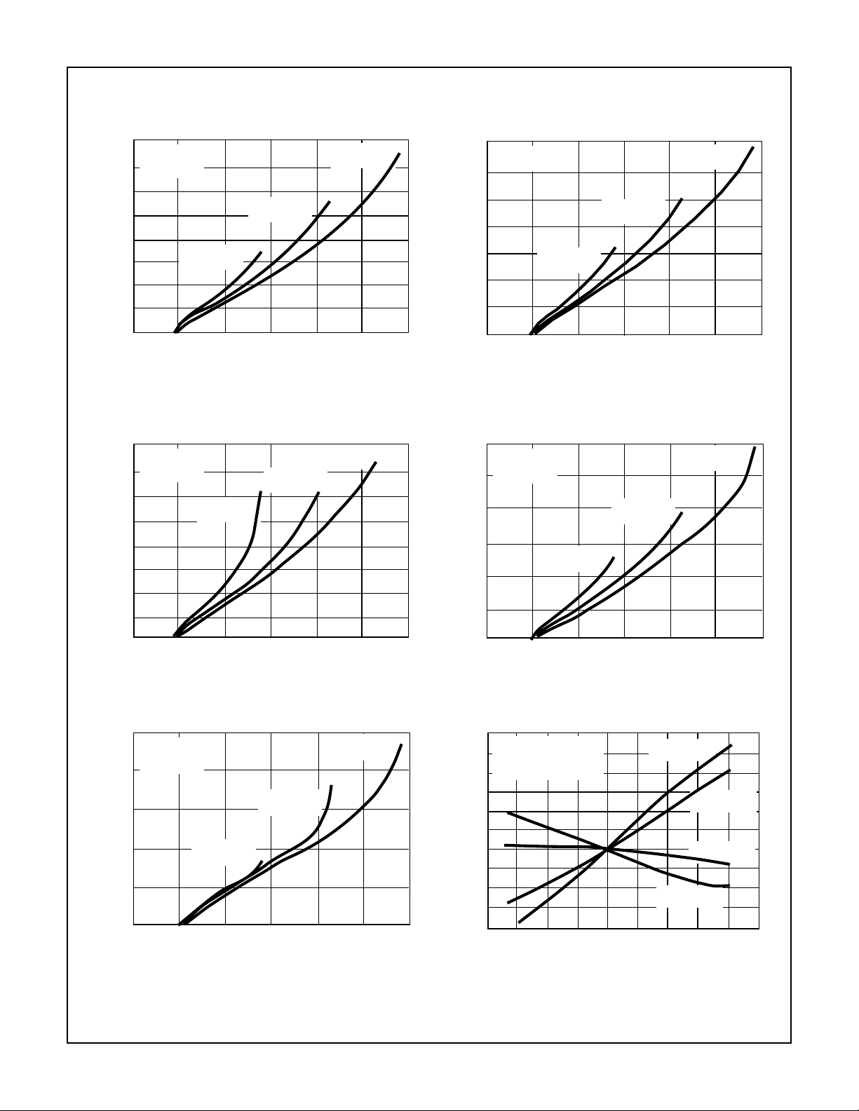
FIGURE 17. HC4046A TYPICAL VCO FREQUENCY vs VCO
(R1 = 1.5MΩ, C1 = 0.1µF)
18
C1 = 0.1µF
16
R1 = 5.6k
14
12
10
8
6
VCO FREQUENCY (kHz)
4
2
01 23 45 6
VCC = 3V
VCO
VCC = 4.5V
(V)
IN
VCC = 6V
FIGURE 19. HC4046A TYPICAL VCO FREQUENCY vs VCO
(R1 = 5.6kΩ, C1 = 0.1µF)
800
C1 = 0.1µF
R1 = 150K
700
600
500
400
300
VCO FREQUENCY (Hz)
200
100
01 23 45 6
IN
FIGURE 18. HC4046A TYPICAL VCO FREQUENCY vs VCO
VCC = 3V
VCC = 4.5V
(V)
VCO
IN
VCC = 6V
IN
(R1 = 150kΩ, C1 = 0.1µF)
1400
C1 = 50pF
R1 = 150K
1200
1000
800
VCC = 3V
600
VCO FREQUENCY (kHz)
400
200
01 23 45 6
IN
FIGURE 20. HC4046A TYPICAL VCO FREQUENCY vs VCO
VCC = 4.5V
VCO
IN
(V)
VCC = 6V
IN
(R1 = 150kΩ, C1 = 50pF)
24
C1 = 50pF
R1 = 5.6K
20
16
12
VCO FREQUENCY (MHz)
8
4
01 23 45 6
VCC = 3V
VCC = 4.5V
VCO
IN
(V)
VCC = 6V
FIGURE 21. HC4046A TYPICAL VCO FREQUENCY vs VCO
(R1 = 5.6kΩ, C1 = 50pF)
24
VCOIN = 0.5 V
20
C1 = 50pF, VCC = 3V
R2 = OPEN
16
12
8
4
0
-4
-8
VCO FREQUENCY CHANGE, ∆f (%)
-12
-16
-75 -50 -25 0 25 50 75
IN
FIGURE 22. HC4046A TYPICAL CHANGE IN VCO FREQUENCY
CC
AMBIENT TEMPERATURE, T
R1 = 1.5M
R1 = 150K
R1 = 3K
R1 = 1.5K
100 125 150
(oC)
A
vs AMBIENT TEMPERATURE AS A FUNCTION OF
R1 (VCC = 3V)
14
Page 15
CD54HC4046A, CD74HC4046A, CD54HCT4046A, CD74HCT4046A
Typical Performance Curves (Continued)
VCOIN = 0.5 V
20
C1 = 50pF, VCC = 4.5V
16
R2 = OPEN
12
8
4
0
-4
-8
VCO FREQUENCY CHANGE, ∆f (%)
-12
-75 -50 -25 0 25 50 75
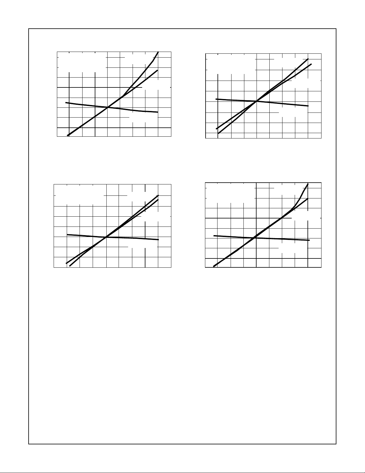
FIGURE 23. HC4046A TYPICAL CHANGE IN VCO FREQUENCY
vs AMBIENT TEMPERATURE AS A FUNCTION OF
R1 (VCC = 4.5V)
CC
AMBIENT TEMPERATURE, TA (oC)
R1 = 2.2M
R1 = 2.2K
100 125 150
R1 = 220K
VCOIN = 0.5 V
16
C1 = 50pF, VCC = 6.0V
12
R2 = OPEN
8
4
0
-4
-8
VCO FREQUENCY CHANGE, ∆f (%)
-12
-75 -50 -25 0 25 50 75
CC
AMBIENT TEMPERATURE, T
R1 = 3M
R1 = 300K
R1 = 3K
100 125 150
(oC)
A
FIGURE 24. HC4046A TYPICAL CHANGE IN VCO FREQUENCY
vs AMBIENT TEMPERATURE AS A FUNCTION OF
R1 (VCC = 6V)
20
VCOIN = 0.5 V
C1 = 50pF, VCC = 5.5V
16
R2 = OPEN
12
8
4
0
-4
-8
VCO FREQUENCY CHANGE, ∆f (%)
-12
-75 -50 -25 0 25 50 75
CC
AMBIENT TEMPERATURE, T
R1 = 3M
R1 = 300K
R1 = 3K
100 125 150
(oC)
A
FIGURE 25. HCT4046A TYPICAL CHANGE IN VCO
FREQUENCY vs AMBIENT TEMPERATURE AS A
FUNCTION OF R1
VCOIN = 0.5 V
20
C1 = 50pF, VCC = 4.5V
16
R2 = OPEN
12
8
4
0
-4
-8
VCO FREQUENCY CHANGE, ∆f (%)
-12
-75 -50 -25 0 25 50 75
CC
AMBIENT TEMPERATURE, T
R1 = 2.2M
R1 = 220K
R1 = 2.2K
100 125 150
(oC)
A
FIGURE 26. HC4046A TYPICAL CHANGE IN VCO FREQUENCY
vs AMBIENT TEMPERATURE AS A FUNCTION OF
R1 (VCC = 4.5V)
15
Page 16
CD54HC4046A, CD74HC4046A, CD54HCT4046A, CD74HCT4046A
Typical Performance Curves (Continued)
8
10
7
10
6
10
5
10
4
10
3
10
2
10
OFFSET FREQUENCY (Hz)
VCOIN = 0.5 V
10
VCC = 4.5V
1
110
CC
2
10
3
10
10
4
R2 = 2.2K
R2 = 22K
R2 = 220K
R2 = 2.2M
R2 = 11M
5
10
CAPACITANCE, C1 (pF)
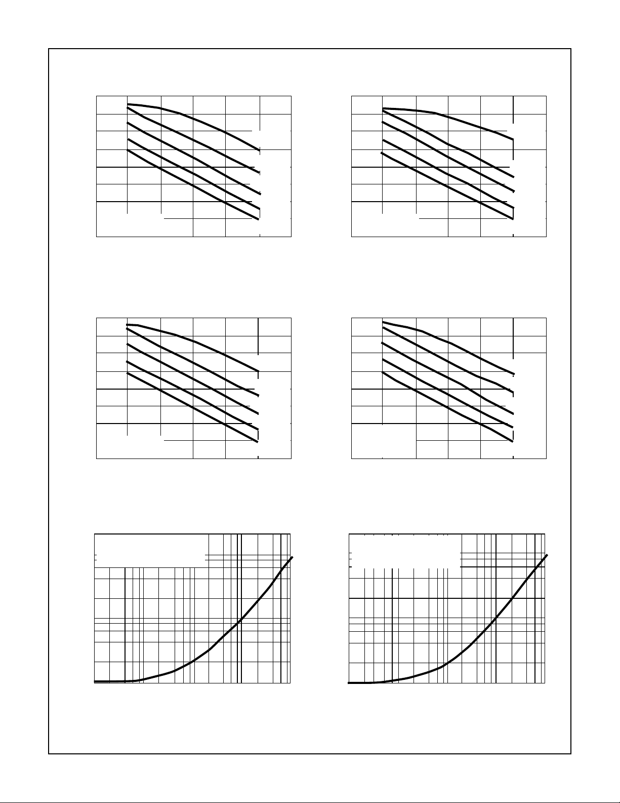
FIGURE 27. HC4046A OFFSET FREQUENCY vs R2, C1
(VCC = 4.5V)
8
10
7
10
6
10
5
10
4
10
3
10
2
10
OFFSET FREQUENCY (Hz)
VCOIN = 0.5 V
10
VCC = 4.5V
1
110
CC
2
10
3
10
CAPACITANCE, C1 (pF)
10
4
R2 = 2.2K
R2 = 22K
R2 = 220K
R2 = 2.2M
R2 = 11M
5
10
8
10
7
10
6
10
5
10
4
10
3
10
2
10
OFFSET FREQUENCY (Hz)
VCOIN = 0.5 V
10
VCC = 3V
6
10
1
110
CC
2
10
3
10
10
4
R2 = 1.5K
R2 = 15K
R2 = 150K
R2 = 1.5M
R2 = 7.5M
5
10
6
10
CAPACITANCE, C1 (pF)
FIGURE 28. HC4046A OFFSET FREQUENCY vs R2, C1
(VCC = 3V)
8
10
7
10
6
10
5
10
4
10
3
10
2
10
OFFSET FREQUENCY (Hz)
VCOIN = 0.5 V
HC VCC = 6V
10
HCT V
6
10
1
110
CC
= 5.5V
CC
2
10
3
10
4
10
CAPACITANCE, C1 (pF)
R2 = 3K
R2 = 30K
R2 = 300K
R2 = 3M
R2 = 15M
5
10
6
10
FIGURE 29. HCT4046A OFFSET FREQUENCY vs R2, C1
(VCC = 4.5V)
PIN 9 = 0.95 VCC FOR f
PIN 9 = 0V FOR f
2
10
VCC = 3V, 4.5V, 6V
MIN
/f
10
MAX
f
0
-2
10
10
FIGURE 31. HC4046A f
-1
MIN
MIN/fMAX
MAX
1
10
R2/R1
vs R2/R1 (VCC = 3V, 4.5V, 6V) FIGURE 32. HCT4046A f
FIGURE 30. HC4046A AND HCT4046A OFFSET FREQUENCY
vs R2, C1 (VCC = 6V, VCC = 5.5V)
PIN 9 = 0.95 VCC FOR f
2
PIN 9 = 0V FOR f
10
VCC = 4.5V TO 5.5V
MIN
/f
10
MAX
f
0
2
10
-2
10
-1
10
MAX
MIN
MAX/fMIN
1
10
R2/R1
vs R2/R1 (VCC= 4.5V TO 5.5V)
2
10
16
Page 17
:
CD54HC4046A, CD74HC4046A, CD54HCT4046A, CD74HCT4046A
Typical Performance Curves (Continued)
8
C1 = 50pF
= 4.5V
V
6
CC
R2 = OPEN
f
f
2
f
0
f
0
f
1
∆V
MIN MAX
1/2V
∆V
CC
∆V = 0.5V OVER THE VCC RANGE
FOR VCO LINEARITY
= f1 + f
f’
o
2
2
f’
- f
o
o
LINEARITY =
V
VCOIN
x 100%
f’
o
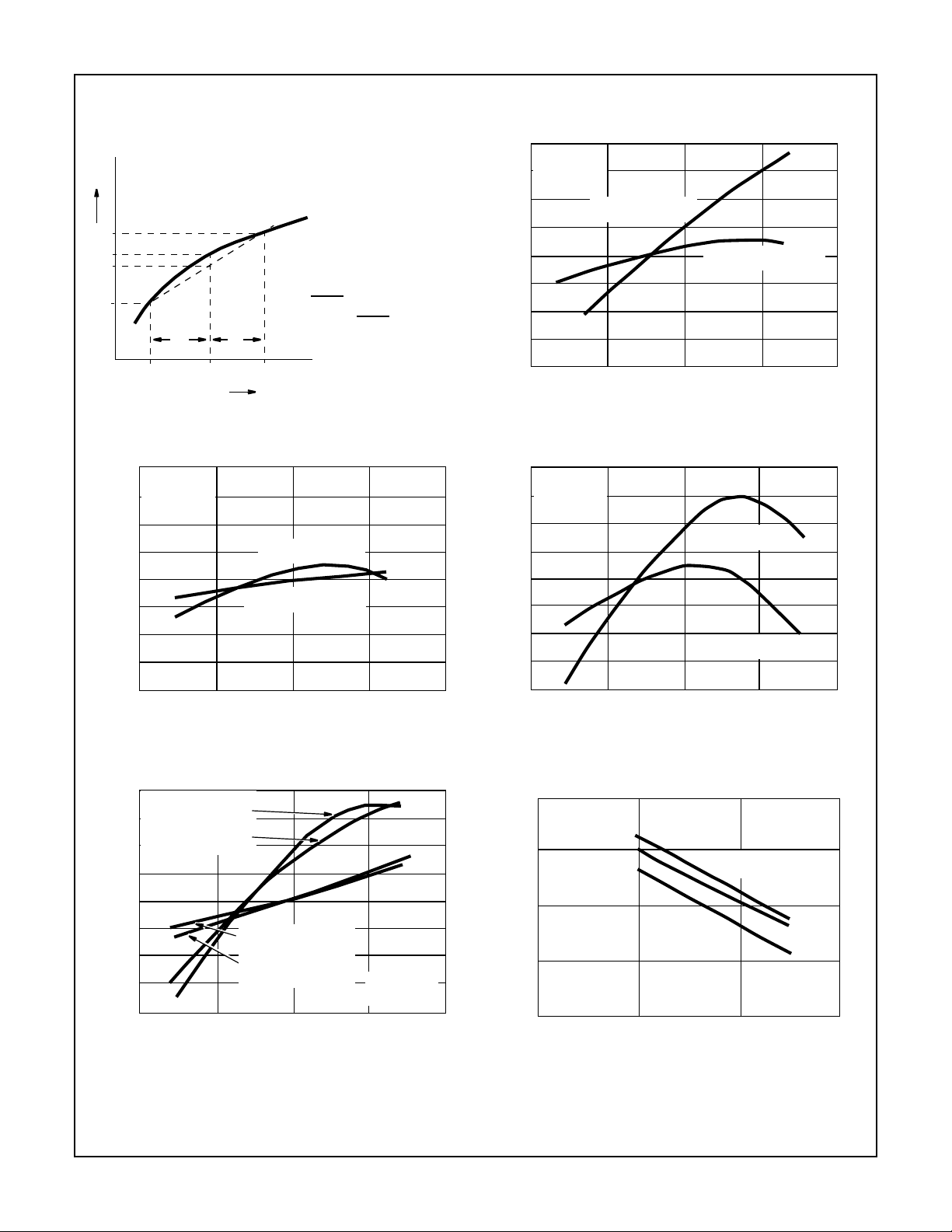
FIGURE 33. DEFINITION OF VCO FREQUENCY LINEARITY FIGURE 34. HC4046A VCO LINEARITY vs R1 (VCC = 4.5V)
4
2
0
-2
LINEARITY (%)
-4
-6
-8
1K 10K
VCOIN = 2.25V ± 1V
VCOIN = 2.25V ± 0.45V
100K 1M 10M
R1 (OHMS)
8
C1 = 50pF
V
= 3V
6
CC
R2 = OPEN
4
2
0
-2
LINEARITY (%)
-4
-6
-8
1K 10K
VCOIN = 1.50V ± 0.4V
VCOIN = 1.50V ± 0.3V
100K 1M 10M
R1 (OHMS)
8
C1 = 50pF
= 6V
V
6
CC
R2 = OPEN
4
2
0
-2
LINEARITY (%)
-4
-6
-8
1K 10K
VCOIN = 3V ± 1.5V
VCOIN = 3V ± 0.6V
100K 1M 10M
R1 (OHMS)
FIGURE 35. HC4046A VCO LINEARITY vs R1 (VCC = 3V) FIGURE 36. HC4046A VCO LINEARITY vs R1 (VCC = 6V)
8
VCC = 5.5V,
VCOIN = 2.75V ±1.3V
6
V
= 4.5V,
CC
= 2.25V ±1.0V
VCO
IN
4
2
0
-2
LINEARITY (%)
-4
-6
-8
1K 10K
FIGURE 37. HCT4046A VCO LINEARITY vs R1 (VCC = 4.5V,
VCC = 5.5V,
= 2.75V ±0.55V
VCO
IN
V
= 4.5V,
CC
VCO
= 2.25V ±0.45V
IN
100K 1M 10M
R1 (OHMS)
C1 = 50pF
R2 = OPEN
VCC = 5.5V)
4
10
(µW)
VCOIN = 0.5 V
D
3
10
2
10
10
1
1K 10K
DEMODULATOR POWER DISSIPATION, P
CC
VCC = 3V
RS (OHMS)
VCC = 6V
VCC = 4.5V
100K 1M
FIGURE 38. HC4046A DEMODULATOR POWER DISSIPATION
vs RS (TYP) (VCC = 3V, 4.5V, 6V)
17
Page 18
CD54HC4046A, CD74HC4046A, CD54HCT4046A, CD74HCT4046A
Typical Performance Curves (Continued)
4
10
(µW)
VCOIN = 0.5 V
D
R1 = R2 = OPEN
3
10
2
10
10
1
DEMODULATOR POWER DISSIPATION, P
1K 10K
CC
VCC = 3V
RS (OHMS)
VCC = 6V
VCC = 4.5V
100K 1M
6
10
VCOIN = 0.5V
R2 = RS = OPEN
C
= 50pF
(µW)
D
L
5
10
4
10
VCC = 3V
C1 = 1µF
3
10
VCO POWER DISSIPATION, P
2
10
1K 10K
CC
VCC = 3V
C1 = 50pF
VCC = 6V
C1 = 50pF
VCC = 4.5V
C1 = 1µF
R1 (OHMS)
VCC = 6V
C1 = 1µF
VCC = 4.5V
C1 = 50pF
100K 1M
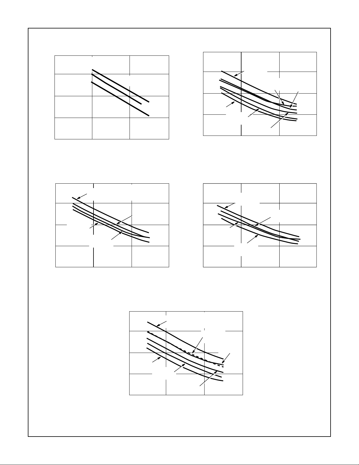
FIGURE 39. HCT4046A DEMODULATOR POWER DISSIPATION
vs RS (TYP) (VCC = 3V, 4.5V, 6V)
6
(µW)
10
VCC = 6V
C1 = 50pF
D
5
10
VCOIN = 0V (AT f
R1 = RS = OPEN
= 50pF
C
L
MIN
)
VCC = 4.5V
4
10
VCC = 4.5V
C1 = 50pF
C1 = 1µF
VCC = 6V
3
10
C1 = 1µF
VCO POWER DISSIPATION, P
2
10
1K 10K
100K 1M
R2 (OHMS)
FIGURE 41. HCT4046A VCO POWER DISSIPATION vs R2
(C1 = 50pF, 1µF)
6
10
VCC = 6V
(µW)
D
5
10
4
10
VCC = 3V
C1 = 1µF
3
10
VCO POWER DISSIPATION, P
2
10
1K 10K
C1 = 50pF
VCC = 3V
C1 = 50pF
FIGURE 40. HC4046A VCO POWER DISSIPATION vs R1
(C1 = 50pF, 1µF)
6
(µW)
10
VCC = 5.5V
D
5
10
C1 = 50pF
VCOIN = 0.5V
R2 = RS = OPEN
VCC = 4.5V
C1 = 50pF
4
10
VCC = 5.5V
C1 = 1µF
3
10
VCC = 4.5V
C1 = 1µF
VCO POWER DISSIPATION, P
2
10
1K 10K
100K 1M
R1 (OHMS)
FIGURE 42. HCT4046A VCO POWER DISSIPATION vs R1
(C1 = 50pF, 1µF)
VCC = 4.5V
C1 = 1µF
R2 (OHMS)
VCOIN = 0V (AT f
R1 = RS = OPEN
= 50pF
C
L
VCC = 4.5V
C1 = 50pF
100K 1M
MIN
VCC = 6V
C1 = 1µF
)
FIGURE 43. HC4046A VCO POWER DISSIPATION vs R2 (C1 = 50pF, 1µF)
18
Page 19
CD54HC4046A, CD74HC4046A, CD54HCT4046A, CD74HCT4046A
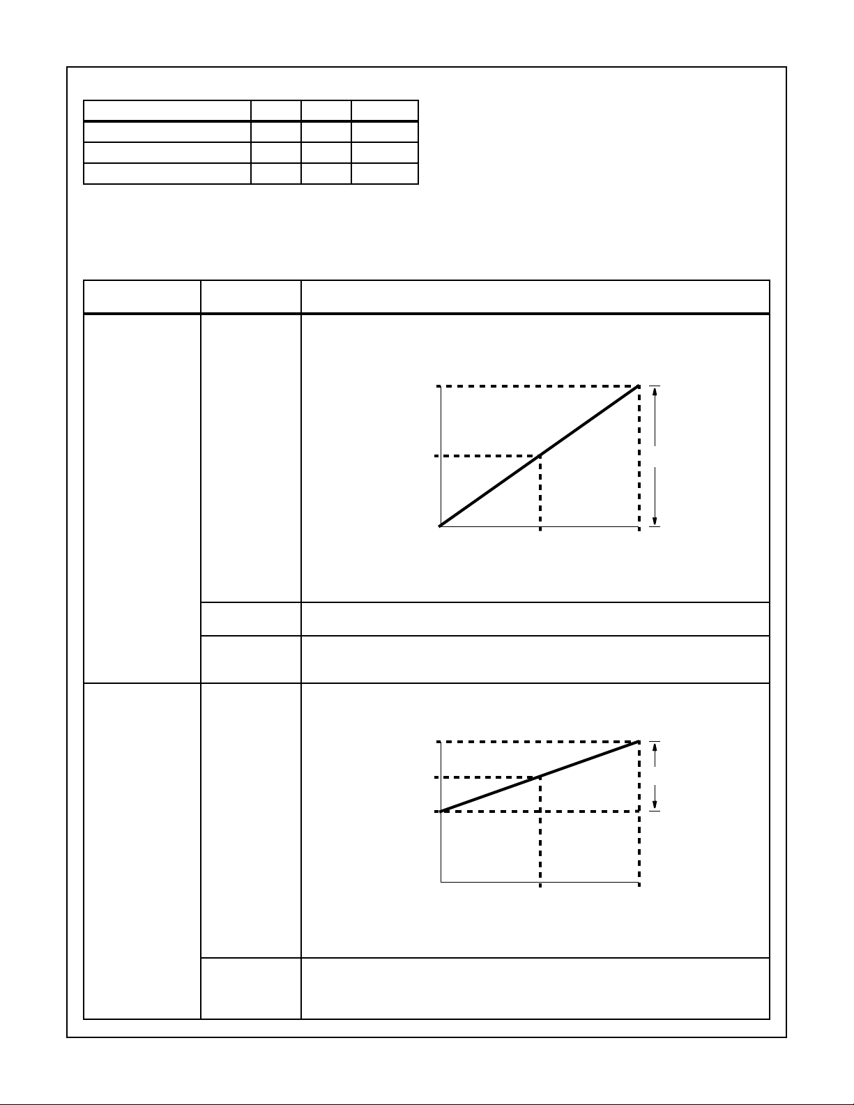
HC/HCT4046A C
PD
CHIP SECTION HC HCT UNIT
Comparator 1 48 50 pF
Comparators 2 and 3 39 48 pF
VCO 61 53 pF
Application Information
This information is a guide for the approximation of values of
external components to be used with the ’HC4046A and
’HCT4046A in a phase-lock-loop system.
PHASE
SUBJECT
VCO Frequency
Without Extra Offset
COMPARATOR DESIGN CONSIDERATIONS
PC1, PC2 or PC3 VCO Frequency Characteristic
With R2 = ∞ and R1 within the range 3kΩ < R1 < 300kΩ, the characteristics of the VCO
operation will be as shown in Figures 11 - 15. (Due to R1, C1 time constant a small offset
remains when R2 = ∞.)
f
f
References should be made to Figures 11 through 15 and
Figures 27 through 32 as indicated in the table.
Values of the selected components should be within the
following ranges:
R1 Between 3kΩ and 300kΩ
R2 Between 3kΩ and 300kΩ
R1 + R2 Parallel Value > 2.7kΩ
C1 Greater Than 40pF
MAX
VCO
f
o
2f
L
VCO Frequency with
Extra Offset
f
MIN
MIN
FIGURE 44. FREQUENCY CHARACTERISTIC OF VCO OPERATING WITHOUT
OFFSET: fo = CENTER FREQUENCY: 2fL = FREQUENCY LOCK RANGE
PC1 Selection of R1 and C1
Given fo, determine the values of R1 and C1 using Figures 11 - 15
PC2 or PC3 Given f
15. To obtain 2fL:2f
calculate foas f
MAX
≈1.2 (V
L
MAX
< VCC - 0.9V
PC1, PC2 or PC3 VCO Frequency Characteristic
With R1 and R2 within the ranges 3kΩ < R1 < 300kΩ,3kΩ, < R2 < 300kΩ, the characteristics
of the VCO operation will be as shown in Figures 27 - 32.
f
MAX
f
VCO
f
o
f
MIN
MIN
FIGURE 45. FREQUENCY CHARACTERISTIC OF VCO OPERATING WITH OFFSET:
fo = CENTER FREQUENCY: 2fL = FREQUENCY LOCK RANGE
V
1/2 V
CC
VCOIN
MAX
/2 and determine the values of R1 and C1 using Figures 11 -
- 1.8V)/(R1C1) where valid range of VCOINis 1.1V < VCO
CC
2f
L
CC
V
VCOIN
MAX
1/2 V
IN
PC1, PC2 or PC3 Selection of R1, R2 and C1
Given fo and fL, offset frequency, f
Obtain the values of C1 and R2 by using Figures 27 - 30.
Calculate the values of R1 from Figures 31 - 32.
19
, may be calculated from f
MIN
MIN
≈ f
- 1.6 fL.
o
Page 20
A
CD54HC4046A, CD74HC4046A, CD54HCT4046A, CD74HCT4046A
SUBJECT
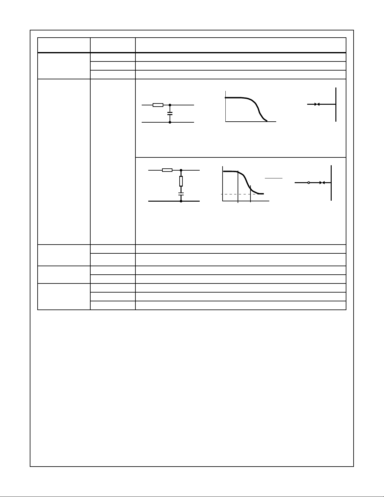
PLL Conditions with
No Signal at the
SIGIN Input
PLL Frequency
Capture Range
PHASE
COMPARATOR DESIGN CONSIDERATIONS
PC1 VCO adjusts to fo with φ
PC2 VCO adjusts to f
PC3 VCO adjusts to f
MIN
MAX
with φ
with φ
DEMOUT
= 90o and V
DEMOUT
DEMOUT
VCOIN
= -360o and V
= 360o and V
= 1/2 VCC (see Figure 2)
= 0V (see Figure 4)
VCOIN
= VCC (see Figure 6)
VCOIN
PC1, PC2 or PC3 Loop Filter Component Selection
|F
|
R3
C2
INPUT OUTPUT
(jω)
ω
(A) τ = R3 x C2
small capture range (2fc) is obtained if τ > 2f
FIGURE 46. SIMPLE LOOP FILTER FOR PLL WITHOUT OFFSET
R3
INPUT OUTPUT
R4
C2
(B) AMPLITUDE CHARACTERISTIC (C) POLE-ZERO DIAGRAM
≈ 1/π (2πf
c
|F
|
(jω)
m
m =
/τ.)
L
R4
R3 + R4
1/2
-1/
-1/
τ
-1/
2
3
τ
τ
PLL Locks on
Harmonics at Center
Frequency
Noise Rejection at
Signal Input
AC Ripple Content
when PLL is Locked
(A) τ1 = R3 x C2;
(B) AMPLITUDE CHARACTERISTIC (C) POLE-ZERO DIAGRAM
τ2 = R4 x C2;
τ3 = (R3 + R4) x C2
FIGURE 47. SIMPLE LOOP FILTER FOR PLL WITH OFFSET
PC1 or PC3 Yes
PC2 No
PC1 High
PC2 or PC3 Low
PC1 fr = 2fi, large ripple content at φ
PC2 fr = fi, small ripple content at φ
PC3 fr = fSIGIN, large ripple content at φ
DEMOUT
DEMOUT
= 90
= 0
DEMOUT
1/
τ
o
o
= 180
1/
3
ω
2
τ
o
20
Page 21
PACKAGE OPTION ADDENDUM
www.ti.com
PACKAGING INFORMATION
Orderable Device Status
5962-8875701EA ACTIVE CDIP J 16 1 TBD SNPB N / A for Pkg Type -55 to 125 5962-8875701EA
5962-8960901EA ACTIVE CDIP J 16 1 TBD SNPB N / A for Pkg Type -55 to 125 5962-8960901EA
CD54HC4046AF ACTIVE CDIP J 16 1 TBD SNPB N / A for Pkg Type -55 to 125 CD54HC4046AF
CD54HC4046AF3A ACTIVE CDIP J 16 1 TBD SNPB N / A for Pkg Type -55 to 125 5962-8960901EA
CD54HCT4046AF3A ACTIVE CDIP J 16 1 TBD SNPB N / A for Pkg Type -55 to 125 5962-8875701EA
CD74HC4046AE ACTIVE PDIP N 16 25 Green (RoHS
CD74HC4046AM ACTIVE SOIC D 16 40 Green (RoHS
CD74HC4046AM96 ACTIVE SOIC D 16 2500 Green (RoHS
CD74HC4046AM96E4 ACTIVE SOIC D 16 2500 Green (RoHS
CD74HC4046AM96G4 ACTIVE SOIC D 16 2500 Green (RoHS
CD74HC4046AMG4 ACTIVE SOIC D 16 40 Green (RoHS
CD74HC4046AMT ACTIVE SOIC D 16 250 Green (RoHS
CD74HC4046ANSR ACTIVE SO NS 16 2000 Green (RoHS
CD74HC4046ANSRE4 ACTIVE SO NS 16 2000 Green (RoHS
CD74HC4046APWR ACTIVE TSSOP PW 16 2000 Green (RoHS
CD74HC4046APWRE4 ACTIVE TSSOP PW 16 2000 Green (RoHS
Package Type Package
(1)
Drawing
Pins Package
Qty
Eco Plan
(2)
& no Sb/Br)
& no Sb/Br)
& no Sb/Br)
& no Sb/Br)
& no Sb/Br)
& no Sb/Br)
& no Sb/Br)
& no Sb/Br)
& no Sb/Br)
& no Sb/Br)
& no Sb/Br)
Lead finish/
Ball material
(6)
MSL Peak Temp
(3)
Op Temp (°C) Device Marking
CD54HCT4046AF3
A
CD54HC4046AF3A
CD54HC4046AF3A
CD54HCT4046AF3
A
NIPDAU N / A for Pkg Type -55 to 125 CD74HC4046AE
NIPDAU Level-1-260C-UNLIM -55 to 125 HC4046AM
NIPDAU Level-1-260C-UNLIM -55 to 125 HC4046AM
NIPDAU Level-1-260C-UNLIM -55 to 125 HC4046AM
NIPDAU Level-1-260C-UNLIM -55 to 125 HC4046AM
NIPDAU Level-1-260C-UNLIM -55 to 125 HC4046AM
NIPDAU Level-1-260C-UNLIM -55 to 125 HC4046AM
NIPDAU Level-1-260C-UNLIM -55 to 125 HC4046AM
NIPDAU Level-1-260C-UNLIM -55 to 125 HC4046AM
NIPDAU Level-1-260C-UNLIM -55 to 125 HJ4046A
NIPDAU Level-1-260C-UNLIM -55 to 125 HJ4046A
28-Jul-2020
Samples
(4/5)
Addendum-Page 1
Page 22
PACKAGE OPTION ADDENDUM
www.ti.com
Orderable Device Status
CD74HC4046APWT ACTIVE TSSOP PW 16 250 Green (RoHS
CD74HCT4046AE ACTIVE PDIP N 16 25 Green (RoHS
CD74HCT4046AEE4 ACTIVE PDIP N 16 25 Green (RoHS
CD74HCT4046AM ACTIVE SOIC D 16 40 Green (RoHS
CD74HCT4046AM96 ACTIVE SOIC D 16 2500 Green (RoHS
CD74HCT4046AM96E4 ACTIVE SOIC D 16 2500 Green (RoHS
CD74HCT4046AMG4 ACTIVE SOIC D 16 40 Green (RoHS
CD74HCT4046AMT ACTIVE SOIC D 16 250 Green (RoHS
(1)
The marketing status values are defined as follows:
ACTIVE: Product device recommended for new designs.
LIFEBUY: TI has announced that the device will be discontinued, and a lifetime-buy period is in effect.
NRND: Not recommended for new designs. Device is in production to support existing customers, but TI does not recommend using this part in a new design.
PREVIEW: Device has been announced but is not in production. Samples may or may not be available.
OBSOLETE: TI has discontinued the production of the device.
Package Type Package
(1)
Drawing
Pins Package
Qty
Eco Plan
(2)
& no Sb/Br)
& no Sb/Br)
& no Sb/Br)
& no Sb/Br)
& no Sb/Br)
& no Sb/Br)
& no Sb/Br)
& no Sb/Br)
Lead finish/
Ball material
(6)
NIPDAU Level-1-260C-UNLIM -55 to 125 HJ4046A
NIPDAU N / A for Pkg Type -55 to 125 CD74HCT4046AE
NIPDAU N / A for Pkg Type -55 to 125 CD74HCT4046AE
NIPDAU Level-1-260C-UNLIM -55 to 125 HCT4046AM
NIPDAU Level-1-260C-UNLIM -55 to 125 HCT4046AM
NIPDAU Level-1-260C-UNLIM -55 to 125 HCT4046AM
NIPDAU Level-1-260C-UNLIM -55 to 125 HCT4046AM
NIPDAU Level-1-260C-UNLIM -55 to 125 HCT4046AM
MSL Peak Temp
(3)
Op Temp (°C) Device Marking
(4/5)
(2)
RoHS: TI defines "RoHS" to mean semiconductor products that are compliant with the current EU RoHS requirements for all 10 RoHS substances, including the requirement that RoHS substance
do not exceed 0.1% by weight in homogeneous materials. Where designed to be soldered at high temperatures, "RoHS" products are suitable for use in specified lead-free processes. TI may
reference these types of products as "Pb-Free".
RoHS Exempt: TI defines "RoHS Exempt" to mean products that contain lead but are compliant with EU RoHS pursuant to a specific EU RoHS exemption.
Green: TI defines "Green" to mean the content of Chlorine (Cl) and Bromine (Br) based flame retardants meet JS709B low halogen requirements of <=1000ppm threshold. Antimony trioxide based
flame retardants must also meet the <=1000ppm threshold requirement.
(3)
MSL, Peak Temp. - The Moisture Sensitivity Level rating according to the JEDEC industry standard classifications, and peak solder temperature.
(4)
There may be additional marking, which relates to the logo, the lot trace code information, or the environmental category on the device.
28-Jul-2020
Samples
Addendum-Page 2
Page 23
PACKAGE OPTION ADDENDUM
www.ti.com
(5)
Multiple Device Markings will be inside parentheses. Only one Device Marking contained in parentheses and separated by a "~" will appear on a device. If a line is indented then it is a continuation
of the previous line and the two combined represent the entire Device Marking for that device.
(6)
Lead finish/Ball material - Orderable Devices may have multiple material finish options. Finish options are separated by a vertical ruled line. Lead finish/Ball material values may wrap to two
lines if the finish value exceeds the maximum column width.
Important Information and Disclaimer:The information provided on this page represents TI's knowledge and belief as of the date that it is provided. TI bases its knowledge and belief on information
provided by third parties, and makes no representation or warranty as to the accuracy of such information. Efforts are underway to better integrate information from third parties. TI has taken and
continues to take reasonable steps to provide representative and accurate information but may not have conducted destructive testing or chemical analysis on incoming materials and chemicals.
TI and TI suppliers consider certain information to be proprietary, and thus CAS numbers and other limited information may not be available for release.
In no event shall TI's liability arising out of such information exceed the total purchase price of the TI part(s) at issue in this document sold by TI to Customer on an annual basis.
OTHER QUALIFIED VERSIONS OF CD54HC4046A, CD54HCT4046A, CD74HC4046A, CD74HCT4046A :
Catalog: CD74HC4046A, CD74HCT4046A
•
Military: CD54HC4046A, CD54HCT4046A
•
NOTE: Qualified Version Definitions:
Catalog - TI's standard catalog product
•
28-Jul-2020
Military - QML certified for Military and Defense Applications
•
Addendum-Page 3
Page 24
PACKAGE MATERIALS INFORMATION
www.ti.com 16-Oct-2020
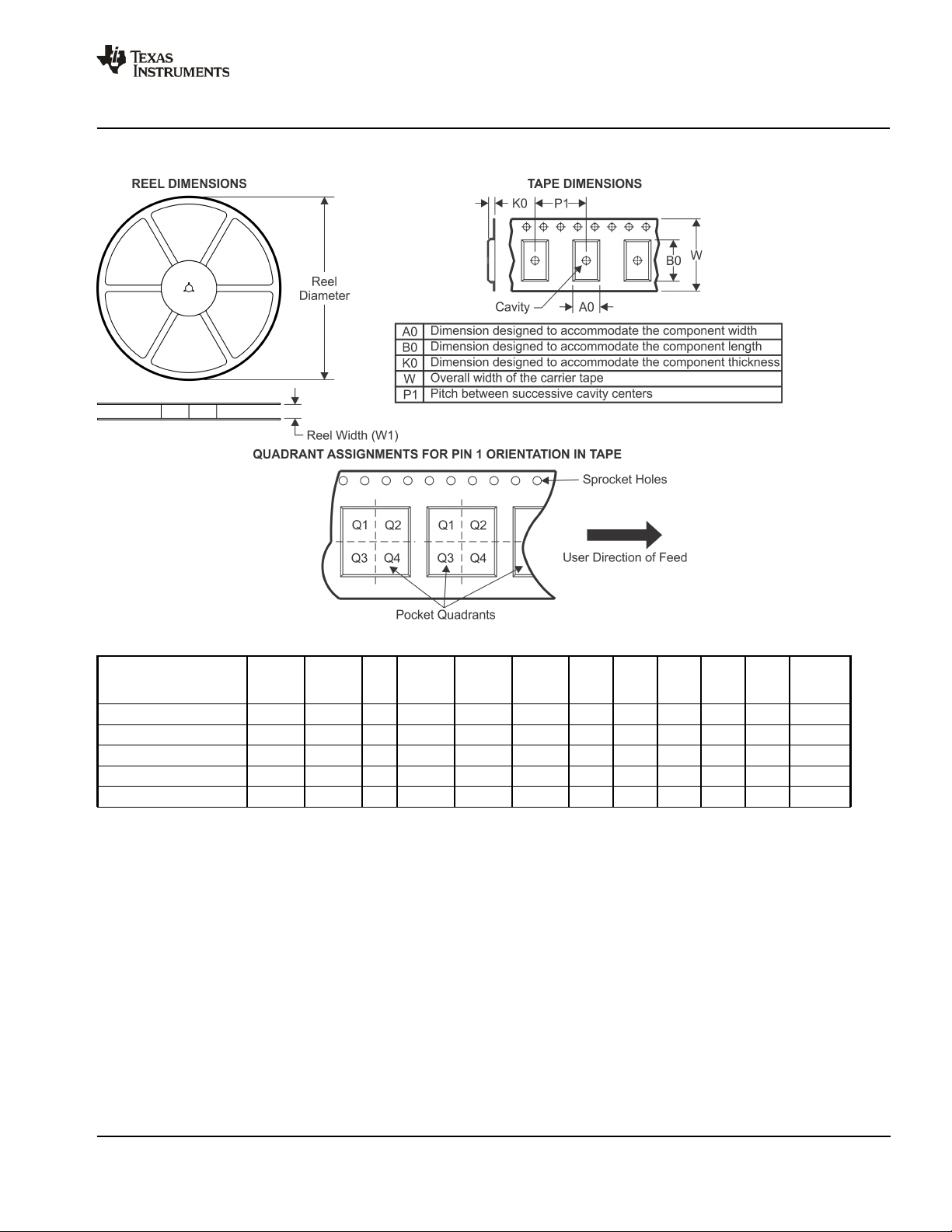
TAPE AND REEL INFORMATION
*All dimensions are nominal
Device Package
CD74HC4046AM96 SOIC D 16 2500 330.0 16.4 6.5 10.3 2.1 8.0 16.0 Q1
CD74HC4046ANSR SO NS 16 2000 330.0 16.4 8.2 10.5 2.5 12.0 16.0 Q1
CD74HC4046APWR TSSOP PW 16 2000 330.0 12.4 6.9 5.6 1.6 8.0 12.0 Q1
CD74HC4046APWT TSSOP PW 16 250 330.0 12.4 6.9 5.6 1.6 8.0 12.0 Q1
CD74HCT4046AM96 SOIC D 16 2500 330.0 16.4 6.5 10.3 2.1 8.0 16.0 Q1
Type
Package
Drawing
Pins SPQ Reel
Diameter
(mm)
Reel
Width
W1 (mm)
A0
(mm)B0(mm)K0(mm)P1(mm)W(mm)
Pin1
Quadrant
Pack Materials-Page 1
Page 25
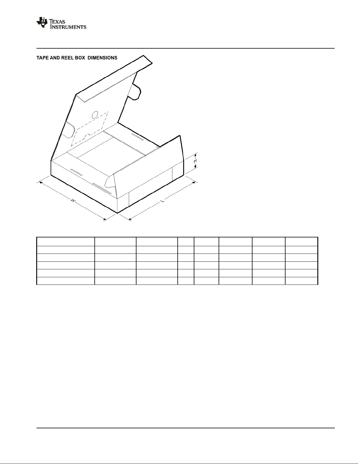
PACKAGE MATERIALS INFORMATION
www.ti.com 16-Oct-2020
*All dimensions are nominal
Device Package Type Package Drawing Pins SPQ Length (mm) Width (mm) Height (mm)
CD74HC4046AM96 SOIC D 16 2500 333.2 345.9 28.6
CD74HC4046ANSR SO NS 16 2000 367.0 367.0 38.0
CD74HC4046APWR TSSOP PW 16 2000 853.0 449.0 35.0
CD74HC4046APWT TSSOP PW 16 250 853.0 449.0 35.0
CD74HCT4046AM96 SOIC D 16 2500 333.2 345.9 28.6
Pack Materials-Page 2
Page 26
Page 27
Page 28
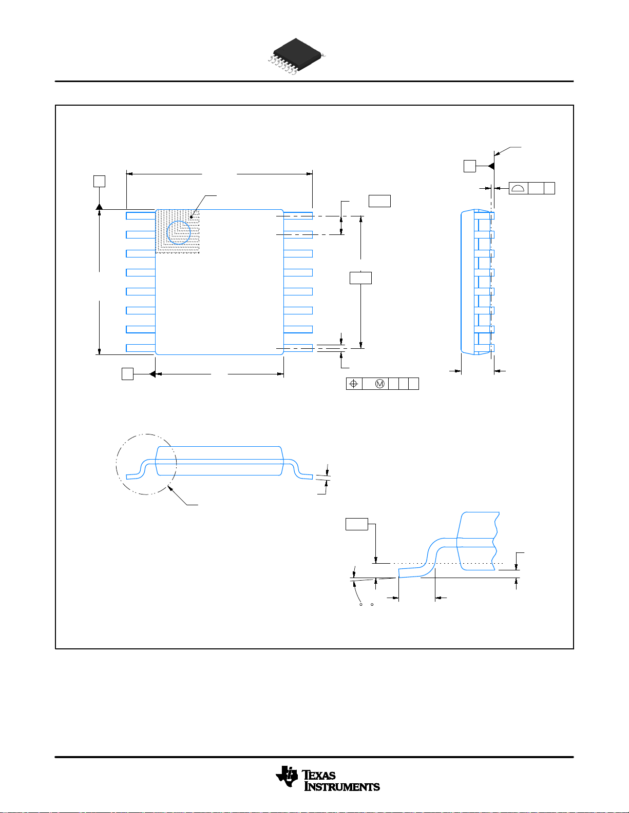
PACKAGE OUTLINE
A
5.1
4.9
NOTE 3
SCALE 2.500
TSSOP - 1.2 mm max heightPW0016A
SMALL OUTLINE PACKAGE
SEATING
6.6
TYP
6.2
PIN 1 INDEX AREA
1
8
B
4.5
4.3
NOTE 4
16
9
14X 0.65
2X
4.55
0.30
16X
0.19
0.1 C A B
C
1.2 MAX
PLANE
0.1 C
(0.15) TYP
SEE DETAIL A
GAGE PLANE
0.25
0.75
-80
0.50
A 20
DETAIL A
TYPICAL
4220204/A 02/2017
NOTES:
1. All linear dimensions are in millimeters. Any dimensions in parenthesis are for reference only. Dimensioning and tolerancing
per ASME Y14.5M.
2. This drawing is subject to change without notice.
3. This dimension does not include mold flash, protrusions, or gate burrs. Mold flash, protrusions, or gate burrs shall not
exceed 0.15 mm per side.
4. This dimension does not include interlead flash. Interlead flash shall not exceed 0.25 mm per side.
5. Reference JEDEC registration MO-153.
0.15
0.05
www.ti.com
Page 29
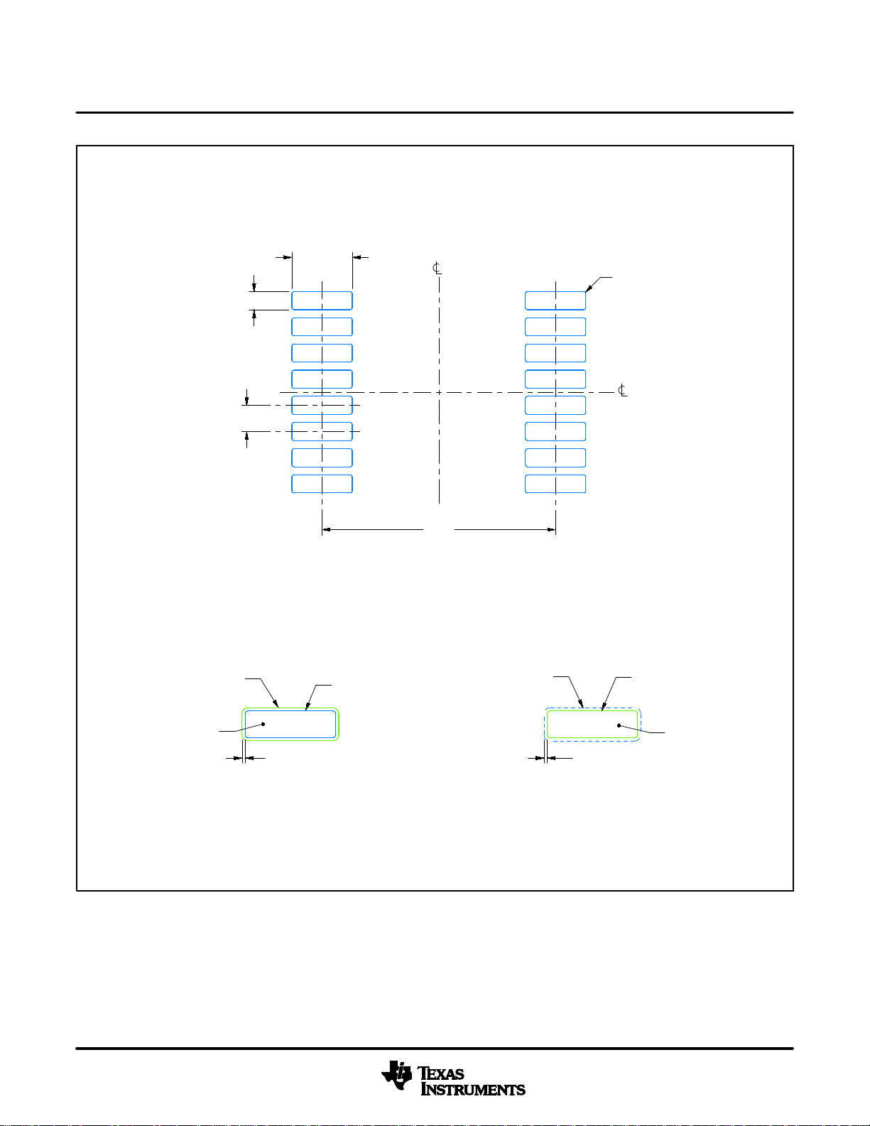
EXAMPLE BOARD LAYOUT
TSSOP - 1.2 mm max heightPW0016A
SMALL OUTLINE PACKAGE
16X (0.45)
14X (0.65)
1
8
16X (1.5)
SYMM
(R0.05) TYP
16
SYMM
9
(5.8)
LAND PATTERN EXAMPLE
EXPOSED METAL SHOWN
SCALE: 10X
SOLDER MASK
OPENING
EXPOSED METAL
0.05 MAX
ALL AROUND
NON-SOLDER MASK
DEFINED
(PREFERRED)
METAL
15.000
SOLDER MASK DETAILS
METAL UNDER
SOLDER MASK
0.05 MIN
ALL AROUND
SOLDER MASK
DEFINED
NOTES: (continued)
6. Publication IPC-7351 may have alternate designs.
7. Solder mask tolerances between and around signal pads can vary based on board fabrication site.
SOLDER MASK
OPENING
EXPOSED METAL
4220204/A 02/2017
www.ti.com
Page 30
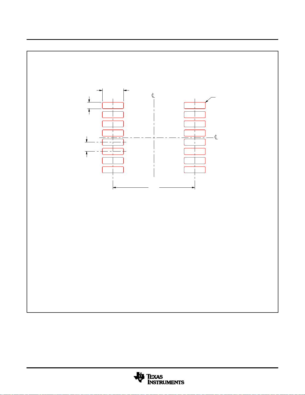
EXAMPLE STENCIL DESIGN
TSSOP - 1.2 mm max heightPW0016A
SMALL OUTLINE PACKAGE
16X (0.45)
14X (0.65)
1
8
16X (1.5)
SYMM
(5.8)
SOLDER PASTE EXAMPLE
BASED ON 0.125 mm THICK STENCIL
SCALE: 10X
(R0.05) TYP
16
SYMM
9
4220204/A 02/2017
NOTES: (continued)
8. Laser cutting apertures with trapezoidal walls and rounded corners may offer better paste release. IPC-7525 may have alternate
design recommendations.
9. Board assembly site may have different recommendations for stencil design.
www.ti.com
Page 31
Page 32
Page 33
Page 34

IMPORTANT NOTICE AND DISCLAIMER
TI PROVIDES TECHNICAL AND RELIABILITY DATA (INCLUDING DATASHEETS), DESIGN RESOURCES (INCLUDING REFERENCE
DESIGNS), APPLICATION OR OTHER DESIGN ADVICE, WEB TOOLS, SAFETY INFORMATION, AND OTHER RESOURCES “AS IS”
AND WITH ALL FAULTS, AND DISCLAIMS ALL WARRANTIES, EXPRESS AND IMPLIED, INCLUDING WITHOUT LIMITATION ANY
IMPLIED WARRANTIES OF MERCHANTABILITY, FITNESS FOR A PARTICULAR PURPOSE OR NON-INFRINGEMENT OF THIRD
PARTY INTELLECTUAL PROPERTY RIGHTS.
These resources are intended for skilled developers designing with TI products. You are solely responsible for (1) selecting the appropriate
TI products for your application, (2) designing, validating and testing your application, and (3) ensuring your application meets applicable
standards, and any other safety, security, or other requirements. These resources are subject to change without notice. TI grants you
permission to use these resources only for development of an application that uses the TI products described in the resource. Other
reproduction and display of these resources is prohibited. No license is granted to any other TI intellectual property right or to any third
party intellectual property right. TI disclaims responsibility for, and you will fully indemnify TI and its representatives against, any claims,
damages, costs, losses, and liabilities arising out of your use of these resources.
TI’s products are provided subject to TI’s Terms of Sale (www.ti.com/legal/termsofsale.html) or other applicable terms available either on
ti.com or provided in conjunction with such TI products. TI’s provision of these resources does not expand or otherwise alter TI’s applicable
warranties or warranty disclaimers for TI products.
Mailing Address: Texas Instruments, Post Office Box 655303, Dallas, Texas 75265
Copyright © 2020, Texas Instruments Incorporated
 Loading...