

Page 1

DATA SH EET
Product specification
File under Integrated Circuits, IC06
December 1990
INTEGRATED CIRCUITS
74HC/HCT237
3-to-8 line decoder/demultiplexer
with address latches
For a complete data sheet, please also download:
•The IC06 74HC/HCT/HCU/HCMOS Logic Family Specifications
•The IC06 74HC/HCT/HCU/HCMOS Logic Package Information
•The IC06 74HC/HCT/HCU/HCMOS Logic Package Outlines
Page 2
December 1990 2
Philips Semiconductors Product specification
3-to-8 line decoder/demultiplexer with
address latches
74HC/HCT237
FEATURES
• Combines 3-to-8 decoder with 3-bit latch
• Multiple input enable for easy expansion or independent
controls
• Active HIGH mutually exclusive outputs
• Output capability: standard
• ICC category: MSI
GENERAL DESCRIPTION
The 74HC/HCT237 are high-speed Si-gate CMOS devices
and are pin compatible with low power Schottky TTL
(LSTTL). They are specified in compliance with JEDEC
standard no. 7A.
The 74HC/HCT237 are 3-to-8 line decoder/demultiplexers
with latches at the three address inputs (A
n
). The “237”
essentially combines the 3-to-8 decoder function with a
3-bit storage latch. When the latch is enabled (LE = LOW),
the “237” acts as a 3-to-8 active LOW decoder. When the
latch enable (LE) goes from LOW-to-HIGH, the last data
present at the inputs before this transition, is stored in the
latches. Further address changes are ignored as long as
LE remains HIGH.
The output enable input (E1 and E2) controls the state of
the outputs independent of the address inputs or latch
operation. All outputs are HIGH unless E1 is LOW and E
2
is HIGH.
The “237” is ideally suited for implementing
non-overlapping decoders in 3-state systems and strobed
(stored address) applications in bus oriented systems.
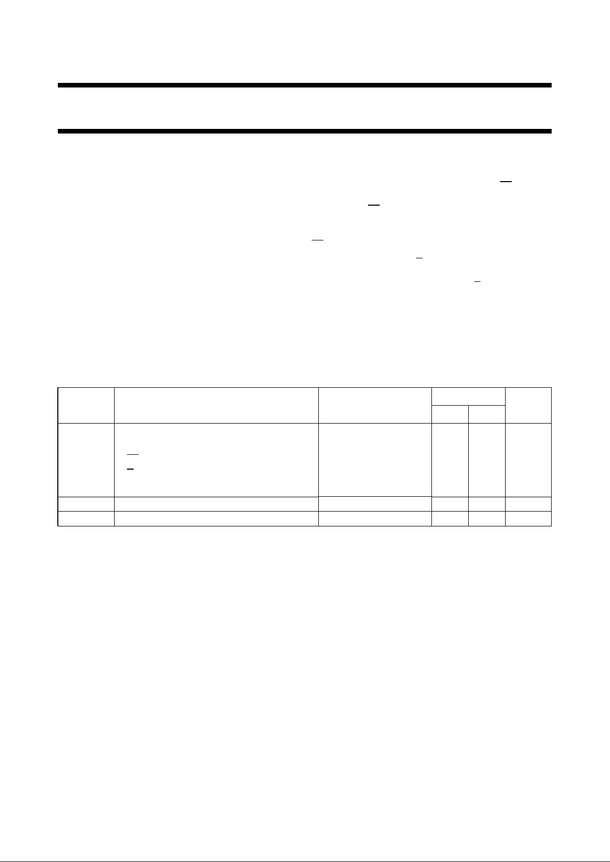
QUICK REFERENCE DATA
GND = 0 V; T
amb
=25°C; tr=tf= 6 ns
Notes
1. C
PD
is used to determine the dynamic power dissipation (PD in µW):
PD=CPD× V
CC
2
× fi+ ∑ (CL× V
CC
2
× fo) where:
fi= input frequency in MHz
fo= output frequency in MHz
∑ (CL× V
CC
2
× fo) = sum of outputs
CL= output load capacitance in pF
VCC= supply voltage in V
2. For HC the condition is VI= GND to V
CC
For HCT the condition is VI= GND to VCC− 1.5 V
ORDERING INFORMATION
See
“74HC/HCT/HCU/HCMOS Logic Package Information”
.
SYMBOL PARAMETER CONDITIONS
TYPICAL
UNIT
HC HCT
t
PHL
/ t
PLH
propagation delay CL= 15 pF; VCC=5 V
A
n
to Y
n
16 19 ns
LE to Y
n
19 21 ns
E1 to Y
n
14 17 ns
E
2
to Y
n
14 17 ns
C
I
input capacitance 3.5 3.5 pF
C
PD
power dissipation capacitance per package notes 1 and 2 60 63 pF
Page 3
December 1990 3
Philips Semiconductors Product specification
3-to-8 line decoder/demultiplexer with
address latches
74HC/HCT237
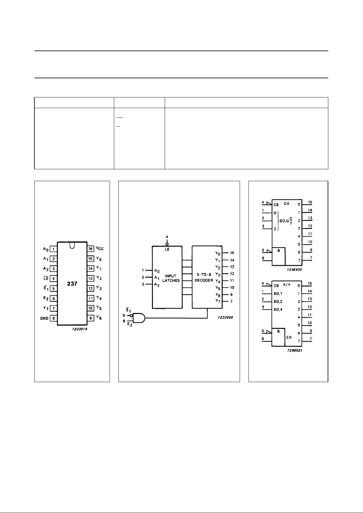
PIN DESCRIPTION
PIN NO. SYMBOL NAME AND FUNCTION
1, 2, 3 A
0
to A
2
data inputs
4
LE latch enable input (active LOW)
5
E
1
data enable input (active LOW)
6E
2
data enable input (active HIGH)
8 GND ground (0 V)
15, 14, 13, 12, 11, 10, 9, 7 Y
0
to Y
7
multiplexer outputs
16 V
CC
positive supply voltage
Fig.1 Pin configuration. Fig.2 Logic symbol. Fig.3 IEC logic symbol.
Page 4

December 1990 4
Philips Semiconductors Product specification
3-to-8 line decoder/demultiplexer with
address latches
74HC/HCT237
FUNCTION TABLE
Notes
1. H = HIGH voltage level
L = LOW voltage level
X = don’t care
INPUTS OUTPUTS
LE E
1
E
2
A
0
A
1
A
2
Y
0
Y
1
Y
2
Y
3
Y
4
Y
5
Y
6
Y
7
H L H X X X stable
XHXXXXLLLLLLLL
XXLXXXLLLLLLLL
LLHLLLHLLLLLLL
LLHHLLLHLLLLLL
LLHLHLLLHLLLLL
LLHHHLLLLHLLLL
LLHLLHLLLLHLLL
LLHHLHLLLLLHLL
LLHLHHLLLLLLHL
LLHHHHLLLLLLLH
Fig.4 Functional diagram.
Page 5

December 1990 5
Philips Semiconductors Product specification
3-to-8 line decoder/demultiplexer with
address latches
74HC/HCT237
Fig.5 Logic diagram.
Page 6

December 1990 6
Philips Semiconductors Product specification
3-to-8 line decoder/demultiplexer with
address latches
74HC/HCT237
DC CHARACTERISTICS FOR 74HC
For the DC characteristics see
“74HC/HCT/HCU/HCMOS Logic Family Specifications”
.
Output capability: standard
ICC category: MSI
AC CHARACTERISTICS FOR 74HC
GND = 0 V; t
r=tf
= 6 ns; CL= 50 pF
SYMBOL PARAMETER
T
amb
(°C)
UNIT
TEST CONDITIONS
74HC
V
CC
(V)
WAVEFORMS
+25 −40 to +85 −40 to +125
min. typ. max. min. max. min. max.
t
PHL
/ t
PLH
propagation delay
An to Y
n
52
19
15
160
32
27
200
40
34
240
48
41
ns 2.0
4.5
6.0
Fig.6
t
PHL
/ t
PLH
propagation delay
LE to Y
n
61
22
18
190
38
32
240
48
41
285
57
48
ns 2.0
4.5
6.0
Fig.7
t
PHL
/ t
PLH
propagation delay
E1 to Y
n
47
17
14
145
29
25
180
36
31
220
44
38
ns 2.0
4.5
6.0
Fig.7
t
PHL
/ t
PLH
propagation delay
E2 to Y
n
47
17
14
145
29
25
180
36
31
220
44
38
ns 2.0
4.5
6.0
Fig.6
t
THL
/ t
TLH
output transition time 19
7
6
75
15
13
95
19
16
110
22
19
ns 2.0
4.5
6.0
Fig.6
t
W
LE pulse width
LOW
50
10
9
11
4
3
65
13
11
75
15
13
ns 2.0
4.5
6.0
Fig.8
t
su
set-up time
An to LE
50
10
9
6
2
2
65
13
11
75
15
13
ns 2.0
4.5
6.0
Fig.8
t
h
hold time
An to LE
30
6
5
3
1
1
40
8
7
45
9
8
ns 2.0
4.5
6.0
Fig.8
Page 7

December 1990 7
Philips Semiconductors Product specification
3-to-8 line decoder/demultiplexer with
address latches
74HC/HCT237
DC CHARACTERISTICS FOR 74HCT
For the DC characteristics see
“74HC/HCT/HCU/HCMOS Logic Family Specifications”
.
Output capability: standard
ICC category: MSI
Note to HCT types
The value of additional quiescent supply current (∆I
CC
) for a unit load of 1 is given in the family specifications.
To determine ∆ICC per input, multiply this value by the unit load coefficient shown in the table below.
AC CHARACTERISTICS FOR 74HCT
GND = 0 V; t
r=tf
= 6 ns; CL= 50 pF
INPUT UNIT LOAD COEFFICIENT
A
n
1.50
E
1
1.50
E
2
1.50
LE 1.50
SYMBOL PARAMETER
T
amb
(°C)
UNIT
TEST CONDITIONS
74HCT
V
CC
(V)
WAVEFORMS
+25 −40 to +85 −40 to +125
min. typ. max. min. max. min. max.
t
PHL
/ t
PLH
propagation delay
An to Y
n
22 38 48 57 ns 4.5 Fig.6
t
PHL
/ t
PLH
propagation delay
LE to Y
n
25 42 53 63 ns 4.5 Fig.7
t
PHL
/ t
PLH
propagation delay
E1 to Y
n
20 35 44 53 ns 4.5 Fig.7
t
PHL
/ t
PLH
propagation delay
E2 to Y
n
20 33 41 50 ns 4.5 Fig.6
t
THL
/ t
TLH
output transition time 7 15 19 22 ns 4.5 Fig.6
t
W
LE pulse width
HIGH
10 5 13 15 ns 4.5 Fig.8
t
su
set-up time
An to LE
10 2 13 15 ns 4.5 Fig.8
t
h
hold time
An to LE
5 0 5 5 ns 4.5 Fig.8
Page 8

December 1990 8
Philips Semiconductors Product specification
3-to-8 line decoder/demultiplexer with
address latches
74HC/HCT237
AC WAVEFORMS
Fig.6 Waveforms showing the address input (An)
and enable inputs (E2, LE) to output (Yn)
propagation delays and the output transition
times.
(1) HC : VM= 50%; VI= GND to VCC.
HCT: V
M
= 1.3 V; VI= GND to 3 V.
Fig.7 Waveforms showing the enable input (E1) to
output (Yn) propagation delays and the
output transition times.
(1) HC : VM= 50%; VI= GND to VCC.
HCT: V
M
= 1.3 V; VI= GND to 3 V.
Fig.8 Waveforms showing the data set-up, hold times for An input to LE input and the latch enable pulse width.
The shaded areas indicate when the input is permitted
to change for predictable output performance.
(1) HC : V
M
= 50%; VI= GND to VCC.
HCT: V
M
= 1.3 V; VI= GND to 3 V.
Page 9

December 1990 9
Philips Semiconductors Product specification
3-to-8 line decoder/demultiplexer with
address latches
74HC/HCT237
APPLICATION INFORMATION
PACKAGE OUTLINES
See
“74HC/HCT/HCU/HCMOS Logic Package Outlines”
.
Fig.9 6-to-64 line decoder with input address storage.
 Loading...