

Page 1

DATA SH EET
Product specification
File under Integrated Circuits, IC06
September 1993
INTEGRATED CIRCUITS
74HC/HCT139
Dual 2-to-4 line
decoder/demultiplexer
For a complete data sheet, please also download:
•The IC06 74HC/HCT/HCU/HCMOS Logic Family Specifications
•The IC06 74HC/HCT/HCU/HCMOS Logic Package Information
•The IC06 74HC/HCT/HCU/HCMOS Logic Package Outlines
Page 2
September 1993 2
Philips Semiconductors Product specification
Dual 2-to-4 line decoder/demultiplexer 74HC/HCT139
FEATURES
• Demultiplexing capability
• Two independent 2-to-4 decoders
• Multifunction capability
• Active LOW mutually exclusive outputs
• Output capability: standard
• ICCcategory: MSI
GENERAL DESCRIPTION
The 74HC/HCT139 are high-speed Si-gate CMOS devices
and are pin compatible with low power Schottky TTL
(LSTTL). It is specified in compliance with JEDEC
standard no. 7A.
The 74HC/HCT139 are high-speed, dual 2-to-4 line
decoder/multiplexers. This device has two independent
decoders, each accepting two binary weighted inputs
(nA0and nA1) and providing four mutually exclusive active
LOW outputs (nY0 to nY3). Each decoder has an active
LOW enable input (nE).
When nE is HIGH, every output is forced HIGH. The
enable can be used as the data input for a 1-to-4
demultiplexer application.
The “139” is identical to the HEF4556 of the HE4000B
family.
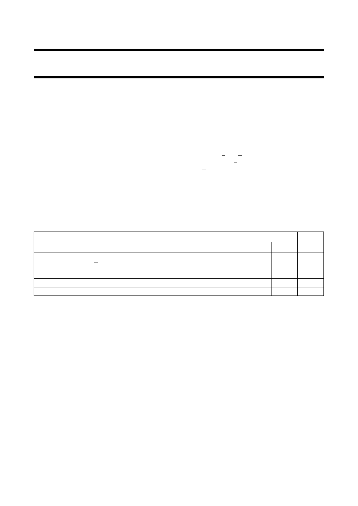
QUICK REFERENCE DATA
GND = 0 V; T
amb
= 25 °C; tr= tf= 6 ns
Notes
1. C
PD
is used to determine the dynamic power dissipation (PDin µW):
PD= CPD× V
CC
2
× fi+∑(CL× V
CC
2
× fo) where:
fi= input frequency in MHz
fo= output frequency in MHz
∑ (CL× V
CC
2
× fo) = sum of outputs
CL= output load capacitance in pF
VCC= supply voltage in V
2. For HC the condition is VI= GND to V
CC
For HCT the condition is VI= GND to VCC− 1.5 V
APPLICATIONS
• Memory decoding or data-routing
• Code conversion
ORDERING INFORMATION
See
“74HC/HCT/HCU/HCMOS Logic Package Information”
.
SYMBOL PARAMETER CONDITIONS
TYPICAL
UNIT
HC HCT
t
PHL
/ t
PLH
propagation delay CL= 15 pF; VCC= 5 V
nA
n
to nY
n
11 13 ns
n
E3to nY
n
10 13 ns
C
I
input capacitance 3.5 3.5 pF
C
PD
power dissipation capacitance per multiplexer notes 1 and 2 42 44 pF
Page 3
September 1993 3
Philips Semiconductors Product specification
Dual 2-to-4 line decoder/demultiplexer 74HC/HCT139
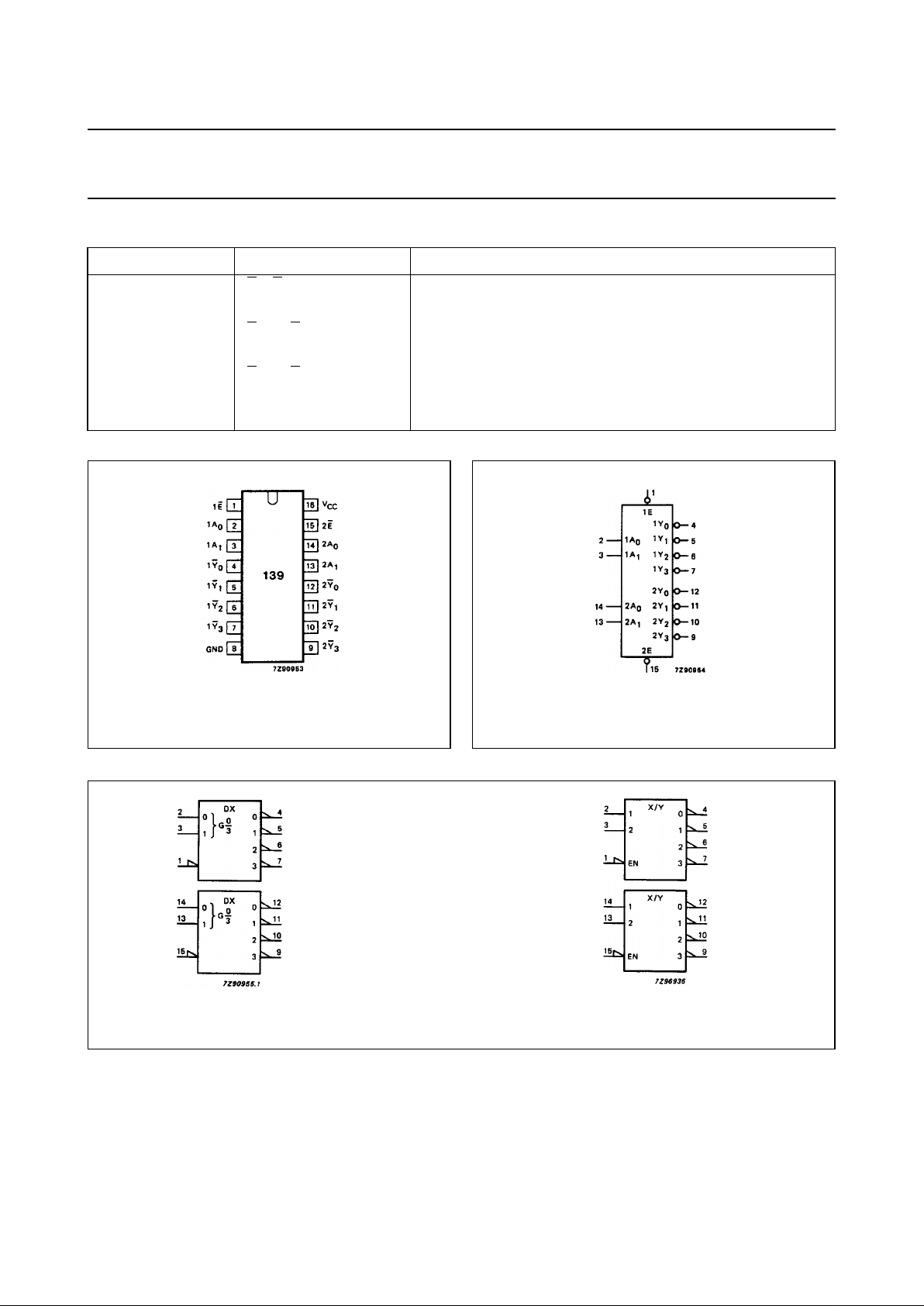
PIN DESCRIPTION
PIN NO. SYMBOL NAME AND FUNCTION
1, 15 1
E, 2E enable inputs (active LOW)
2, 3 1A
0
, 1A
1
address inputs
4, 5, 6, 7 1
Y0to 1Y
3
outputs (active LOW)
8 GND ground (0 V)
12, 11, 10, 9 2
Y0to 2Y
3
outputs (active LOW)
14, 13 2A
0
, 2A
1
address inputs
16 V
CC
positive supply voltage
Fig.1 Pin configuration.
Fig.2 Logic symbol.
Fig.3 IEC logic symbol.
(a) (b)
Page 4

September 1993 4
Philips Semiconductors Product specification
Dual 2-to-4 line decoder/demultiplexer 74HC/HCT139
FUNCTION TABLE
Notes
1. H = HIGH voltage level
L = LOW voltage level
X = don’t care
INPUTS OUTPUTS
nEnA0nA
1
nY
0
nY
1
nY
2
nY
3
HXXHHHH
L
L
L
L
L
H
L
H
L
L
H
H
L
H
H
H
H
L
H
H
H
H
L
H
H
H
H
L
Fig.4 Functional diagram.
Fig.5 Logic diagram (one decoder/demultiplexer).
Page 5

September 1993 5
Philips Semiconductors Product specification
Dual 2-to-4 line decoder/demultiplexer 74HC/HCT139
DC CHARACTERISTICS FOR 74HC
For the DC characteristics see
“74HC/HCT/HCU/HCMOS Logic Family Specifications”
.
Output capability: standard
ICCcategory: MSI
AC CHARACTERISTICS FOR 74HC
GND = 0 V; t
r
= tf= 6 ns; CL= 50 pF
SYMBOL PARAMETER
T
amb
(°C)
UNIT
TEST CONDITIONS
74HC
V
CC
(V)
WAVEFORMS
+25 −40 to +85 −40 to +125
min. typ. max. min. max. min. max.
t
PHL
/ t
PLH
propagation delay
nAnto Y
n
39
14
11
145
29
25
180
36
31
220
44
38
ns
2.0
4.5
6.0
Fig.6
t
PHL
/ t
PLH
propagation delay
nE to nY
n
33
12
10
135
27
23
170
34
29
205
41
35
ns
2.0
4.5
6.0
Fig.7
t
THL
/ t
TLH
output transition
time
19
7
6
75
15
13
95
19
16
110
22
19
ns
2.0
4.5
6.0
Figs 6 and 7
Page 6

September 1993 6
Philips Semiconductors Product specification
Dual 2-to-4 line decoder/demultiplexer 74HC/HCT139
DC CHARACTERISTICS FOR HCT
For the DC characteristics see
“74HC/HCT/HCU/HCMOS Logic Family Specifications”
.
Output capability: standard
ICCcategory: MSI
Note to HCT types
The value of additional quiescent supply current (∆I
CC
) for a unit load of 1 is given in the family specifications.
To determine ∆ICCper input, multiply this value by the unit load coefficient shown in the table below.
AC CHARACTERISTICS FOR 74HCT
GND = 0 V; t
f
= tf= 6 ns; CL= 50 pF
INPUT UNIT LOAD COEFFICIENT
1A
n
2A
n
nE
0.70
0.70
1.35
SYMBOL PARAMETER
T
amb
(°C)
UNIT
TEST CONDITIONS
74HCT
V
CC
(V)
WAVEFORMS
+25 −40 to +85 −40 to +125
min. typ. max. min. max. min. max.
t
PHL
/ t
PLH
propagation delay
nAnto Y
n
16 34 43 51 ns 4.5 Fig.6
t
PHL
/ t
PLH
propagation delay
nE to nY
n
16 34 43 51 ns 4.5 Fig.7
t
THL
/ t
TLH
output transition
time
7 15 19 22 ns 4.5 Figs 6 and 7
Page 7

September 1993 7
Philips Semiconductors Product specification
Dual 2-to-4 line decoder/demultiplexer 74HC/HCT139
AC WAVEFORMS
PACKAGE OUTLINES
See
“74HC/HCT/HCU/HCMOS Logic Package Outlines”
.
Fig.6 Waveforms showing the address input (nAn) to output (nYn) propagation delays and the output transition
times.
(1) HC : VM= 50%; VI= GND to VCC.
HCT: V
M
= 1.3 V; VI= GND to 3 V.
Fig.7 Waveforms showing the enable input (nE) to output (nYn) propagation delays and the output transition
times.
(1) HC : VM= 50%; VI= GND to VCC.
HCT: V
M
= 1.3 V; VI= GND to 3 V.
 Loading...