

Page 1
INTEGRATED CIRCUITS
DATA SH EET
For a complete data sheet, please also download:
•The IC06 74HC/HCT/HCU/HCMOS Logic Family Specifications
•The IC06 74HC/HCT/HCU/HCMOS Logic Package Information
•The IC06 74HC/HCT/HCU/HCMOS Logic Package Outlines
74HC/HCT594
8-bit shift register with output
register
Product specification
File under Integrated Circuits, IC06
December 1991
Page 2
Philips Semiconductors Product specification
8-bit shift register with output register 74HC/HCT594
FEATURES
• Synchronous serial input and output
• 8-bit parallel output
• Shift and storage register have independent direct clear
and clocks
• 100 MHz (typ.)
• Output capability:
– parallel outputs: bus driver
– serial outputs: standard
• ICCcategory: MSI
DESCRIPTION
The 74HC/HCT594 are high-speed, Si-gate CMOS
devices, and are pin compatible with low power Schottky
TTL (LSTTL). They are specified in compliance with
JEDEC standard No. 7A.
The 74HC/HCT594 contain an 8-bit, non-inverting,
serial-in, parallel-out shift register that feeds an 8-bit
D-type storage register. Separate clocks and direct
overriding clears are provided on both the shift and storage
registers. A serial output (Q7’) is provided for cascading
purposes.
Both the shift and storage register clocks are positive-edge
triggered. If the user wishes to connect both clocks
APPLICATIONS
• Serial-to parallel data conversion
together, the shift register will always be one count pulse
ahead of the storage register.
• Remote control holding register
QUICK REFERENCE DATA
GND = 0 V: T
= 250 C; tr = tf= 6 ns.
amb
SYMBOL PARAMETER CONDITIONS
t
PHL/tPLH
f
max
C
I
C
PD
propagation delay CL= 15 pF; VCC= 5 V
SH
to Q7’ 1315ns
CP
ST
to Q
CP
n
SHRto Q
STRto Q
maximum clock frequency SHCP,ST
n
n
CP
input capacitance 3.5 3.5 pF
power dissipation capacitance per package notes 1 and 2 84 89 pF
TYPICAL
UNIT
HC HCT
13 15 ns
11 14 ns
11 14 ns
100 100 MHz
Notes
1. C
is used to determine the dynamic power dissipation (PDin µW).
PD
PD= CPD× V
2
× fi+ ∑ (CL× V
CC
2
× fo), where:
CC
fi= input frequency in MHz; fo= output frequency in MHz;
∑ (CL× V
2
× fo) = sum of the outputs;
CC
CL= output load capacitance in pF; VCC= supply voltage in V.
2. For HC, the condition is VI= GND to VCC; for HCT, the condition is VI= GND to VCC− 1.5 V.
ORDERING INFORMATION
PACKAGES
EXTENDED TYPE NUMBER
PINS PIN POSITION MATERIAL CODE
PC74HC/HCT594P 16 DIL plastic SOT38C, P
PC74HC/HCT594T 16 SO plastic SOT109A
December 1991 2
Page 3
Philips Semiconductors Product specification
8-bit shift register with output register 74HC/HCT594
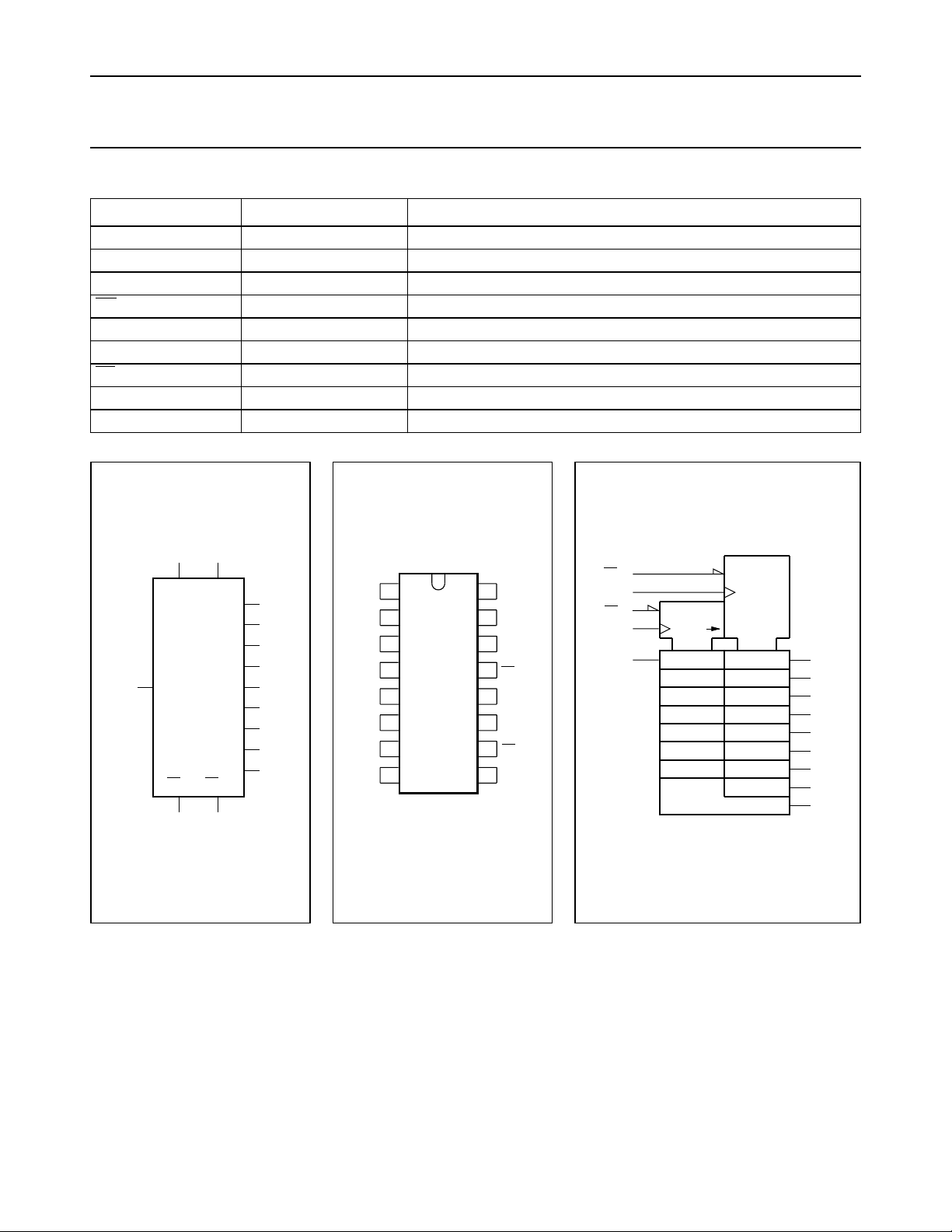
PINNING
SYMBOL PIN DESCRIPTION
Q
to Q
0
7
GND 8 ground (0 V)
Q
’ 9 serial data output
7
SH
R
SH
CP
ST
CP
ST
R
D
s
V
CC
15 & 1 to 7 parallel data outputs
10 shift register reset (active LOW)
11 shift register clock input
12 storage register clock input
13 storage register reset active (LOW)
14 serial data input
16 supply voltage
e
SHCPST
14
D
SHRST
Fig.1 Logic symbol.
11 12
S
10 13
CP
Q7'
Q
Q
Q
Q
Q
Q
Q
Q
R
0
1
2
3
4
5
6
7
MBC319
halfpage
e
9
15
1
2
3
4
5
6
7
Q
Q
Q
Q
Q
Q
Q
GND
1
1
2
2
3
3
4
4
5
6
7
594
5
6
7
8
MBC318
V
16
CC
Q
15
0
14
D
S
13
ST
R
12
ST
CP
SH
11
CP
10
SH
R
9
Q7'
Fig.2 Pin configuration.
13
ST
R
12
ST
CP
10
SH
SH
CP
D
R
11
14
S
R
SRG8
1
C1/
1D 2D
Fig.3 IEC logic symbol.
R
2
C2
MBC322 - 1
15
Q
0
1
Q
1
2
Q
2
3
Q
3
4
Q
4
5
Q
5
6
Q
6
7
Q
7
9
Q7'
December 1991 3
Page 4

Philips Semiconductors Product specification
8-bit shift register with output register 74HC/HCT594
handbook, halfpage
D
S14
SH
CP
11
SH
10
ST
12
ST
13
8-STAGE SHIFT REGISTER
R
CP
8-BIT STORAGE REGISTER
R
Q7'
9
Q0Q1Q2Q3Q4Q5Q6Q
15
1234567
7
MBC320
Fig.4 Functional diagram.
FUNCTION TABLE
INPUTS OUTPUTS
FUNCTION
SHCPST
CP
SH
ST
R
D
R
S
Q7’Q
n
X X L X X L NC a LOW level on SHRonly affects the shift registers.
XXXLXNCLaLOW level on
STRonly affects the storage registers.
X ↑ L H X L L empty shift register loaded into storage register.
↑ XHXHQ
’ NC logic HIGH level shifted into shift register stage 0. Contents of all
6
shift register stages shifted through, e.g. previous state of stage
6 (internal Q6’) appears on the serial output (Q7’).
X ↑ HHXNCQ
’ contents of shift register stages (internal Qn’) are transferred to
n
the storage register and parallel output stages.
↑↑HHXQ
nQn’ contents of shift register shifted through. Previous contents of
6
shift register transferred to the storage register and the parallel
output stages.
Note
1. H = HIGH voltage level
L = LOW voltage level
↑ = LOW-to-HIGH transition
NC = no change
X = don’t care.
December 1991 4
Page 5

Philips Semiconductors Product specification
8-bit shift register with output register 74HC/HCT594
handbook, full pagewidth
SH
SH
D
CP
STAGE 0
D
FFSH
CP
Q
0
R
S
R
STAGES 1 TO
6
DQ
STAGE 7
DQ
FFSH
7
CP
R
Q7'
ST
handbook, full pagewidth
SH
CP
D
S
ST
CP
SH
R
ST
CP
D
Q
FFST
0
CP
R
R
Q
Q1Q2Q3Q4Q5Q
0
6
D
FFST
CP
Q
7
R
Q
7
MBC321 - 1
Fig.5 Logic diagram.
ST
R
Q
0
Q
1
Q
6
Q
7
Q '
7
Fig.6 Timing diagram.
December 1991 5
MBC323 - 1
Page 6

Philips Semiconductors Product specification
8-bit shift register with output register 74HC/HCT594
DC CHARACTERISTICS FOR 74HC
For the DC characteristics, see
“74HC/HCT/HCU/HCMOS Logic Family Specifications”
Output capability: parallel outputs, bus driver; serial output, standard.
ICCcategory: MSI.
AC CHARACTERISTICS FOR 74HC
GND = 0 V; t
SYMBOL PARAMETER
= tf= 6 ns; CL= 50 pF.
r
(°C)
T
amb
+25 −40 to +85 −40 to +125 V
min. typ. max. min. max. min. max.
t
PHL/tPLH
t
PHL
t
W
t
su
propagation delay
SHCPto Q7’
propagation delay
ST
to Q
CP
n
propagation delay
SHRto Q7’
propagation delay
STRto Q
n
shift clock pulse width
HIGH or LOW
storage clock pulse
width HIGH or LOW8016
shift and storage reset
pulse width HIGH or
LOW
set-up time
Dsto SH
CP
set-up time
SHRto ST
CP
set-up time
SH
to ST
CP
CP
−
−
−
−
−
−
−
−
−
−
−
−
80
16
14
14
80
16
14
100
20
17
100
20
17
100
20
17
44
16
14
44
16
14
39
14
12
39
14
12
10
4
3
10
4
3
14
5
4
10
4
3
14
5
4
17
6
5
150
30
26
150
30
26
150
30
26
125
25
21
−
−
−
−
−
−
−
−
−
−
−
−
−
−
−
−
−
−
−
−
−
−
−
−
−
−
−
−
−
−
100
20
17
100
20
17
100
20
17
125
25
21
125
25
21
125
25
21
185
37
31
185
37
31
185
37
31
155
31
26
−
−
−
−
−
−
−
−
−
−
−
−
−
−
−
−
−
−
−
−
−
−
−
−
−
−
−
−
−
−
120
24
20
120
24
20
120
24
20
150
30
26
150
30
26
150
30
26
225
45
38
225
45
38
225
45
38
185
37
31
−
−
−
−
−
−
−
−
−
−
−
−
−
−
−
−
−
−
.
UNIT
ns
ns
ns
ns
ns
ns
ns
ns
ns
ns
ns
ns
ns
ns
ns
ns
ns
ns
ns
ns
ns
ns
ns
ns
ns
ns
ns
ns
ns
ns
TEST CONDITIONS
WAVEFORMS
CC
(V)
2.0
Fig.7
4.5
6.0
2.0
Fig.8
4.5
6.0
2.0
Fig.11
4.5
6.0
2.0
Fig.12
4.5
6.0
2.0
Fig.7
4.5
6.0
2.0
Fig.8
4.5
6.0
2.0
Fig.11 and Fig.12
4.5
6.0
2.0
Fig.9
4.5
6.0
2.0
Fig.10
4.5
6.0
2.0
Fig.8
4.5
6.0
December 1991 6
Page 7

Philips Semiconductors Product specification
8-bit shift register with output register 74HC/HCT594
T
SYMBOL PARAMETER
t
t
h
rem
hold time Dsto SH
removal time
SHRto SHCP,
f
max
STRto ST
maximum clock
CP
frequency
SHCPor ST
CP
(°C)
amb
+25 −40 to +85 −40 to +125 V
min. typ. max. min. max. min. max.
25
−8
−
30
6
5
65
13
11
4.8
24
28
−
−
−
−
−
−
−
−
−
CP
5
4
50
10
9
6.0
30
35
−3
−2
−14
−5
−4
30
92
109
−
−
−
−
−
−
−
−
35
7
6
75
15
13
4.0
20
24
UNIT
−
−
−
−
−
−
−
−
−
ns
ns
ns
ns
ns
ns
MHz
MHz
MHz
TEST CONDITIONS
WAVEFORMS
CC
(V)
2.0
Fig.9
4.5
6.0
2.0
Fig.11 and Fig.12
4.5
6.0
2.0
Fig.7 and Fig.8
4.5
6.0
December 1991 7
Page 8

Philips Semiconductors Product specification
8-bit shift register with output register 74HC/HCT594
DC CHARACTERISTICS FOR
74HCT
For the DC characteristics, see
“74HC/HCT/HCU/HCMOS Logic
Family Specifications”
.
Output capability: parallel outputs,
bus driver; serial output, standard.
ICCcategory: MSI.
AC CHARACTERISTICS FOR 74HCT
GND = 0 V; t
= tf= 6 ns; CL= 50 pF.
r
SYMBOL PARAMETER
t
PHL/tPLH
propagation delay
SHCPto Q7’
propagation delay
ST
to Q
t
PHL
CP
propagation delay
n
SHRto Q7’
propagation delay
STRto Q
t
W
shift clock pulse width
n
HIGH or LOW
storage clock pulse
width HIGH or LOW
shift and storage reset
pulse width HIGH or
LOW
t
su
set-up time Dsto SH
CP
Note to HCT types
The value of additional quiescent
supply current (∆I
1 is given in the family specifications.
To determine ∆ICCper input, multiply
this value by the unit load coefficient
shown in the following table.
) for a unit load of
CC
D
SH
SH
ST
ST
(°C)
T
amb
+25 −40 to +85 −40 to +125 V
min. typ. max. min. max. min. max.
INPUT
s
R
CP
CP
R
UNIT
UNIT LOAD
COEFFICIENT
0.25
1.50
1.50
1.50
1.50
TEST CONDITIONS
WAVEFORMS
CC
(V)
− 18 32 − 40 − 48 ns 4.5 Fig.7
− 18 32 − 40 − 48 ns 4.5 Fig.8
− 17 30 − 38 − 45 ns 4.5 Fig.11
− 17 30 − 38 − 45 ns 4.5 Fig.12
16 4 − 20 − 24 − ns 4.5 Fig.7
16 4 − 20 − 24 − ns 4.5 Fig.8
16 6 − 20 − 24 − ns 4.5 Fig.11 and Fig.12
20 4 − 25 − 30 − ns 4.5 Fig.9
t
t
h
rem
set-up time
SHRto ST
CP
set-up time
SH
to ST
CP
CP
hold time Dsto SH
removal time
20 6 − 25 − 30 − ns 4.5 Fig.10
20 7 − 25 − 30 − ns 4.5 Fig.8
5 −3 − 6 − 7 − ns 4.5 Fig.9
CP
10 −5 − 13 − 15 − ns 4.5 Fig.11 and Fig.12
SHRto SHCP,
f
max
STRto ST
maximum clock
CP
30 92 − 24 − 20 − MHz 4.5 Fig.7 and Fig.8
frequency
SHCPor ST
CP
December 1991 8
Page 9

Philips Semiconductors Product specification
8-bit shift register with output register 74HC/HCT594
AC WAVEFORMS
(1) HC: VM= 50%; VI= GND to V
HCT: VM= 1.3 V; VI= GND to 3 V
CC
Fig.7 Waveforms showing the shift clock
(SHCP) to output (Q7’) propagation delays,
the shift clock pulse width and the maximum
shift clock frequency.
SH INPUT
CP
ST INPUT
CP
Q OUTPUTS
n
(1) HC: VM= 50%; VI= GND to V
HCT: VM= 1.3 V; VI= GND to 3 V
(1)
V
M
t
su
(1)
V
M
t
W
t
PLH
(1)
V
M
CC
1/ f
max
t
PHL
Fig.8 Waveforms showing the storage clock
(STCP) to output (Qn) propagation delays,
the storage clock pulse width, maximum
storage clock frequency and the shift clock
to storage clock set-up time.
MLA512
(1) HC: VM= 50%; VI= GND to V
HCT: VM= 1.3 V; VI= GND to 3 V
CC
Fig.9 Waveforms showing the data set-up and
hold times for the Dsinput.
December 1991 9
handbook, halfpage
SH INPUT
R
ST INPUT
CP
Q OUTPUTS
n
(1) HC: VM= 50%; VI= GND to V
HCT: VM= 1.3 V; VI= GND to 3 V
(1)
V
M
t
su
(1)
V
M
(1)
V
M
CC
Fig.10 Waveforms showing the set-up time from
shift reset (SHR) to storage clock (STCP).
MBC326
Page 10

Philips Semiconductors Product specification
8-bit shift register with output register 74HC/HCT594
handbook, halfpage
SH INPUT
R
SH INPUT
CP
Q ' OUTPUT
7
(1) HC: VM= 50%; VI= GND to V
HCT: VM= 1.3 V; VI= GND to 3 V
(1)
V
M
t
W
t
PHL
V
M
CC
Fig.11 Waveforms showing the shift reset
(SHR) pulse width, the shift reset to output
(Q7’) propagation delay and the shift reset
to shift clock (SHCP) removal time.
handbook, halfpage
ST INPUT
R
t
rem
(1)
V
M
(1)
MBC324
ST INPUT
CP
Q OUTPUTS
n
(1) HC: VM= 50%; VI= GND to V
HCT: VM= 1.3 V; VI= GND to 3 V
(1)
V
M
t
t
W
PHL
V
CC
t
rem
(1)
V
M
(1)
M
MBC325 - 1
Fig.12 Waveforms showing the storage reset
(STR) pulse width, the storage reset to
outputs (Qn) propagation delay and the
storage reset to storage clock
(STCP) removal time.
PACKAGE OUTLINES
See
“74HC/HCT/HCU/HCMOS Logic Package Outlines”
.
December 1991 10
 Loading...