

Datasheet 74HCT4046AU, 74HCT4046ADB, 74HCT4046AD, 74HC4046AU, 74HC4046APW Datasheet (Philips)
...Page 1

DATA SH EET
Product specification
Supersedes data of September 1993
File under Integrated Circuits, IC06
1997 Nov 25
INTEGRATED CIRCUITS
74HC/HCT4046A
Phase-locked-loop with VCO
For a complete data sheet, please also download:
•The IC06 74HC/HCT/HCU/HCMOS Logic Family Specifications
•The IC06 74HC/HCT/HCU/HCMOS Logic Package Information
•The IC06 74HC/HCT/HCU/HCMOS Logic Package Outlines
Page 2

1997 Nov 25 2
Philips Semiconductors Product specification
Phase-locked-loop with VCO 74HC/HCT4046A
FEATURES
• Low power consumption
• Centre frequency of up to 17 MHz (typ.) at VCC= 4.5 V
• Choice of three phase comparators: EXCLUSIVE-OR;
edge-triggered JK flip-flop;
edge-triggered RS flip-flop
• Excellent VCO frequency linearity
• VCO-inhibit control for ON/OFF keying and for low
standby power consumption
• Minimal frequency drift
• Operating power supply voltage range:
VCO section 3.0 to 6.0 V
digital section 2.0 to 6.0 V
• Zero voltage offset due to op-amp buffering
• Output capability: standard
• I
CC
category: MSI.
GENERAL DESCRIPTION
The 74HC/HCT4046A are high-speed Si-gate CMOS
devices and are pin compatible with the “4046” of the
“4000B” series. They are specified in compliance with
JEDEC standard no. 7A.
The 74HC/HCT4046A are phase-locked-loop circuits that
comprise a linear voltage-controlled oscillator (VCO) and
three different phase comparators (PC1, PC2 and PC3)
with a common signal input amplifier and a common
comparator input.
The signal input can be directly coupled to large voltage
signals, or indirectly coupled (with a series capacitor) to
small voltage signals. A self-bias input circuit keeps small
voltage signals within the linear region of the input
amplifiers. With a passive low-pass filter, the “4046A”
forms a second-order loop PLL. The excellent VCO
linearity is achieved by the use of linear op-amp
techniques.
The VCO requires one external capacitor C1 (between
C1
A
and C1B) and one external resistor R1 (between
R1and GND) or two external resistors R1 and R2
(between R1and GND, and R2and GND). Resistor R1
and capacitor C1 determine the frequency range of the
VCO. Resistor R2 enables the VCO to have a frequency
offset if required.
The high input impedance of the VCO simplifies the design
of low-pass filters by giving the designer a wide choice of
resistor/capacitor ranges. In order not to load the low-pass
filter, a demodulator output of the VCO input voltage is
provided at pin 10 (DEM
OUT
). In contrast to conventional
techniques where the DEM
OUT
voltage is one threshold
voltage lower than the VCO input voltage, here the
DEM
OUT
voltage equals that of the VCO input. If
DEM
OUT
is used, a load resistor (RS) should be connected
from DEM
OUT
to GND; if unused, DEM
OUT
should be left
open. The VCO output (VCO
OUT
) can be connected
directly to the comparator input (COMPIN), or connected
via a frequency-divider. The VCO output signal has a duty
factor of 50% (maximum expected deviation 1%), if the
VCO input is held at a constant DC level. A LOW level at
the inhibit input (INH) enables the VCO and demodulator,
while a HIGH level turns both off to minimize standby
power consumption.
The only difference between the HC and HCT versions is
the input level specification of the INH input. This input
disables the VCO section. The sections of the comparator
are identical, so that there is no difference in the
SIGIN(pin 14) or COMPIN(pin 3) inputs between the HC
and HCT versions.
Phase comparators
The signal input (SIG
IN
) can be directly coupled to the
self-biasing amplifier at pin 14, provided that the signal
swing is between the standard HC family input logic levels.
Capacitive coupling is required for signals with smaller
swings.
Phase comparator 1 (PC1)
This is an EXCLUSIVE-OR network. The signal and
comparator input frequencies (fi) must have a 50% duty
factor to obtain the maximum locking range. The transfer
characteristic of PC1, assuming ripple (f
r
=2fi) is
suppressed, is:
where V
DEMOUT
is the demodulator output at pin 10;
V
DEMOUT=VPC1OUT
(via low-pass filter).
The phase comparator gain is:
The average output voltage from PC1, fed to the VCO
input via the low-pass filter and seen at the demodulator
output at pin 10 (V
DEMOUT
), is the resultant of the phase
differences of signals (SIG
IN
) and the comparator input
(COMP
IN
) as shown in Fig.6. The average of V
DEMOUT
is
equal to
1
⁄2VCCwhen there is no signal or noise at
SIG
IN
and with this input the VCO oscillates at the centre
frequency (f
o
). Typical waveforms for the PC1 loop locked
at f
o
are shown in Fig.7.
V
DEMOUT
V
CC
π
---------- -
φ
SIGINφCOMPIN
–()=
K
p
V
CC
π
---------- -
Vr⁄()
˙
.=
Page 3

1997 Nov 25 3
Philips Semiconductors Product specification
Phase-locked-loop with VCO 74HC/HCT4046A
The frequency capture range (2fc) is defined as the
frequency range of input signals on which the PLL will lock
if it was initially out-of-lock. The frequency lock range
(2fL) is defined as the frequency range of input signals on
which the loop will stay locked if it was initially in lock. The
capture range is smaller or equal to the lock range.
With PC1, the capture range depends on the low-pass
filter characteristics and can be made as large as the lock
range.
This configuration retains lock even with very noisy input
signals. Typical behaviour of this type of phase
comparator is that it can lock to input frequencies close to
the harmonics of the VCO centre frequency.
Phase comparator 2 (PC2)
This is a positive edge-triggered phase and frequency
detector. When the PLL is using this comparator, the loop
is controlled by positive signal transitions and the duty
factors of SIGINand COMPINare not important. PC2
comprises two D-type flip-flops, control-gating and a
3-state output stage. The circuit functions as an up-down
counter (Fig.5) where SIG
IN
causes an up-count and
COMP
IN
a down-count. The transfer function of PC2,
assuming ripple (f
r=fi
) is suppressed,
is:
where V
DEMOUT
is the demodulator output at pin 10;
V
DEMOUT=VPC2OUT
(via low-pass filter).
The phase comparator gain is:
V
DEMOUT
is the resultant of the initial phase differences of
SIGINand COMPINas shown in Fig.8. Typical waveforms
for the PC2 loop locked at foare shown in Fig.9.
When the frequencies of SIGINand COMPINare equal but
the phase of SIGINleads that of COMPIN, the p-type
output driver at PC2
OUT
is held “ON” for a time
corresponding to the phase difference (φ
DEMOUT
). When
the phase of SIGINlags that of COMPIN, the n-type driver
is held “ON”.
When the frequency of SIGINis higher than that of
COMPIN, the p-type output driver is held “ON” for most of
the input signal cycle time, and for the remainder of the
cycle both n and p- type drivers are ”OFF” (3-state). If the
SIGINfrequency is lower than the COMPINfrequency, then
it is the n-type driver that is held “ON” for most of the cycle.
Subsequently, the voltage at the capacitor (C2) of the
low-pass filter connected to PC2
OUT
varies until the signal
V
DEMOUT
V
CC
4π
---------- -
φ
SIGINφCOMPIN
–()=
K
p
V
CC
4π
---------- -
Vr⁄().=
and comparator inputs are equal in both phase and
frequency. At this stable point the voltage on C2 remains
constant as the PC2 output is in 3-state and the VCO input
at pin 9 is a high impedance. Also in this condition, the
signal at the phase comparator pulse output (PCP
OUT
) is a
HIGH level and so can be used for indicating a locked
condition.
Thus, for PC2, no phase difference exists between
SIGINand COMPINover the full frequency range of the
VCO. Moreover, the power dissipation due to the low-pass
filter is reduced because both p and n-type drivers are
“OFF” for most of the signal input cycle. It should be noted
that the PLL lock range for this type of phase comparator
is equal to the capture range and is independent of the
low-pass filter. With no signal present at SIGINthe
VCO adjusts, via PC2, to its lowest frequency.
Phase comparator 3 (PC3)
This is a positive edge-triggered sequential phase detector
using an RS-type flip-flop. When the PLL is using this
comparator, the loop is controlled by positive signal
transitions and the duty factors of SIGINand COMPINare
not important. The transfer characteristic of PC3,
assuming ripple (f
r=fi
) is suppressed,
is:
where V
DEMOUT
is the demodulator output at pin 10;
V
DEMOUT=VPC3OUT
(via low-pass filter).
The phase comparator gain is:
The average output from PC3, fed to the VCO via the
low-pass filter and seen at the demodulator output at
pin 10 (V
DEMOUT
), is the resultant of the phase differences
of SIGINand COMPINas shown in Fig.10. Typical
waveforms for the PC3 loop locked at foare shown in
Fig.11.
The phase-to-output response characteristic of PC3
(Fig.10) differs from that of PC2 in that the phase angle
between SIGINand COMPINvaries between 0° and
360° and is 180° at the centre frequency. Also PC3 gives
a greater voltage swing than PC2 for input phase
differences but as a consequence the ripple content of the
VCO input signal is higher. The PLL lock range for this type
of phase comparator and the capture range are dependent
on the low-pass filter. With no signal present at SIGINthe
VCO adjusts, via PC3, to its lowest frequency.
V
DEMOUT
V
CC
2π
---------- -
φ
SIGINφCOMPIN
–()=
K
p
V
CC
2π
---------- -
Vr⁄().=
Page 4
1997 Nov 25 4
Philips Semiconductors Product specification
Phase-locked-loop with VCO 74HC/HCT4046A
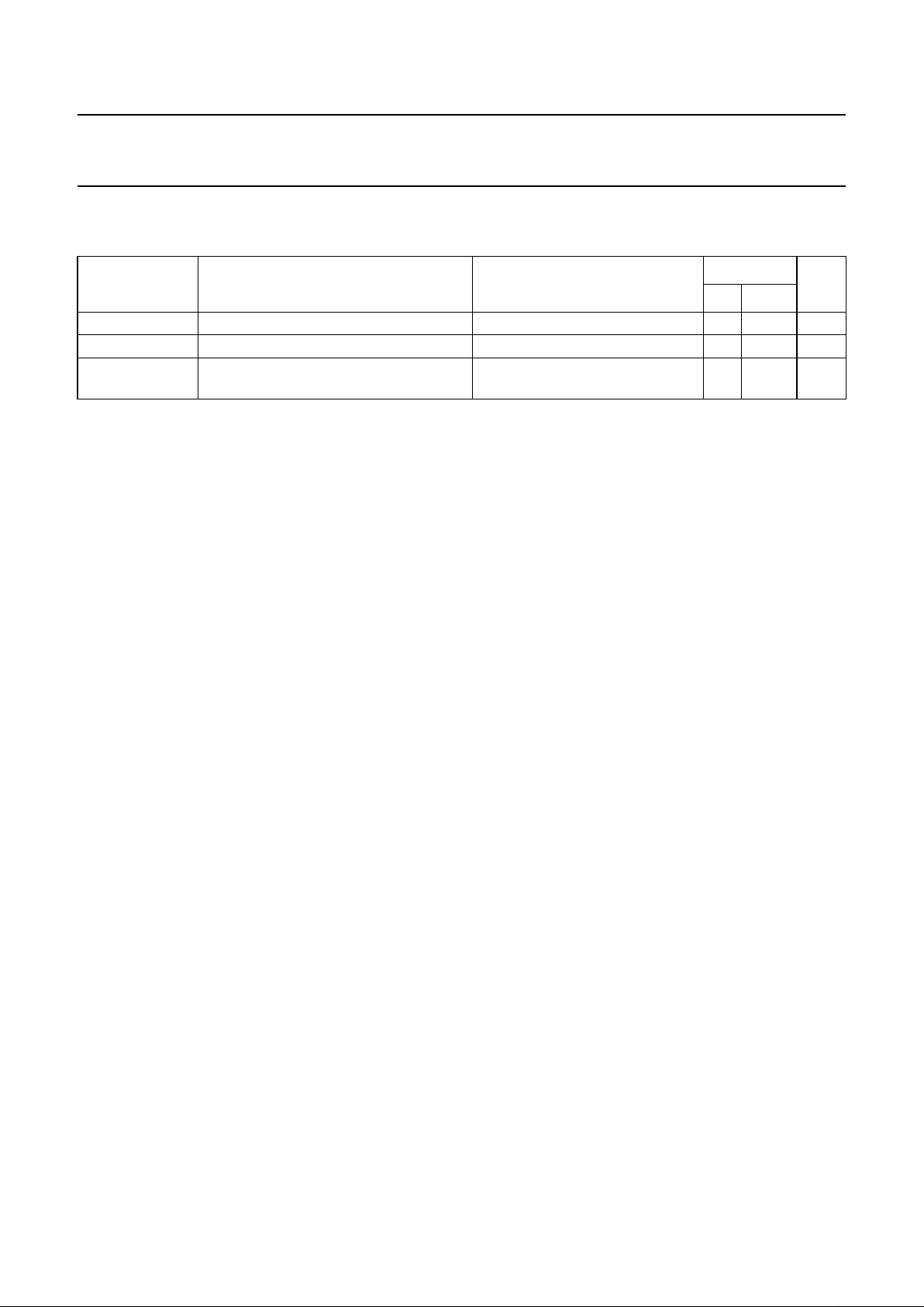
QUICK REFERENCE DATA
GND = 0 V; T
amb
=25°C
Notes
1. C
PD
is used to determine the dynamic power dissipation (PDin µW):
PD=CPD× V
CC
2
× fi+ ∑ (CL× V
CC
2
× fo) where:
fi= input frequency in MHz.
fo= output frequency in MHz.
CL= output load capacitance in pF.
VCC= supply voltage in V.
∑ (CL× V
CC
2
× fo) = sum of outputs.
2. Applies to the phase comparator section only (VCO disabled). For power dissipation of the VCO and demodulator
sections see Figs 22, 23 and 24.
ORDERING INFORMATION
See
“74HC/HCT/HCU/HCMOS Logic Package Information”
.
APPLICATIONS
• FM modulation and demodulation
• Frequency synthesis and multiplication
• Frequency discrimination
• Tone decoding
• Data synchronization and conditioning
• Voltage-to-frequency conversion
• Motor-speed control.
PACKAGE OUTLINES
See
“74HC/HCT/HCU/HCMOS Logic Package Outlines”
.
SYMBOL PARAMETER CONDITIONS
TYPICAL
UNIT
HC HCT
f
o
VCO centre frequency C1 = 40 pF; R1 = 3 kΩ;VCC= 5 V 19 19 MHz
C
I
input capacitance (pin 5) 3.5 3.5 pF
C
PD
power dissipation capacitance per
package
notes 1 and 2 24 24 pF
Page 5

1997 Nov 25 5
Philips Semiconductors Product specification
Phase-locked-loop with VCO 74HC/HCT4046A
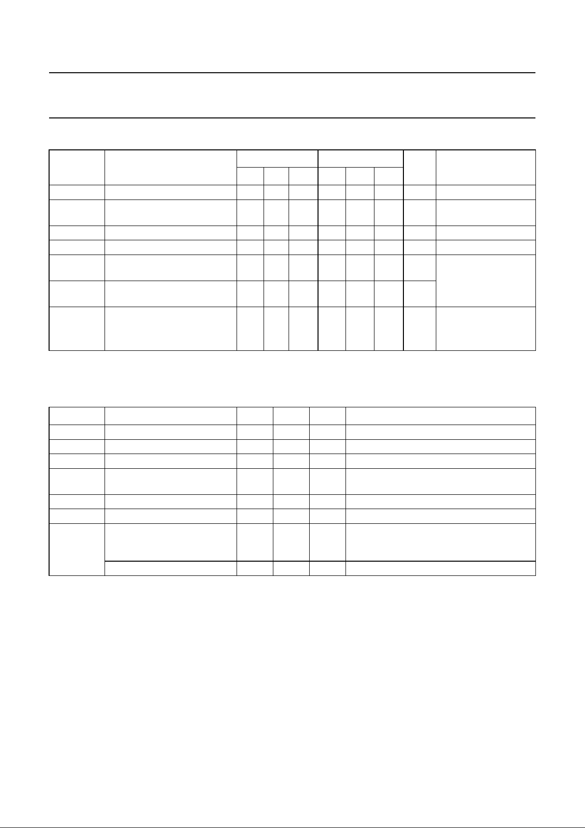
PIN DESCRIPTION
PIN NO. SYMBOL NAME AND FUNCTION
1 PCP
OUT
phase comparator pulse output
2 PC1
OUT
phase comparator 1 output
3 COMP
IN
comparator input
4 VCO
OUT
VCO output
5 INH inhibit input
6C1
A
capacitor C1 connection A
7C1
B
capacitor C1 connection B
8 GND ground (0 V)
9 VCO
IN
VCO input
10 DEM
OUT
demodulator output
11 R
1
resistor R1 connection
12 R
2
resistor R2 connection
13 PC2
OUT
phase comparator 2 output
14 SIG
IN
signal input
15 PC3
OUT
phase comparator 3 output
16 V
CC
positive supply voltage
Fig.1 Pin configuration. Fig.2 Logic symbol. Fig.3 IEC logic symbol.
Page 6

1997 Nov 25 6
Philips Semiconductors Product specification
Phase-locked-loop with VCO 74HC/HCT4046A
MGA847
PHASE
COMPARATOR
2
LOCK
DETECTOR
PC2
OUTLD13
1
identical to 4046A
C
LD
C
CLD
15
7046A
PHASE
COMPARATOR
2
PC2
OUT 13
PHASE
COMPARATOR
3
PC3
OUT 15
PHASE
COMPARATOR
1
PC1
OUT
2
PCP
OUT
1
SIG
IN
COMP
IN
V
CO OUT
C1AC1
B
DEM
OUTINH
VCO
IN
R
2
R
1
R2
12
11
314476
5109
(a)
(b)
C1
4046A
VCO
R
S
R1
R4
R3
C2
Fig.4 Functional diagram.
(a) (b)
Fig.5 Logic diagram.
Page 7

1997 Nov 25 7
Philips Semiconductors Product specification
Phase-locked-loop with VCO 74HC/HCT4046A
Fig.6 Phase comparator 1: average output voltage versus input phase difference.
V
DEMOUT=VPC2OUT
=
φ
DEMOUT
=(φ
SIGIN−φCOMPIN
).
V
CC
π
---------- -
φ
SIGINφCOMPIN
–()
Fig.7 Typical waveforms for PLL using phase comparator 1, loop locked at fo.
Fig.8 Phase comparator 2: average output voltage versus input phase difference.
V
DEMOUT=VPC2OUT
=
φ
DEMOUT
=(φ
SIGIN
−φC
OMPIN
).
V
CC
4π
---------- -
φ
SIGINφCOMPIN
–()
Page 8

1997 Nov 25 8
Philips Semiconductors Product specification
Phase-locked-loop with VCO 74HC/HCT4046A
Fig.9 Typical waveforms for PLL using phase comparator 2, loop locked at fo.
Fig.10 Phase comparator 3: average output voltage versus input phase difference:
V
DEMOUT=VPC3OUT
=
φ
DEMOUT
=(φ
SIGIN−φCOMPIN
).
V
CC
2π
---------- -
φ
SIGINφCOMPIN
–()
Fig.11 Typical waveforms for PLL using phase comparator 3, loop locked at fo.
Page 9
1997 Nov 25 9
Philips Semiconductors Product specification
Phase-locked-loop with VCO 74HC/HCT4046A
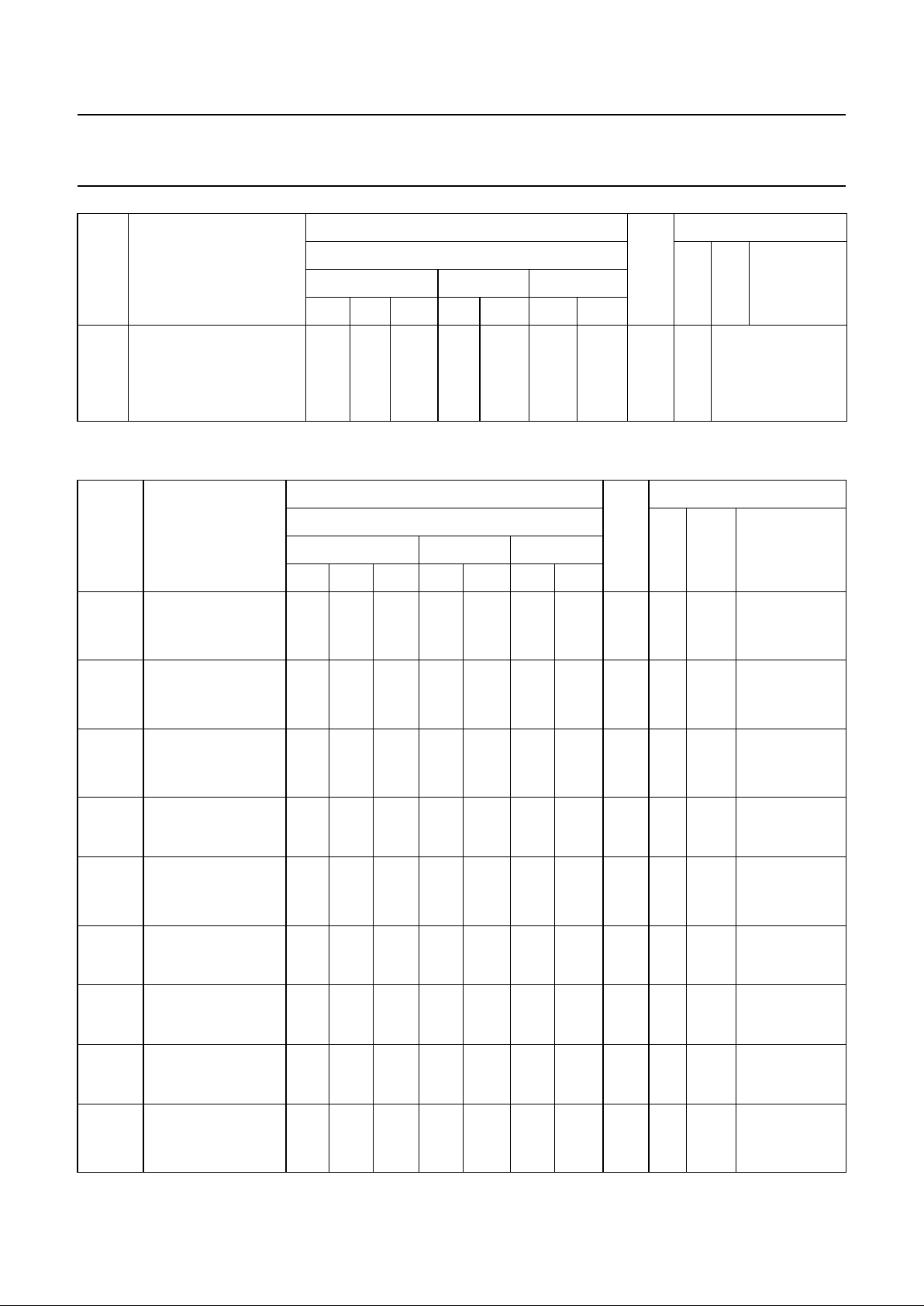
RECOMMENDED OPERATING CONDITIONS FOR 74HC/HCT
RATINGS
Limiting values in accordance with the Absolute Maximum System (IEC 134)
Voltages are referenced to GND (ground = 0 V)
SYMBOL PARAMETER
74HC 74HCT
UNIT CONDITIONS
min. typ. max. min. typ. max.
V
CC
DC supply voltage 3.0 5.0 6.0 4.5 5.0 5.5 V
V
CC
DC supply voltage if VCO
section is not used
2.0 5.0 6.0 4.5 5.0 5.5 V
V
I
DC input voltage range 0 V
CC
0V
CC
V
V
O
DC output voltage range 0 V
CC
0V
CC
V
T
amb
operating ambient
temperature range
−40 +85 −40 +85 °C see DC and AC
CHARACTERISTICS
T
amb
operating ambient
temperature range
−40 +125 −40 +125 °C
t
r,tf
input rise and fall times (pin 5) 6.0 1000 6.0 500 ns VCC= 2.0 V
6.0 500 6.0 500 ns V
CC
= 4.5 V
6.0 400 6.0 500 ns V
CC
= 6.0 V
SYMBOL PARAMETER MIN. MAX. UNIT CONDITIONS
V
CC
DC supply voltage −0.5 +7 V
±I
IK
DC input diode current 20 mA for VI<−0.5 V or VI> VCC+ 0.5 V
±I
OK
DC output diode current 20 mA for VO<−0.5 V or VO> VCC+ 0.5 V
±I
O
DC output source or sink
current
25 mA for −0.5 V < VO< VCC+ 0.5 V
±I
CC
; ±I
GND
DC VCCor GND current 50 mA
T
stg
storage temperature range −65 +150 °C
P
tot
power dissipation per package
plastic DIL 750 mW
for temperature range: − 40 to +125 °C
74HC/HCT
above + 70 °C: derate linearly with 12 mW/K
plastic mini-pack (SO) 500 mW above + 70 °C: derate linearly with 8 mW/K
Page 10

1997 Nov 25 10
Philips Semiconductors Product specification
Phase-locked-loop with VCO 74HC/HCT4046A
DC CHARACTERISTICS FOR 74HC
Quiescent supply current
Voltages are referenced to GND (ground = 0 V)
Phase comparator section
Voltages are referenced to GND (ground = 0 V)
SYMBOL PARAMETER
T
amb
(°C)
UNIT
TEST CONDITIONS
74HC V
CC
(V)
OTHER
+25 −40 to +85 −40 to +125
min. typ. max. min. max. min. max.
I
CC
quiescent supply
current (VCO
disabled)
8.0 80.0 160.0 µA 6.0
pins 3, 5, and 14 at VCC;
pin 9 at GND; I
I
at pins
3 and 14 to be excluded
SYMBOL
PARAMETER
T
amb
(°C)
UNIT
TEST CONDITIONS
74HC V
CC
(V)
V
I
OTHER
+25 −40 to +85 −40 to +125
min. typ. max. min. max. min. max.
V
IH
DC coupled
HIGH level input voltage
SIGIN, COMP
IN
1.5 1.2 1.5 1.5 V 2.0
3.15 2.4 3.15 3.15 4.5
4.2 3.2 4.2 4.2 6.0
V
IL
DC coupled
LOW level input voltage
SIGIN, COMP
IN
0.8 0.5 0.5 0.5 V 2.0
2.1 1.35 1.35 1.35 4.5
2.8 1.8 1.8 1.8 6.0
V
OH
HIGH level output voltage
PCP
OUT
,PC
nOUT
1.9 2.0 1.9 1.9 V 2.0 V
IH
or
V
IL
−IO=20µA
4.4 4.5 4.4 4.4 4.5 −I
O
=20µA
5.9 6.0 5.9 5.9 6.0 −I
O
=20µA
V
OH
HIGH level output voltage
PCP
OUT
,PC
nOUT
3.98 4.32 3.84 3.7 V 4.5 V
IH
or
V
IL
−IO= 4.0 mA
5.48 5.81 5.34 5.2 6.0 −I
O
= 5.2 mA
V
OL
LOW level output voltage
PCP
OUT
,PC
nOUT
0 0.1 0.1 0.1 V 2.0 V
IH
or
V
IL
IO=20µA
0 0.1 0.1 0.1 4.5 I
O
=20µA
0 0.1 0.1 0.1 6.0 I
O
=20µA
V
OL
LOW level output voltage
PCP
OUT
,PC
nOUT
0.15 0.26 0.33 0.4 V 4.5 V
IH
or
V
IL
IO= 4.0 mA
0.16 0.26 0.33 0.4 6.0 I
O
= 5.2 mA
±I
I
input leakage current
SIGIN, COMP
IN
3.0 4.0 5.0 µA 2.0 V
CC
or
GND
7.0 9.0 11.0 3.0
18.0 23.0 27.0 4.5
30.0 38.0 45.0 6.0
±I
OZ
3-state
OFF-state current
PC2
OUT
0.5 5.0 10.0 µA 6.0 V
IH
or
V
IL
VO=VCCor
GND
Page 11
1997 Nov 25 11
Philips Semiconductors Product specification
Phase-locked-loop with VCO 74HC/HCT4046A
VCO section
Voltages are referenced to GND (ground = 0 V)
R
I
input resistance
SIGIN, COMP
IN
800 kΩ 3.0 V
I
at self-bias
operating point;
∆ V
I
= 0.5 V;
see Figs 12, 13
and 14
250 kΩ 4.5
150 kΩ 6.0
SYMBOL
PARAMETER
T
amb
(°C)
UNIT
TEST CONDITIONS
74HC V
CC
(V)
V
I
OTHER
+25 −40 to +85 −40 to +125
min. typ. max. min. max. min. max.
V
IH
HIGH level
input voltage
INH
2.1 1.7 2.1 2.1 V 3.0
3.15 2.4 3.15 3.15 4.5
4.2 3.2 4.2 4.2 6.0
V
IL
LOW level
input voltage
INH
1.3 0.9 0.9 0.9 V 3.0
2.1 1.35 1.35 1.35 4.5
2.8 1.8 1.8 1.8 6.0
V
OH
HIGH level
output voltage
VCO
OUT
2.9 3.0 2.9 2.9 V 3.0 V
IH
or
V
IL
−IO=20µA
4.4 4.5 4.4 4.4 4.5 −I
O
=20µA
5.9 6.0 5.9 5.9 6.0 −I
O
=20µA
V
OH
HIGH level
output voltage
VCO
OUT
3.98 4.32 3.84 3.7 V 4.5 V
IH
or
V
IL
−IO= 4.0 mA
5.48 5.81 5.34 5.2 6.0 −I
O
= 5.2 mA
V
OL
LOW level
output voltage
VCO
OUT
0 0.1 0.1 0.1 V 3.0 V
IH
or
V
IL
IO=20µA
0 0.1 0.1 0.1 4.5 I
O
=20µA
0 0.1 0.1 0.1 6.0 I
O
=20µA
V
OL
LOW level
output voltage
VCO
OUT
0.15 0.26 0.33 0.4 V 4.5 V
IH
or
V
IL
IO= 4.0 mA
0.16 0.26 0.33 0.4 6.0 I
O
= 5.2 mA
V
OL
LOW level output
voltage C1A,C1
B
0.40 0.47 0.54 V 4.5 V
IH
or
V
IL
IO= 4.0 mA
0.40 0.47 0.54 6.0 I
O
= 5.2 mA
±I
I
input leakage
current
INH, VCO
IN
0.1 1.0 1.0 µA 6.0 V
CC
or
GND
R1 resistor range 3.0 300 kΩ 3.0 note 1
3.0 300 4.5
3.0 300 6.0
SYMBOL
PARAMETER
T
amb
(°C)
UNIT
TEST CONDITIONS
74HC V
CC
(V)
V
I
OTHER
+25 −40 to +85 −40 to +125
min. typ. max. min. max. min. max.
Page 12

1997 Nov 25 12
Philips Semiconductors Product specification
Phase-locked-loop with VCO 74HC/HCT4046A
Note
1. The parallel value of R1 and R2 should be more than 2.7 kΩ. Optimum performance is achieved when R1 and/ or
R2 are/is > 10 kΩ.
Demodulator section
Voltages are referenced to GND (ground = 0 V)
R
2
resistor range 3.0 300 kΩ 3.0 note 1
3.0 300 4.5
3.0 300 6.0
C1 capacitor range 40 no
limit
pF 3.0
40 4.5
40 6.0
V
VCOIN
operating voltage
range at VCO
IN
1.1 1.9 V 3.0 over the range
specified for
R1; for linearity
see Figs 20
and 21
1.1 3.4 4.5
1.1 4.9 6.0
SYMBOL PARAMETER
T
amb
(°C)
UNIT
TEST CONDITIONS
74HC
V
CC
V
OTHER
+25 −40 to+85 −40 to +125
min. typ. max. min. max. min. max.
R
S
resistor range 50 300 kΩ 3.0 at RS> 300 kΩ
the leakage current can
influence V
DEMOUT
50 300 4.5
50 300 6.0
V
OFF
offset voltage
VCOINto V
DEMOUT
±30 mV 3.0 VI=V
VCOIN
= 1/2 VCC;
values taken over
RSrange; see Fig.15
±20 4.5
±10 6.0
R
D
dynamic output
resistance at DEM
OUT
25 Ω 3.0 V
DEMOUT
= 1/2 V
CC
25 4.5
25 6.0
SYMBOL
PARAMETER
T
amb
(°C)
UNIT
TEST CONDITIONS
74HC V
CC
(V)
V
I
OTHER
+25 −40 to +85 −40 to +125
min. typ. max. min. max. min. max.
Page 13

1997 Nov 25 13
Philips Semiconductors Product specification
Phase-locked-loop with VCO 74HC/HCT4046A
AC CHARACTERISTICS FOR 74HC
Phase comparator section
GND = 0 V; t
r=tf
= 6 ns; CL= 50 pF
SYMBOL PARAMETER
T
amb
(°C)
UNIT
TEST
CONDITIONS
74HC
V
CC
(V)
OTHER
+25 −40 to +85 −40 to +125
min. typ. max. min. max. min. max.
t
PHL
/
t
PLH
propagation delay
SIGIN, COMP
IN
to PC1
OUT
63 200 250 300 ns 2.0 Fig.16
23 40 50 60 4.5
18 34 43 51 6.0
t
PHL
/
t
PLH
propagation delay
SIGIN, COMP
IN
to PCP
OUT
96 340 425 510 ns 2.0 Fig.16
35 68 85 102 4.5
28 58 72 87 6.0
t
PHL
/
t
PLH
propagation delay
SIGIN, COMP
IN
to PC3
OUT
77 270 340 405 ns 2.0 Fig.16
28 54 68 81 4.5
22 46 58 69 6.0
t
PZH
/
t
PZL
3-state output enable
time SIGIN, COMP
IN
to PC2
OUT
83 280 350 420 ns 2.0 Fig.17
30 56 70 84 4.5
24 48 60 71 6.0
t
PHZ
/
t
PLZ
3-state output disable
time SIGIN, COMP
IN
to PC2
OUT
99 325 405 490 ns 2.0 Fig.17
36 65 81 98 4.5
29 55 69 83 6.0
t
THL
/
t
TLH
output transition time 19 75 95 110 ns 2.0 Fig.16
7 15 19 22 4.5
6 13 16 19 6.0
V
I(p-p)
AC coupled input sensitivity
(peak-to-peak value) at
SIGINor COMP
IN
9 mV 2.0 fi= 1 MHz
1 1 3.0
15 4.5
33 6.0
Page 14

1997 Nov 25 14
Philips Semiconductors Product specification
Phase-locked-loop with VCO 74HC/HCT4046A
VCO section
GND = 0 V; t
r=tf
= 6 ns; CL= 50 pF
DC CHARACTERISTICS FOR 74HCT
Quiescent supply current
Voltages are referenced to GND (ground = 0 V)
Note
1. The value of additional quiescent supply current (∆I
CC
) for a unit load of 1 is given above.
To determine ∆ICCper input, multiply this value by the unit load coefficient shown in the table below.
SYMBOL PARAMETER
T
amb
(°C)
UNIT
TEST CONDITIONS
74HC
V
CC
(V)
OTHER
+25 −40 to +85 −40 to +125
min. typ. max. typ. max. min. max.
∆f/T frequency stability
with temperature
change
0.20 %/K 3.0
VI=V
VCOIN
= 1/2 VCC;
R1 = 100 kΩ;R2=∞;
C1 = 100 pF; see Fig.18
0.15 4.5
0.14 6.0
f
o
VCO centre
frequency (duty
factor = 50%)
7.0 10.0 MHz 3.0 V
VCOIN
= 1/2 VCC;
R1 = 3 kΩ;R2=∞;
C1 = 40 pF; see Fig.19
11.0 17.0 4.5
13.0 21.0 6.0
∆f
VCO
VCO frequency
linearity
1.0 % 3.0 R1 = 100 kΩ;R2=∞;
C1 = 100 pF;
see Figs 20 and 21
0.4 4.5
0.3 6.0
δ
VCO
duty factor at
VCO
OUT
50 % 3.0
50 4.5
50 6.0
SYMBOL PARAMETER
T
amb
(°C)
UNIT
TEST CONDITIONS
74HCT
V
CC
(V)
OTHER
+25 −40 to +85 −40 to +125
min. typ. max. min. max. min. max.
I
CC
quiescent supply
current
(VCO disabled)
8.0 80.0 160.0 µA 6.0 pins 3, 5 and 14
at VCC; pin 9 at
GND; IIat
pins 3 and 14 to
be excluded
∆I
CC
additional quiescent
supply current per
input pin for unit load
coefficient is 1 (note 1)
VI=VCC− 2.1 V
100 360 450 490 µA 4.5
to
5.5
pins 3 and 14
at VCC;
pin 9 at GND;
IIat pins 3 and 14
to be excluded
INPUT UNIT LOAD COEFFICIENT
INH 1.00
Page 15

1997 Nov 25 15
Philips Semiconductors Product specification
Phase-locked-loop with VCO 74HC/HCT4046A
DC CHARACTERISTICS FOR 74HCT
Phase comparator section
Voltages are referenced to GND (ground=0V)
SYMBOL PARAMETER
T
amb
(°C)
UNIT
TEST CONDITIONS
74HCT
V
CC
(V)
VIOTHER
+25 −40 to +85 −40 to +125
min typ. max min max min. max.
V
IH
DC coupled
HIGH level input
voltage SIGIN, COMP
IN
3.15 2.4 V 4.5
V
IL
DC coupled
LOW level input
voltage
SIGIN, COMP
IN
2.1 1.35 V 4.5
V
OH
HIGH level output
voltage PCP
OUT
,
PC
nOUT
4.4 4.5 4.4 4.4 V 4.5 V
IH
or
V
IL
−IO=20µA
V
OH
HIGH level output
voltage PCP
OUT
,
PC
nOUT
3.98 4.32 3.84 3.7 V 4.5 V
IH
or
V
IL
−IO= 4.0 mA
V
OL
LOW level output
voltage
PCP
OUT
,PC
nOUT
0 0.1 0.1 0.1 V 4.5 V
IH
or
V
IL
IO=20µA
V
OL
LOW level output
voltage
PCP
OUT
,PC
nOUT
0.15 0.26 0.33 0.4 V 4.5 V
IH
or
V
IL
IO= 4.0 mA
±I
I
input leakage current
SIGIN, COMP
IN
30 38 45 µA 5.5 V
CC
or
GN
D
±I
OZ
3-state OFF-state
current PC2
OUT
0.5 5.0 10.0 µA 5.5 V
IH
or
V
IL
VO=VCCor
GND
R
I
input resistance
SIGIN, COMP
in
250 kΩ 4.5 V
I
at self-bias
operating
point;
∆ V
I
= 0.5 V;
see Figs 12
, 13 and
14
Page 16

1997 Nov 25 16
Philips Semiconductors Product specification
Phase-locked-loop with VCO 74HC/HCT4046A
DC CHARACTERISTICS FOR 74HCT
VCO section
Voltages are referenced to GND (ground = 0 V)
Note
1. The parallel value of R1 and R2 should be more than 2.7 kΩ. Optimum performance is achieved when R1 and/or R2
are/is > 10 kΩ.
SYMBOL PARAMETER
T
amb
(°C)
UNIT
TEST CONDITIONS
74HCT
V
CC
(V)
VIOTHER
+25 −40 to +85 −40 to +125
min typ. max min max min. max.
V
IH
HIGH level
input voltage INH
2.0 1.6 2.0 2.0 V 4.5
to
5.5
V
IL
LOW level
input voltage INH
1.2 0.8 0.8 0.8 V 4.5
to
5.5
V
OH
HIGH level output
voltage VCO
OUT
4.4 4.5 4.4 4.4 V 4.5 V
IH
or
V
IL
−IO=20µA
V
OH
HIGH level output
voltage VCO
OUT
3.98 4.32 3.84 3.7 V 4.5 V
IH
or
V
IL
−IO= 4.0 mA
V
OL
LOW level output
voltage VCO
OUT
0 0.1 0.1 0.1 V 4.5 V
IH
or
V
IL
IO=20µA
V
OL
LOW level output
voltage VCO
OUT
0.15 0.26 0.33 0.4 V 4.5 V
IH
or
V
IL
IO= 4.0 mA
V
OL
LOW level output
voltage C1A,C1
B
(test purposes only)
0.40 0.47 0.54 V 4.5 V
IH
or
V
IL
IO= 4.0 mA
±I
I
input leakage
current
INH, VCO
IN
0.1 1.0 1.0 µA 5.5 V
CC
or
GND
R1 resistor range 3.0 300 kΩ 4.5 note 1
R
2
resistor range 3.0 300 kΩ 4.5 note 1
C1 capacitor range 40 no
limit
pF 4.5
V
VCOIN
operating voltage
range at VCO
IN
1.1 3.4 V 4.5 over the
range
specified for
R1; for
linearity see
Figs 20
and 21
Page 17

1997 Nov 25 17
Philips Semiconductors Product specification
Phase-locked-loop with VCO 74HC/HCT4046A
DC CHARACTERISTICS FOR 74HCT
Demodulator section
Voltages are referenced to GND (ground = 0 V)
AC CHARACTERISTICS FOR 74HCT
Phase comparator section
GND = 0 V; t
r=tf
= 6 ns; CL= 50 pF
SYMBOL PARAMETER
T
amb
(°C)
UNIT
TEST CONDITIONS
74HCT
V
CC
(V)
OTHER
+25 −40 to +85 −40 to +125
min. typ. max. min. max. min. max.
R
S
resistor range 50 300 kΩ 4.5 at R
S
> 300 kΩ
the leakage current can
influence V
DEMOUT
V
OFF
offset voltage
VCOINto
V
DEMOUT
±20 mV 4.5 V
I=VVCOIN
= 1/2 VCC;
values taken over
R
S
range; see Fig.15
R
D
dynamic output
resistance at
DEM
OUT
25 Ω 4.5 V
DEMOUT
= 1/2 V
CC
SYMBOL PARAMETER
T
amb
(°C)
UNIT
TEST CONDITIONS
74HCT
V
CC
(V)
OTHER
+25 −40 to +85 −40 to +125
min. typ. max. min. max. min. max.
t
PHL
/
t
PLH
propagation delay
SIGIN, COMP
IN
to PC1
OUT
23 40 50 60 ns 4.5 Fig.16
t
PHL
/
t
PLH
propagation delay
SIGIN, COMP
IN
to PCP
OUT
35 68 85 102 ns 4.5 Fig.16
t
PHL
/
t
PLH
propagation delay
SIGIN, COMP
IN
to PC3
OUT
28 54 68 81 ns 4.5 Fig.16
t
PZH
/
t
PZL
3-state output enable
time SIGIN, COMP
IN
to PC2
OUT
30 56 70 84 ns 4.5 Fig.17
Page 18

1997 Nov 25 18
Philips Semiconductors Product specification
Phase-locked-loop with VCO 74HC/HCT4046A
VCO section
GND = 0 V; t
r=tf
= 6 ns; CL= 50 pF
t
PHZ
/
t
PLZ
3-state output disable
time SIGIN, COMP
IN
to PC2
OUT
36 65 81 98 ns 4.5 Fig.17
t
THL
/
t
TLH
output transition time 7 15 19 22 ns 4.5 Fig.16
V
I (p-p)
AC coupled input
sensitivity
(peak-to-peak value)
at
SIGINor COMP
IN
15 mV 4.5 fi= 1 MHz
SYMBOL PARAMETER
T
amb
(°C)
UNIT
TEST CONDITIONS
74HCT
V
CC
(V)
OTHER
+25 −40 to +85 −40 to +125
min. typ. max min. max min. max.
∆f/T frequency stability
with temperature
change
0.15 %/K 4.5
VI=V
VCOIN
withi
n recommended
range;
R1 = 100 kΩ;
R2 = ∞;
C1 = 100 pF;
see Fig.18b
f
o
VCO centre frequency
(duty factor = 50%)
11.0 17.0 MHz 4.5 V
VCOIN
= 1/2 V
CC
;
R1 = 3 kΩ;
R2 = ∞;
C1 = 40 pF;
see Fig.19
∆f
VCO
VCO frequency
linearity
0.4 % 4.5 R1 = 100 kΩ;
R2 = ∞;
C1 = 100 pF;
see Figs 20
and 21
δ
VCO
duty factor at VCO
OUT
50 % 4.5
SYMBOL PARAMETER
T
amb
(°C)
UNIT
TEST CONDITIONS
74HCT
V
CC
(V)
OTHER
+25 −40 to +85 −40 to +125
min. typ. max. min. max. min. max.
Page 19

1997 Nov 25 19
Philips Semiconductors Product specification
Phase-locked-loop with VCO 74HC/HCT4046A
FIGURE REFERENCES FOR DC CHARACTERISTICS
Fig.12 Typical input resistance curve at SIGIN,
COMPIN.
Fig.13 Input resistance at SIGIN, COMPINwith
∆VI= 0.5 V at self-bias point.
Fig.14 Input current at SIGIN, COMPINwith
∆VI= 0.5 V at self-bias point.
Fig.15 Offset voltage at demodulator output as a
function of VCOINand RS.
RS=50kΩ
----R
S
= 300 kΩ
Page 20

1997 Nov 25 20
Philips Semiconductors Product specification
Phase-locked-loop with VCO 74HC/HCT4046A
AC WAVEFORMS
Fig.16 Waveforms showing input (SIGIN, COMPIN) to output (PCP
OUT
, PC1
OUT
, PC3
OUT
) propagation delays
and the output transition times.
(1) HC : VM= 50%; VI= GND to V
CC
Fig.17 Waveforms showing the 3-state enable and disable times for PC2
OUT
.
(1) HC : VM= 50%; VI= GND to V
CC
Page 21

1997 Nov 25 21
Philips Semiconductors Product specification
Phase-locked-loop with VCO 74HC/HCT4046A
Fig.18 Frequency stability of the VCO as a function of ambient temperature with supply voltage as a parameter.
without offset (R2 = ∞): (a) R1= 3 kΩ; (b) R1 = 10 kΩ; (c) R1 = 300 kΩ.
−−− with offset (R1 = ∞): (a) R2 = 3 kΩ; (b) R2 = 10 kΩ; (c) R2 = 300 kΩ.
In (b), the frequency stability for R1 = R2 = 10 kΩ at 5 V is also given (curve A). This curve is set by the total VCO bias current, and is
not simply the addition of the two 10 kΩ stability curves. C1 = 100 pF; V
VCO IN
= 0.5 VCC.
To obtain optimum temperature stability, C1 must be as small as possible but larger than 100 pF.
ook, halfpage
MSB710
T
amb
(oC)
0
150100500−50
−25
−20
−15
−10
−5
5
10
15
20
25
∆
f
(%)
5 V
6 V
3 V
4.5 V
5 V
6 V
V =
CC
3 V
(a)
handbook, halfpage
MSB711
T ( C)
amb
0
f
(%)
o
15010050050
25
20
15
10
5
5
10
15
20
25
∆
5 V
6 V
3 V
5 V
6 V
V =
CC
3 V
(b)
A
handbook, halfpage
MSB712
T ( C)
amb
0
f
(%)
o
15010050050
25
20
15
10
5
5
10
15
20
25
∆
5 V
6 V
(c)
V =
CC
3 V
3 V
6 V
5 V
Page 22

1997 Nov 25 22
Philips Semiconductors Product specification
Phase-locked-loop with VCO 74HC/HCT4046A
Fig.18 Continued.
(d) R2=3kΩ
R
1
=∞
(e) R2=10kΩ
R
1
=∞
(f) R2= 300 kΩ
R
1
= ∞
To obtain optimum temperature stability, C1 must be as small as possible but larger than 100 pF.
Page 23

1997 Nov 25 23
Philips Semiconductors Product specification
Phase-locked-loop with VCO 74HC/HCT4046A
Fig.19 Graphs showing VCO frequency (f
VCO
) as a function of the VCO input voltage (V
VCOIN
).
(a) R1=3kΩ;
C
1
= 40 pF
(c) R1= 300 kΩ;
C
1
=40pF
(d) R1= 300 kΩ;
C
1
= 100 nF
(b) R1=3kΩ;
C
1
= 100 nF
To obtain optimum temperature stability, C1 must be as small as possible but larger than 100 pF.
Page 24

1997 Nov 25 24
Philips Semiconductors Product specification
Phase-locked-loop with VCO 74HC/HCT4046A
Fig.20 Definition of VCO frequency linearity:
∆V = 0.5 V over the VCCrange:
for VCO linearity
f‘
0
f1f2+
2
-------------- -
=
linearity
f‘
0f0
–
f‘
0
----------------
100%×=
Fig.21 Frequency linearity as a function of R1, C1
and VCC: R2 = ∞ and ∆V = 0.5 V.
Fig.22 Power dissipation
versus the value of R1:
CL= 50 pF;
R2 = ∞;
V
VCOIN
= 1/2 VCC;
T
amb
=25°C.
C1 = 40 pF
- - - -C1 = 1 µF
Fig.23 Power dissipation
versus the value of R2:
CL= 50 pF;
R1 = ∞;
V
VCOIN
=GND=0V;
T
amb
=25°C.
C1 = 40 pF
- - - - C1 = 1 µF
Fig.24 Typical dc power
dissipation of
demodulator sections
as a function of RS:
R1=R2=∞;
T
amb
=25°C;
V
VCOIN
= 1/2 VCC.
Page 25

1997 Nov 25 25
Philips Semiconductors Product specification
Phase-locked-loop with VCO 74HC/HCT4046A
APPLICATION INFORMATION
This information is a guide for the approximation of values of external components to be used with the 74HC/HCT4046A
in a phase-lock-loop system.
References should be made to Figs 29, 30 and 31 as indicated in the table.
Values of the selected components should be within the following ranges:
R1 between 3 kΩ and 300 kΩ;
R2 between 3 kΩ and 300 kΩ;
R1 + R2 parallel value > 2.7 kΩ;
C1 greater than 40 pF.
SUBJECT
PHASE
COMPARATOR
DESIGN CONSIDERATIONS
VCO frequency characteristic
VCO frequency
without extra
offset
PC1, PC2 or PC3 With R2 = ∞ and R1 within the range 3 kΩ<R1 < 300 kΩ, the
characteristics of the VCO operation will be as shown in Fig.25.
(Due to R1, C1 time constant a small offset remains when R2 = ∞.).
Fig.25 Frequency characteristic of VCO operating without offset:
f
0
= centre frequency; 2fL= frequency lock range.
Selection of R1 and C1
PC1 Given fo, determine the values of R1 and C1 using Fig.29.
PC2 or PC3 Given f
max
and fo, determine the values of R1 and C1 using Fig.29, use
Fig.31 to obtain 2fLand then use this to calculate f
min
.
Page 26

1997 Nov 25 26
Philips Semiconductors Product specification
Phase-locked-loop with VCO 74HC/HCT4046A
VCO frequency characteristic
VCO frequency
with extra
offset
PC1, PC2 or PC3 With R1 and R2 within the ranges 3 kΩ<R1 < 300 kΩ,
3kΩ<R2 < 300 kΩ, the characteristics of the VCO operation will be as
shown in Fig.26.
Fig.26 Frequency characteristic of VCO operating with offset:
f
o
= centre frequency; 2fL= frequency lock range.
Selection of R1, R2 and C1
PC1, PC2 or PC3 Given foand fL, determine the value of product R1C1 by using Fig.31.
Calculate f
off
from the equation f
off=fo
1.6fL.
Obtain the values of C1 and R2 by using Fig.30.
Calculate the value of R1 from the value of C1 and the product R1C1.
PLL conditions
with no signal at
the SIG
IN
input
PC1 VCO adjusts to fowith φ
DEMOUT
=90°and V
VCOIN
= 1/2 VCC(see Fig.6).
PC2 VCO adjusts to f
o
with φ
DEMOUT
= −360° and V
VCOIN
= min. (see Fig.8).
PC3 VCO adjusts to f
o
with φ
DEMOUT
= −360° and V
VCOIN
= min. (see Fig.10).
SUBJECT
PHASE
COMP ARATOR
DESIGN CONSIDERATIONS
Page 27

1997 Nov 25 27
Philips Semiconductors Product specification
Phase-locked-loop with VCO 74HC/HCT4046A
PLL frequency
capture range
PC1, PC2 or PC3 Loop filter component selection
(a) τ = R3 x C2 (b) amplitude characteristic (c) pole-zero diagram
A small capture range (2f
c
) is obtained if
Fig. 27 Simple loop filter for PLL without offset; R3 ≥ 500 Ω.
(a) τ1 = R3 x C2; (b) amplitude characteristic (c) pole-zero diagram
τ2 = R4 x C2;
τ3 = (R3 + R4) x C2
Fig.28 Simple loop filter for PLL with offset; R3 + R4 ≥ 500 Ω.
PLL locks on
harmonics at
centre frequency
PC1 or PC3 yes
PC2 no
noise rejection at
signal input
PC1 high
PC2 or PC3 low
AC ripple content
when PLL is
locked
PC1 f
r
=2fi, large ripple content at φ
DEMOUT
=90°
PC2 f
r=fi
, small ripple content at φ
DEMOUT
=0°
PC3 f
r=fi
, large ripple content at φ
DEMOUT
= 180°
SUBJECT
PHASE
COMPARATOR
DESIGN CONSIDERATIONS
2f
c
1
π
-- -
2 π f
L
τ⁄≈
Page 28

1997 Nov 25 28
Philips Semiconductors Product specification
Phase-locked-loop with VCO 74HC/HCT4046A
Fig.29 Typical value of VCO centre frequency (fo) as a function of C1: R2 = ∞; V
VCOIN
= 1/2 VCC; INH = GND;
T
amb
=25°C.
To obtain optimum VCO performance, C1 must be as small as possible but larger than 100 pF.
Interpolation for various values of R1 can be easily calculated because a constant R1C1 product will produce almost the same VCO output frequency.
Page 29

1997 Nov 25 29
Philips Semiconductors Product specification
Phase-locked-loop with VCO 74HC/HCT4046A
Fig.30 Typical value of frequency offset as a function of C1: R1 = ∞;V
VCOIN
= 1/2 VCC; INH = GND; T
amb
=25°C.
To obtain optimum VCO performance, C1 must be as small as possible but larger than 100 pF.
Interpolation for various values of R2 can be easily calculated because a constant R2C1 product will produce almost the same VCO output frequency.
Page 30

1997 Nov 25 30
Philips Semiconductors Product specification
Phase-locked-loop with VCO 74HC/HCT4046A
Fig.31 Typical frequency lock range (2fL) versus the product R1C1: V
VCOIN
range = 0.9 to (VCC− 0.9) V;
R2 = ∞; VCO gain:
K
V
2f
L
V
VCOIN
range
-------------------------------------
2 π rsV⁄⁄()
˙
.=
Page 31

1997 Nov 25 31
Philips Semiconductors Product specification
Phase-locked-loop with VCO 74HC/HCT4046A
PLL design example
The frequency synthesizer, used in
the design example shown in Fig.32,
has the following parameters:
Output frequency: 2 MHz to 3 MHz
frequency steps : 100 kHz
settling time : 1 ms
overshoot : < 20%
The open-loop gain is
H (s) x G (s) = Kp× Kf× Ko× Kn.
Where:
K
p
= phase comparator gain
Kf= low-pass filter transfer gain
Ko=Kv/s VCO gain
Kn= 1/n divider ratio
The programmable counter ratio
K
n
can be found as follows:
The VCO is set by the values of R1,
R2 and C1, R2 = 10 kΩ (adjustable).
The values can be determined using
the information in the section
“DESIGN CONSIDERATIONS”.
With f
o
= 2.5 MHz and fL= 500 kHz
this gives the following values
(VCC= 5.0 V):
R1 = 10 kΩ
R2 = 10 kΩ
C1 = 500 pF
N
min.
f
out
f
step
-----------
2MHz
100 kHz
----------------------
20== =
N
max.
f
out
f
step
-----------
3MHz
100 kHz
----------------------
30== =
The VCO gain is:
The gain of the phase
comparator is:
The transfer gain of the filter is
given by:
Where:
The characteristics equation is:
1+H(s)×G (s) = 0.
This results in:
The natural frequency ω
n
is
defined as follows:
K
v
2fL2 π××
0.9 V
CC
0.9–()–
---------------------------------------------- -
˙
==
1MHz
3.2
-----------------
2 π 210
6
×≈× r/s/V=
K
p
V
CC
4 π×
------------
0.4 V/r.==
K
f
1τ
2
s+
1τ
1
τ
2
+()s+
------------------------------------ -
.=
τ
1
R3C2 and τ2R4C2.==
s
2
1KpKvKnτ
2
×××+
τ
1τ2
+()
-----------------------------------------------------
s++
K
pKvKn
××
τ
1τ2
+()
--------------------------------
0.=
ω
n
KpKvKn××
τ
1τ2
+()
-------------------------------- .=
and the damping value ζ is defined as
follows:
In Fig.33 the output frequency response to
a step of input frequency is shown.
The overshoot and settling time
percentages are now used to determine
ω
n
. From Fig.33 it can be seen that the
damping ratio ζ = 0.45 will produce an
overshoot of less than 20% and settle to
within 5% at ω
n
t = 5. The required settling
time is 1 ms.
This results in:
Rewriting the equation for natural
frequency results in:
The maximum overshoot occurs at N
max
.:
When C2 = 470 nF, then
now R3 can be calculated:
ζ
1
2ω
n
----------
1K
pKvKnτ2
×××+
τ
1τ2
+()
-----------------------------------------------------
×=
ω
n
5
t
-- -
5
0.001
-------------- -
510
3
× r/s.== =
τ
1τ2
+()
K
p
K
v
K
n
××
ω
n
2
--------------------------------
.=
τ
1τ2
+()
0.4210
6
××
5000
2
30×
---------------------------------
0.0011 s.==
R4
τ
1τ2
+()2ω
n
ζ1–×××
K
p
K
v
K
n
C2×××
-----------------------------------------------------------------
315 Ω==
R3
τ
1
C2
------- -
R4 = 2 kΩ.–=
Page 32

1997 Nov 25 32
Philips Semiconductors Product specification
Phase-locked-loop with VCO 74HC/HCT4046A
Fig.32 Frequency synthesizer.
note
For an extensive description and application example
please refer to application note ordering number
9398 649 90011.
Also available a computer design program for PLL’s
ordering number 9398 961 10061.
Fig.33 Type 2, second order frequency step response.
full pagewidth
012 4
1.6
1.0
0.6
0
0.8
MSB740
3
1.4
1.2
0.4
0.2
5678
ωnt
0.6
0
0.4
1.0
0.2
0.4
0.2
0.6
0.8
= 5.0
ζ
0.5
0.707
1.0
= 0.3
ζ
= 2.0
ζ
∆Θe/ω
n
∆Θe (t)
∆ωe/ω
n
∆ωe (t)
Since the output frequency is proportional to the VCO
control voltage, the PLL frequency response can be
observed with an oscilloscope by monitoring pin 9 of the
VCO. The average frequency response, as calculated by
the Laplace method, is found experimentally by smoothing
this voltage at pin 9 with a simple RC filter, whose time
constant is long compared to the phase detector sampling
rate but short compared to the PLL response time.
Fig.34 Frequency compared to the time response.
Page 33

1997 Nov 25 33
Philips Semiconductors Product specification
Phase-locked-loop with VCO 74HC/HCT4046A
SOLDERING
Introduction
There is no soldering method that is ideal for all IC
packages. Wave soldering is often preferred when
through-hole and surface mounted components are mixed
on one printed-circuit board. However, wave soldering is
not always suitable for surface mounted ICs, or for
printed-circuits with high population densities. In these
situations reflow soldering is often used.
This text gives a very brief insight to a complex technology.
A more in-depth account of soldering ICs can be found in
our
“IC Package Databook”
(order code 9398 652 90011).
DIP
SOLDERING BY DIPPING OR BY WAVE
The maximum permissible temperature of the solder is
260 °C; solder at this temperature must not be in contact
with the joint for more than 5 seconds. The total contact
time of successive solder waves must not exceed
5 seconds.
The device may be mounted up to the seating plane, but
the temperature of the plastic body must not exceed the
specified maximum storage temperature (T
stg max
). If the
printed-circuit board has been pre-heated, forced cooling
may be necessary immediately after soldering to keep the
temperature within the permissible limit.
R
EPAIRING SOLDERED JOINTS
Apply a low voltage soldering iron (less than 24 V) to the
lead(s) of the package, below the seating plane or not
more than 2 mm above it. If the temperature of the
soldering iron bit is less than 300 °C it may remain in
contact for up to 10 seconds. If the bit temperature is
between 300 and 400 °C, contact may be up to 5 seconds.
SO, SSOP and TSSOP
REFLOW SOLDERING
Reflow soldering techniques are suitable for all SO, SSOP
and TSSOP packages.
Reflow soldering requires solder paste (a suspension of
fine solder particles, flux and binding agent) to be applied
to the printed-circuit board by screen printing, stencilling or
pressure-syringe dispensing before package placement.
Several techniques exist for reflowing; for example,
thermal conduction by heated belt. Dwell times vary
between 50 and 300 seconds depending on heating
method.
Typical reflow temperatures range from 215 to 250 °C.
Preheating is necessary to dry the paste and evaporate
the binding agent. Preheating duration: 45 minutes at
45 °C.
W
AVE SOLDERING
Wave soldering can be used for all SO packages. Wave
soldering is not recommended for SSOP and TSSOP
packages, because of the likelihood of solder bridging due
to closely-spaced leads and the possibility of incomplete
solder penetration in multi-lead devices.
If wave soldering is used - and cannot be avoided for
SSOP and TSSOP packages - the following conditions
must be observed:
• A double-wave (a turbulent wave with high upward
pressure followed by a smooth laminar wave) soldering
technique should be used.
• The longitudinal axis of the package footprint must be
parallel to the solder flow and must incorporate solder
thieves at the downstream end.
Even with these conditions:
• Only consider wave soldering SSOP packages that
have a body width of 4.4 mm, that is
SSOP16 (SOT369-1) or SSOP20 (SOT266-1).
• Do not consider wave soldering TSSOP packages
with 48 leads or more, that is TSSOP48 (SOT362-1)
and TSSOP56 (SOT364-1).
During placement and before soldering, the package must
be fixed with a droplet of adhesive. The adhesive can be
applied by screen printing, pin transfer or syringe
dispensing. The package can be soldered after the
adhesive is cured.
Maximum permissible solder temperature is 260 °C, and
maximum duration of package immersion in solder is
10 seconds, if cooled to less than 150 °C within
6 seconds. Typical dwell time is 4 seconds at 250 °C.
A mildly-activated flux will eliminate the need for removal
of corrosive residues in most applications.
R
EPAIRING SOLDERED JOINTS
Fix the component by first soldering two diagonallyopposite end leads. Use only a low voltage soldering iron
(less than 24 V) applied to the flat part of the lead. Contact
time must be limited to 10 seconds at up to 300 °C. When
using a dedicated tool, all other leads can be soldered in
one operation within 2 to 5 seconds between
270 and 320 °C.
Page 34

1997 Nov 25 34
Philips Semiconductors Product specification
Phase-locked-loop with VCO 74HC/HCT4046A
DEFINITIONS
LIFE SUPPORT APPLICATIONS
These products are not designed for use in life support appliances, devices, or systems where malfunction of these
products can reasonably be expected to result in personal injury. Philips customers using or selling these products for
use in such applications do so at their own risk and agree to fully indemnify Philips for any damages resulting from such
improper use or sale.
Data sheet status
Objective specification This data sheet contains target or goal specifications for product development.
Preliminary specification This data sheet contains preliminary data; supplementary data may be published later.
Product specification This data sheet contains final product specifications.
Limiting values
Limiting values given are in accordance with the Absolute Maximum Rating System (IEC 134). Stress above one or
more of the limiting values may cause permanent damage to the device. These are stress ratings only and operation
of the device at these or at any other conditions above those given in the Characteristics sections of the specification
is not implied. Exposure to limiting values for extended periods may affect device reliability.
Application information
Where application information is given, it is advisory and does not form part of the specification.
 Loading...