

Datasheet 74HCT4017U, 74HCT4017N, 74HCT4017D, 74HC4017U, 74HC4017PW Datasheet (Philips)
...Page 1

DATA SH EET
Product specification
File under Integrated Circuits, IC06
December 1990
INTEGRATED CIRCUITS
74HC/HCT4017
Johnson decade counter with 10
decoded outputs
For a complete data sheet, please also download:
•The IC06 74HC/HCT/HCU/HCMOS Logic Family Specifications
•The IC06 74HC/HCT/HCU/HCMOS Logic Package Information
•The IC06 74HC/HCT/HCU/HCMOS Logic Package Outlines
Page 2
December 1990 2
Philips Semiconductors Product specification
Johnson decade counter with 10 decoded outputs 74HC/HCT4017
FEATURES
• Output capability: standard
• ICC category: MSI
GENERAL DESCRIPTION
The 74HC/HCT4017 are high-speed Si-gate CMOS
devices and are pin compatible with the “4017” of the
“4000B” series. They are specified in compliance with
JEDEC standard no. 7A.
The 74HC/HCT4017 are 5-stage Johnson decade
counters with 10 decoded active HIGH outputs (Q
0
to Q9),
an active LOW output from the most significant flip-flop
(Q
5-9
), active HIGH and active LOW clock inputs (CP0 and
CP1) and an overriding asynchronous master reset input
(MR).
The counter is advanced by either a LOW-to-HIGH
transition at CP0 while CP1 is LOW or a HIGH-to-LOW
transition at CP1 while CP0 is HIGH (see also function
table).
When cascading counters, the Q
5-9
output, which is LOW
while the counter is in states 5, 6, 7, 8 and 9, can be used
to drive the CP0 input of the next counter.
A HIGH on MR resets the counter to zero
(Q0= Q
5-9
= HIGH; Q1 to Q9= LOW) independent of the
clock inputs (CP0 and CP1).
Automatic code correction of the counter is provided by an
internal circuit: following any illegal code the counter
returns to a proper counting mode within 11 clock pulses.
QUICK REFERENCE DATA
GND = 0 V; T
amb
=25°C; tr=tf= 6 ns
Notes
1. C
PD
is used to determine the dynamic power dissipation (PD in µW):
PD=CPD× V
CC
2
× fi+∑ (CL× V
CC
2
× fo) where:
fi= input frequency in MHz
fo= output frequency in MHz
∑ (CL× V
CC
2
× fo) = sum of outputs
CL= output load capacitance in pF
VCC= supply voltage in V
2. For HC the condition is VI= GND to V
CC
For HCT the condition is VI= GND to VCC− 1.5 V
ORDERING INFORMATION
See
“74HC/HCT/HCU/HCMOS Logic Package Information”
.
SYMBOL PARAMETER CONDITIONS
TYPICAL
UNIT
HC HCT
t
PHL
/ t
PLH
propagation delay CP0, CP1 to Q
n
CL= 15 pF; VCC=5 V2021ns
f
max
maximum clock frequency 77 67 MHz
C
I
input capacitance 3.5 3.5 pF
C
PD
power dissipation capacitance per package notes 1 and 2 35 36 pF
Page 3

December 1990 3
Philips Semiconductors Product specification
Johnson decade counter with 10 decoded outputs 74HC/HCT4017
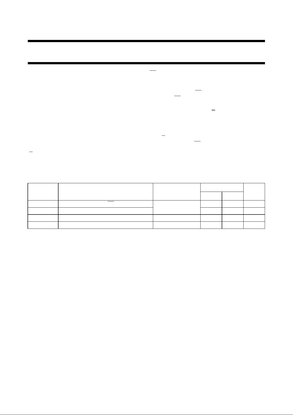
PIN DESCRIPTION
PIN NO. SYMBOL NAME AND FUNCTION
3, 2, 4, 7, 10, 1, 5, 6, 9, 11 Q
0
to Q
9
decoded outputs
8 GND ground (0 V)
12
Q
5-9
carry output (active LOW)
13
CP
1
clock input (HIGH-to-LOW, edge-triggered)
14 CP
0
clock input (LOW-to-HIGH, edge-triggered)
15 MR master reset input (active HIGH)
16 V
CC
positive supply voltage
Fig.1 Pin configuration.
Fig.2 Logic symbol. Fig.3 IEC logic symbol.
Page 4

December 1990 4
Philips Semiconductors Product specification
Johnson decade counter with 10 decoded outputs 74HC/HCT4017
FUNCTION TABLE
Notes
1. H = HIGH voltage level
L = LOW voltage level
X = don’t care
↑ = LOW-to-HIGH clock transition
↓ = HIGH-to-LOW clock transition
MR CP
0
CP
1
OPERATION
HXXQ
0=Q5-9
= H; Q1 to Q9=L
L
L
L
L
L
L
H
↑
L
X
H
↓
↓
L
X
H
↑
L
counter advances
counter advances
no change
no change
no change
no change
Fig.4 Functional diagram.
Page 5

December 1990 5
Philips Semiconductors Product specification
Johnson decade counter with 10 decoded
outputs
74HC/HCT4017
Fig.5 Logic diagram.
Fig.6 Timing diagram.
Page 6

December 1990 6
Philips Semiconductors Product specification
Johnson decade counter with 10 decoded outputs 74HC/HCT4017
DC CHARACTERISTICS FOR 74HC
For the DC characteristics see
“74HC/HCT/HCU/HCMOS Logic Family Specifications”
.
Output capability: standard
ICC category: MSI
Page 7

December 1990 7
Philips Semiconductors Product specification
Johnson decade counter with 10 decoded outputs 74HC/HCT4017
AC CHARACTERISTICS FOR 74HC
GND = 0 V; t
r=tf
= 6 ns; CL= 50 pF
SYMBOL
PARAMETER
T
amb
(°C)
UNIT
TEST CONDITIONS
74HC
V
CC
(V)
WAVEFORMS
+25 −40 to+85 −40 to+125
min. typ. max. min. max. min. max.
t
PHL
/ t
PLH
propagation delay
CP0 to Q
n
63
23
18
230
46
39
290
58
49
345
69
59
ns 2.0
4.5
6.0
Fig.9
t
PHL
/ t
PLH
propagation delay
CP0 to Q
5-9
63
23
18
230
46
39
290
58
49
345
69
59
ns 2.0
4.5
6.0
Fig.9
t
PHL
/ t
PLH
propagation delay
CP1 to Q
n
61
22
18
250
50
43
315
63
54
375
75
64
ns 2.0
4.5
6.0
Fig.9
t
PHL
/ t
PLH
propagation delay
CP1 to Q
5-9
61
22
18
250
50
43
315
63
54
375
75
64
ns 2.0
4.5
6.0
Fig.9
t
PHL
propagation delay
MR to Q
1−9
52
19
15
230
46
39
290
58
49
345
69
59
ns 2.0
4.5
6.0
Fig.8
t
PLH
propagation delay
MR to Q
5−9
, Q
0
55
20
16
230
46
39
290
58
49
345
69
59
ns 2.0
4.5
6.0
Fig.8
t
THL
/ t
TLH
output transition
time
19
7
6
75
15
13
95
19
16
110
22
19
ns 2.0
4.5
6.0
Fig.9
t
W
clock pulse width
HIGH or LOW
80
16
14
17
6
5
100
20
17
120
24
20
ns 2.0
4.5
6.0
Fig.8
t
W
master reset pulse
width; HIGH
80
16
14
19
7
6
100
20
17
120
24
20
ns 2.0
4.5
6.0
Fig.8
t
rem
removal time
MR to CP0, CP
1
5
5
5
−17
−6
−5
5
5
5
5
5
5
ns 2.0
4.5
6.0
Fig.8
t
su
set-up time
CP1 to CP0;
CP0 to CP
1
50
10
9
−8
−3
−2
65
13
11
75
15
13
ns 2.0
4.5
6.0
Fig.7
t
h
hold time
CP0 to CP1;
CP1 to CP
0
50
10
9
17
6
5
65
13
11
75
15
13
ns 2.0
4.5
6.0
Fig.7
f
max
maximum clock
pulse frequency
6.0
30
25
23
70
83
4.8
24
28
4.0
20
24
MHz 2.0
4.5
6.0
Fig.8
Page 8

December 1990 8
Philips Semiconductors Product specification
Johnson decade counter with 10 decoded outputs 74HC/HCT4017
DC CHARACTERISTICS FOR 74HCT
For the DC characteristics see
“74HC/HCT/HCU/HCMOS Logic Family Specifications”
.
Output capability: standard
ICC category: MSI
Note to HCT types
The value of additional quiescent supply current (∆ICC) for a unit load of 1 is given in the family specifications.
To determine ∆I
CC
per input, multiply this value by the unit load coefficient shown in the table below.
INPUT UNIT LOAD COEFFICIENT
CP
1
CP
0
MR
0.40
0.25
0.50
Page 9

December 1990 9
Philips Semiconductors Product specification
Johnson decade counter with 10 decoded outputs 74HC/HCT4017
AC CHARACTERISTICS FOR 74HCT
GND = 0 V; t
r=tf
= 6 ns; CL= 50 pF
SYMBOL PARAMETER
T
amb
(°C)
UNIT
TEST CONDITIONS
74HCT
V
CC
(V)
WAVEFORMS
+25 −40 to+85 −40 to+125
min. typ. max. min. max. min. max.
t
PHL
/ t
PLH
propagation delay
CP0 to Q
n
25 46 58 69 ns 4.5 Fig.9
t
PHL
/ t
PLH
propagation delay
CP0 to Q
5-9
25 46 58 69 ns 4.5 Fig.9
t
PHL
/ t
PLH
propagation delay
CP1 to Q
n
25 50 63 75 ns 4.5 Fig.9
t
PHL
/ t
PLH
propagation delay
CP1 to Q
5-9
25 50 63 75 ns 4.5 Fig.9
t
PHL
propagation delay
MR to Q
1−9
22 46 58 69 ns 4.5 Fig.8
t
PLH
propagation delay
MR to Q
5−9
, Q
0
20 46 58 69 ns 4.5 Fig.8
t
THL
/ t
TLH
output transition time 7 15 19 22 ns 4.5 Fig.9
t
W
clock pulse width
HIGH or LOW
16 7 20 24 ns 4.5 Fig.8
t
W
master reset pulse
width; HIGH
16 4 20 24 ns 4.5 Fig.8
t
rem
removal time
MR to CP0, CP
1
5 −5 5 5 ns 4.5 Fig.8
t
su
set-up time
CP1 to CP0;
CP0 to CP
1
10 −3 13 15 ns 4.5 Fig.7
t
h
hold time
CP0 to CP1;
CP1 to CP
0
10 6 13 15 ns 4.5 Fig.7
f
max
maximum clock pulse
frequency
30 61 24 20 ns 4.5 Fig.8
Page 10

December 1990 10
Philips Semiconductors Product specification
Johnson decade counter with 10 decoded outputs 74HC/HCT4017
AC WAVEFORMS
Fig.7 Waveforms showing the hold and set-up times for CP0 to CP1 and CP1 to CP0.
(1) HC : VM= 50%; VI= GND to V
CC
.
HCT: VM= 1.3 V; VI= GND to 3 V.
Fig.8 Waveforms showing the minimum pulse widths for CP0, CP1 and MR inputs; the recovery time for MR and
the propagation delays for MR to Qn and Q
5-9
outputs.
Conditions:
CP1= LOW while CP0 is triggered on a LOW-to-HIGH
transition and CP
0
= HIGH, while CP1 is triggered on a
HIGH-to-LOW transition.
(1) HC : V
M
= 50%; VI= GND to V
CC
.
HCT: VM= 1.3 V; VI= GND to 3 V.
Page 11

December 1990 11
Philips Semiconductors Product specification
Johnson decade counter with 10 decoded outputs 74HC/HCT4017
Fig.9 Waveforms showing the propagation delays for CP0, CP1 to Qn, Q
5-9
outputs and the output transition times.
Conditions:
CP1= LOW while CP0 is triggered on a LOW-to-HIGH transition
and CP
0
= HIGH, while CP1 is triggered on a HIGH-to-LOW
transition.
(1) HC : V
M
= 50%; VI= GND to V
CC
.
HCT: VM= 1.3 V; VI= GND to 3 V.
Page 12

December 1990 12
Philips Semiconductors Product specification
Johnson decade counter with 10 decoded outputs 74HC/HCT4017
APPLICATION INFORMATION
Some applications for the “4017” are:
• Decade counter with decimal decoding
• 1 out of n decoding counter (when cascaded)
• Sequential controller
• Timer
Figure 10 shows a technique for extending the number of decoded output states for the “4017”. Decoded outputs are
sequential within each stage and from stage to stage, with no dead time (except propagation delay).
Figure 11 shows an example of a divide-by 2 through divide-by 10 circuit using one “4017”. Since “4017” has an
asynchronous reset, the output pulse widths are narrow (minimum expected pulse width is 6 ns). The output pulse widths
can be enlarged by inserting a RC network at the MR input.
PACKAGE OUTLINES
See
“74HC/HCT/HCU/HCMOS Logic Package Outlines”
.
Fig.10 Counter expansion
It is essential not to enable the counter on CP
1
when CP0 is HIGH, or on CP0 when CP1 is LOW,
as this would cause an extra count.
Fig.11 Divide-by 2 through divide-by 10.
 Loading...