

Datasheet 74HCT40105U, 74HCT40105DB, 74HCT40105D, 74HC40105U, 74HC40105PW Datasheet (Philips)
...Page 1

DATA SH EET
Product specification
Supersedes data of December 1990
File under Integrated Circuits, IC06
1998 Jan 23
INTEGRATED CIRCUITS
74HC/HCT40105
4-bit x 16-word FIFO register
For a complete data sheet, please also download:
•The IC06 74HC/HCT/HCU/HCMOS Logic Family Specifications
Page 2

1998 Jan 23 2
Philips Semiconductors Product specification
4-bit x 16-word FIFO register 74HC/HCT40105
FEATURES
• Independent asynchronous inputs and outputs
• Expandable in either direction
• Reset capability
• Status indicators on inputs and outputs
• 3-state outputs
• Output capability: standard
• ICCcategory: MSI
GENERAL DESCRIPTION
The 74HC/HCT40105 are high-speed Si-gate CMOS
devices and are pin compatible with the “40105” of the
“4000B” series. They are specified in compliance with
JEDEC standard no. 7A.
The 74HC/HCT40105 are first-in/first-out (FIFO) “elastic”
storage registers that can store sixteen 4-bit words. The
“40105” is capable of handling input and output data at
different shifting rates. This feature makes it particularly
useful as a buffer between asynchronous systems. Each
word position in the register is clocked by a control flip-flop,
which stores a marker bit. A “1” signifies that the position’s
data is filled and a “0” denotes a vacancy in that position.
The control flip-flop detects the state of the preceding
flip-flop and communicates its own status to the
succeeding flip-flop. When a control flip-flop is in the “0”
state and sees a “1” in the preceding flip-flop, it generates
a clock pulse that transfers data from the preceding four
data latches into its own four data latches and resets the
preceding flip-flop to “0”. The first and last control flip-flops
have buffered outputs. Since all empty locations “bubble”
automatically to the input end, and all valid data ripples
through to the output end, the status of the first control
flip-flop (data-in ready output - DIR) indicates if the FIFO is
full, and the status of the last flip-flop (data-out ready
output - DOR) indicates if the FIFO contains data. As the
earliest data is removed from the bottom of the data stack
(output end), all data entered later will automatically ripple
toward the output.
QUICK REFERENCE DATA
GND = 0 V; T
amb
= 25 °C; tr= tf= 6 ns
Notes
1. C
PD
is used to determine the dynamic power dissipation (PDin µW):
PD= CPD× V
CC
2
× fi+∑(CL× V
CC
2
× fo) where:
fi= input frequency in MHz.
fo= output frequency in MHz.
∑ (CL× V
CC
2
× fo) = sum of outputs
CL= output load capacitance in pF
VCC= supply voltage in V
2. For HC the condition is VI= GND to V
CC
For HCT the condition is VI= GND to VCC− 1.5
SYMBOL PARAMETER CONDITIONS
TYP.
UNIT
HC HCT
t
PHL
/ t
PLH
propagation delay CL= 15 pF; VCC=5 V
MR to DIR, DOR 16 15 ns
SO to Q
n
37 35 ns
t
PHL
propagation delay
SI to DIR 16 18 ns
SO to DOR 17 18 ns
f
max
maximum clock frequency 33 31 MHz
C
I
input capacitance 3.5 3.5 pF
C
PD
power dissipation capacitance per package notes 1 and 2 134 145 pF
Page 3
1998 Jan 23 3
Philips Semiconductors Product specification
4-bit x 16-word FIFO register 74HC/HCT40105
ORDERING INFORMATION
PIN DESCRIPTION
TYPE NUMBER
PACKAGE
NAME DESCRIPTION VERSION
74HC(T)40105N DIP16 plastic dual in-line package; 16 leads (300 mil); long body SOT38-1
74HC(T)40105D SO16 plastic small outline package; 16 leads; body width 3.9 mm SOT109-1
74HC(T)40105DB SSOP16 plastic shrink small outline package; 16 leads; body width 5.3 mm SOT338-1
74HC(T)40105PW TSSOP16 plastic thin shrink small outline package; 16 leads; body width 4.4 mm SOT403-1
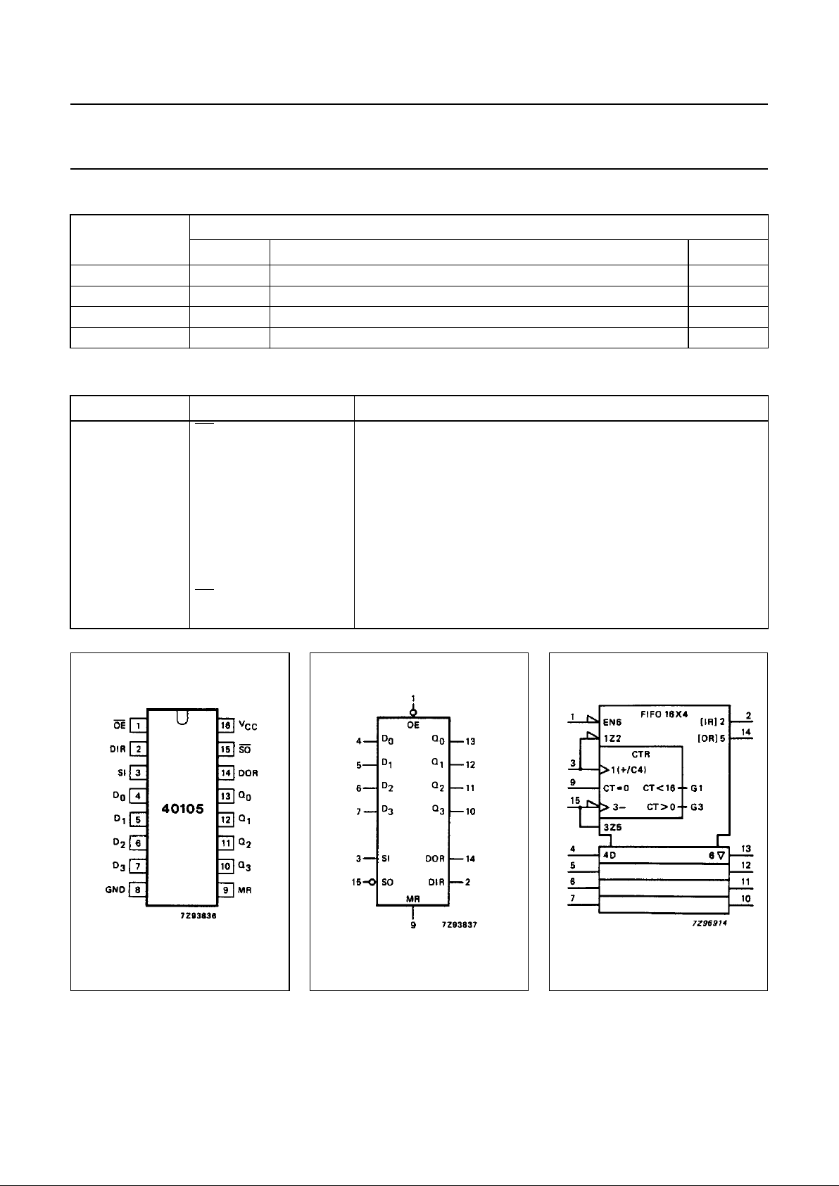
PIN NO. SYMBOL NAME AND FUNCTION
1
OE output enable input (active LOW)
2 DIR data-in ready output
3 SI shift-in input (LOW-to-HIGH, edge-triggered)
4, 5, 6, 7 D
0
to D
3
parallel data inputs
8 GND ground (0 V)
9 MR asynchronous master reset input (active HIGH)
13, 12, 11, 10 Q
0
to Q
3
3-state data outputs
14 DOR data-out ready output
15
SO shift-out input (HIGH-to-LOW, edge-triggered)
16 V
CC
positive supply voltage
Fig.1 Pin configuration. Fig.2 Logic symbol. Fig.3 IEC logic symbol.
Page 4

1998 Jan 23 4
Philips Semiconductors Product specification
4-bit x 16-word FIFO register 74HC/HCT40105
INPUT AND OUTPUTS
Data inputs (D
0
to D3)
As there is no weighting of the inputs,
any input can be assigned as the
MSB. The size of the FIFO memory
can be reduced from the 4 × 16
configuration, i.e. 3 × 16, down to
1 × 16, by tying unused data input
pins to V
CC
or GND.
Data outputs (Q
0
to Q3)
As there is no weighting of the
outputs, any output can be assigned
as the MSB. The size of the FIFO
memory can be reduced from the
4 × 16 configuration as described for
data inputs. In a reduced format, the
unused data outputs pins must be left
open circuit.
Master-reset (MR)
When MR is HIGH, the control
functions within the FIFO are cleared,
and date content is declared invalid.
The data-in ready (DIR) flag is set
HIGH and the data-out-ready (DOR)
flag is set LOW. The output stage
remains in the state of the last word
that was shifted out, or in the random
state existing at power-up.
Status flag outputs (DIR, DOR)
Indication of the status of the FIFO is
given by two status flags,
data-in-ready (DIR) and
data-out-ready (DOR):
DIR = HIGH indicates the input stage
is empty and ready to accept valid
data;
DIR = LOW indicates that the FIFO is
full or that a previous shift-in
operation is not complete (busy);
DOR = HIGH assures valid data is
present at the outputs Q
0
to Q3(does
not indicate that new data is awaiting
transfer into the output stage);
DOR = LOW indicates the output
stage is busy or there is no valid data.
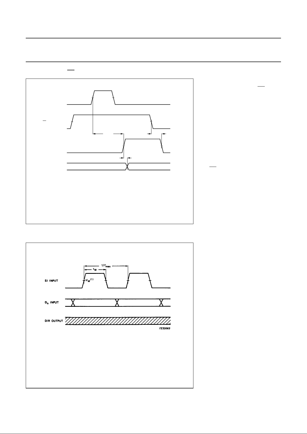
Shift-in control (SI)
Data is loaded into the input stage on
a LOW-to-HIGH transition of SI.
It also triggers an automatic data
transfer process (ripple through). If SI
is held HIGH during reset, data will be
loaded at the falling edge of the MR
signal.
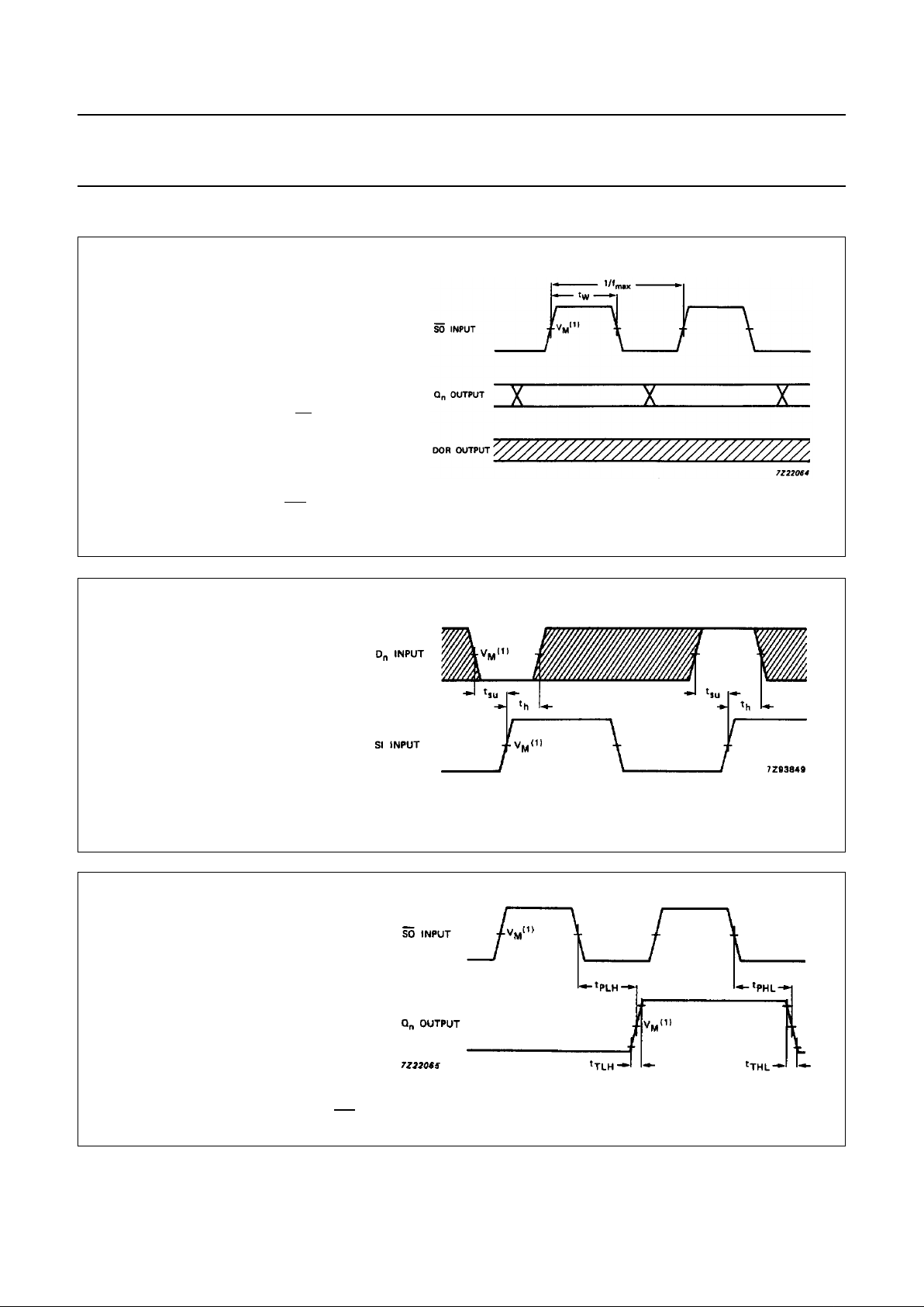
Shift-out control (
SO)
A HIGH-to-LOW transition of
SO causes the DOR flags to go LOW.
A HIGH-to-LOW transition of
SO causes upstream data to move
into the output stage, and empty
locations to move towards the input
stage (bubble-up).
Output enable (
OE)
The outputs Q0to Q3are enabled
when OE = LOW. When OE = HIGH
the outputs are in the high impedance
OFF-state.
FUNCTIONAL DESCRIPTION
Data input
Following power-up, the master-reset
(MR) input is pulsed HIGH to clear the
FIFO memory (see Fig.8). The
data-in-ready flag (DIR = HIGH)
indicates that the FIFO input stage is
empty and ready to receive data.
When DIR is valid (HIGH), data
present at D
0
to D3can be shifted-in
using the SI control input.
With SI = HIGH, data is shifted into
the input stage and a busy indication
is given by DIR going LOW.
The data remains at the first location
in the FIFO until DIR is set to HIGH
and data moves through the FIFO to
the output stage, or to the last empty
location. If the FIFO is not full after the
SI pulse, DIR again becomes valid
(HIGH) to indicate that space is
available in the FIFO. The DIR flag
remains LOW if the FIFO is full (see
Fig.6). The SI use must be made
LOW in order to complete the shift-in
process.
With the FIFO full, SI can be held
HIGH until a shift-out (
SO) pulse
occurs. Then, following a shift-out of
data, an empty location appears at
the FIFO input and DIR goes HIGH to
allow the next data to be shifted-in.
This remains at the first FIFO location
until SI goes LOW (see Fig.7).
Data transfer
After data has been transferred from
the input stage of the FIFO following
SI = LOW, data moves through the
FIFO asynchronously and is stacked
at the output end of the register.
Empty locations appear at the input
end of the FIFO as data moves
through the device.
Data output
The data-out-ready flag
(DOR = HIGH) indicates that there is
valid data at the output (Q
0
to Q3).
The initial master-reset at power-on
(MR = HIGH) sets DOR to LOW (see
Fig.8). After MR = LOW, data shifted
into the FIFO moves through to the
output stage causing DOR to go
HIGH.
As the DOR flag goes HIGH, data can
be shifted-out using the SO = HIGH,
data in the output stage is shifted out
and a busy indication is given by DOR
going LOW. When SO is made LOW,
data moves through the FIFO to fill
the output stage and an empty
location appears at the input stage.
When the output stage is filled DOR
goes HIGH, but if the last of the valid
data has been shifted-out leaving the
FIFO empty the DOR flag remains
LOW (see Fig.9). With the FIFO
empty, the last word that was
shifted-out is latched at the output
Q0to Q3.
With the FIFO empty, the SO input
can be held HIGH until the SI control
input is used. Following an SI pulse,
Page 5

1998 Jan 23 5
Philips Semiconductors Product specification
4-bit x 16-word FIFO register 74HC/HCT40105
data moves through the FIFO to the
output stage, resulting in the DOR
flag pulsing HIGH and a shift-out of
data occurring. The SO control must
be made LOW before additional data
can be shifted-out (see Fig.10).
High-speed burst mode
If it is assumed that the
shift-in/shift-out pulses are not
applied until the respective status
flags are valid, it follows that the
shift-in/shift-out rates are determined
by the status flags. However, without
the status flags a high-speed burst
mode can be implemented. In this
mode, the burst-in/ burst-out rates are
determined by the pulse widths of the
shift-in/shift-out inputs and burst rates
of 35 MHz can be obtained. Shift
pulses can be applied without regard
to the status flags but shift-in pulses
that would overflow the storage
capacity of the FIFO are not allowed
(see Figs 11 and 12).
Expanded format
With the addition of a logic gate, the
FIFO is easily expanded to increase
word length (see Fig.17). The basic
operation and timing are identical to a
single FIFO, with the exception of an
additional gate delay on the flag
outputs. If during application, the
following occurs:
• SI is held HIGH when the FIFO is
empty, some additional logic is
required to produce a composite
DIR pulse (see Figs 7 and 18).
Due to the part-to-part spread of the
ripple through time, the SI signals of
FIFOAand FIFOBwill not always
coincide and the AND-gate will not
produce a composite flag signal. The
solution is given in Fig.18.
The “40105” is easily cascaded to
increase the word capacity and no
external components are needed. In
the cascaded configuration, all
necessary communications and
timing are performed by the FIFOs.
The intercommunication speed is
determined by the minimum flag
pulse widths and the flag delays. The
data rate of cascaded devices is
typically 25 MHz. Word-capacity can
be expanded to and beyond 32-words
× 4-bits (see Fig.19).
Page 6

1998 Jan 23 6
Philips Semiconductors Product specification
4-bit x 16-word FIFO register 74HC/HCT40105
Fig.4 Functional diagram.
Fig.5 Logic diagram.
(see control flip-flops)
(1) LOW on S input of FF1, and FF5 will set Q output to HIGH independent of state on R input.
(2) LOW on R input of FF2, FF3 and FF4 will set Q output to LOW independent of state on S input.
Page 7
1998 Jan 23 7
Philips Semiconductors Product specification
4-bit x 16-word FIFO register 74HC/HCT40105
DC CHARACTERISTICS FOR 74HC
For the DC characteristics see
“74HC/HCT/HCU/HCMOS Logic Family Specifications”
.
Output capability: standard
ICCcategory: MSI
AC CHARACTERISTICS FOR 74HC
GND = 0 V; t
f
= tf= 6 ns; CL= 50 pF
SYMBOL PARAMETER
T
amb
(°C)
UNIT
TEST CONDITIONS
74HC
V
CC
(V)
WAVEFORMS
+25 −40 to +85 −40 to +125
min. typ. max. min. max. min. max.
t
PHL
/ t
PLH
propagation delay
MR to DIR, DOR
52 175 220 265 ns 2.0 Fig.8
19 35 44 53 4.5
15 30 37 45 6.0
t
PHL
propagation delay
SI to DIR
52 210 265 315 ns 2.0 Fig.6
19 42 53 63 4.5
15 36 45 54 6.0
t
PHL
propagation delay
SO to DOR
55 210 265 315 ns 2.0 Fig.9
20 42 53 63 4.5
16 36 45 54 6.0
t
PHL
/ t
PLH
propagation delay
SO to Q
n
116 400 500 600 ns 2.0 Fig.14
42 80 100 120 4.5
34 68 85 102 6.0
t
PLH
propagation delay/
ripple through delay
SI to DOR
564 2000 2500 3000 ns 2.0 Fig.10
205 400 500 600 4.5
165 340 425 510 6.0
t
PLH
propagation delay/
bubble-up delay
SO to DIR
701 2500 3125 3750 ns 2.0 Fig.7
255 500 625 750 4.5
204 425 532 638 6.0
t
PZH
/ t
PZL
3-state output enable time
OE to Q
n
41 150 190 225 ns 2.0 Fig.16
15 30 38 45 4.5
12 26 33 38 6.0
t
PHZ
/ t
PLZ
3-state output disable
time
OE to Q
n
41 140 175 210 ns 2.0 Fig.16
15 28 35 42 4.5
12 24 30 36 6.0
t
THL
/ t
TLH
output transition time 19 75 95 110 ns 2.0 Fig.14
7 15 19 22 4.5
6 13 16 19 6.0
t
W
SI pulse width
HIGH or LOW
80 19 100 120 ns 2.0 Fig.6
16 7 20 24 4.5
14 6 17 20 6.0
Page 8

1998 Jan 23 8
Philips Semiconductors Product specification
4-bit x 16-word FIFO register 74HC/HCT40105
t
W
SO pulse width
HIGH or LOW
120 39 150 180 ns 2.0 Fig.9
24 14 30 36 4.5
20 11 26 31 6.0
t
W
DIR pulse width
HIGH
12 58 180 10 225 10 270 ns 2.0 Fig.7
6 21 36 5 45 5 54 4.5
5 17 31 4 38 4 46 6.0
t
W
DOR pulse width
LOW
12 55 170 10 215 10 255 ns 2.0 Fig.9
6 20 34 5 43 5 51 4.5
5 16 29 4 37 4 43 6.0
t
W
MR pulse width
HIGH
80 22 100 120 ns 2.0 Fig.8
16 8 20 24 4.5
14 6 17 20 6.0
t
rem
removal time
MR to SI
50 14 65 75 ns 2.0 Fig.15
10 5 13 15 4.5
9 4 11 13 6.0
t
su
set-up time
Dn to SI
−5 −39 −5 −5 ns 2.0 Fig.13
−5 −14 −5 −5 4.5
−5 −11 −5 −5 6.0
t
h
hold time
Dnto SI
125 44 155 190 ns 2.0 Fig.13
25 16 31 38 4.5
21 13 26 32 6.0
f
max
maximum pulse
frequency
SI, SO using flags or
burst mode
3.6 10 2.8 2.4 MHz 2.0 Fig.6, 9, 11
and 12
18 30 14 12 4.5
21 36 16 14 6.0
f
max
maximum pulse
frequency
SI, SO cascaded
3.6 10 2.8 2.4 MHz 2.0 Figs 6 and 9
18 30 14 12 4.5
21 36 16 14 6.0
SYMBOL PARAMETER
T
amb
(°C)
UNIT
TEST CONDITIONS
74HC
V
CC
(V)
WAVEFORMS
+25 −40 to +85 −40 to +125
min. typ. max. min. max. min. max.
Page 9

1998 Jan 23 9
Philips Semiconductors Product specification
4-bit x 16-word FIFO register 74HC/HCT40105
DC CHARACTERISTICS FOR 74HCT
For the DC characteristics see
“74HC/HCT/HCU/HCMOS Logic Family Specifications”
.
Output capability: standard
ICCcategory: MSI
Note to HCT types
The value of additional quiescent supply current (∆I
CC
) for a unit load of 1 is given in the family specifications.
To determine ∆I
CC
per input, multiply this value by the unit load coefficient shown in the table below.
AC CHARACTERISTICS FOR 74HCT
GND = 0 V; t
f
= tf= 6 ns; CL= 50 pF
INPUT UNIT LOAD COEFFICIENT
OE 0.75
SI 0.40
D
n
0.30
MR 1.50
SO 0.40
SYMBOL PARAMETER
T
amb
(°C)
UNIT
TEST CONDITIONS
74HCT
V
CC
(V)
WAVEFORMS
+25 −40 to +85 −40 to +125
min. typ. max. min. max. min. max.
t
PHL
/ t
PLH
propagation delay
MR to DIR, DOR
18 35 44 53 ns 4.5 Fig.8
t
PHL
propagation delay
SI to DIR
21 42 53 63 ns 4.5 Fig.6
t
PHL
propagation delay
SO to DOR
20 42 53 63 ns 4.5 Fig.9
t
PHL
/ t
PLH
propagation delay
SO to Q
n
40 80 100 120 ns 4.5 Fig.14
t
PLH
propagation delay/
ripple through delay
SI to DOR
188 400 500 600 ns 4.5 Fig.10
t
PLH
propagation delay/
bubble-up delay
SO to DIR
244 500 625 750 ns 4.5 Fig.7
t
PZH
/ t
PZL
3-state output enable time
OE to Q
n
18 35 44 53 ns 4.5 Fig.16
t
PHZ
/ t
PLZ
3-state output disable
time
OE to Q
n
15 30 38 45 ns 4.5 Fig.16
t
THL
/ t
TLH
output transition time 7 15 19 22 ns 4.5 Fig.14
Page 10

1998 Jan 23 10
Philips Semiconductors Product specification
4-bit x 16-word FIFO register 74HC/HCT40105
t
W
SI pulse width
HIGH or LOW
16 6 20 24 ns 4.5 Fig.6
t
W
SO pulse width
HIGH or LOW
16 7 20 24 ns 4.5 Fig.9
t
W
DIR pulse width
HIGH or LOW
6 20 34 5 43 5 51 ns 4.5 Fig.7
t
W
DOR pulse width
HIGH or LOW
6 19 34 5 43 5 51 ns 4.5 Fig.9
t
W
MR pulse width
HIGH
16 7 20 24 ns 4.5 Fig.8
t
rem
removal time
MR to SI
15 7 19 22 ns 4.5 Fig.15
t
su
set-up time
Dn to SI
−5 −14 −4 −4 ns 4.5 Fig.13
t
h
hold time
Dnto SI
27 16 34 41 ns 4.5 Fig.13
f
max
maximum pulse frequency
SI, SO using flags or
burst mode
28 12 10 MHz 4.5 Fig.6, 9, 11 and
12
f
max
maximum pulse frequency
SI, SO cascaded
28 12 10 MHz 4.5 Figs 6 and 9
SYMBOL PARAMETER
T
amb
(°C)
UNIT
TEST CONDITIONS
74HCT
V
CC
(V)
WAVEFORMS
+25 −40 to +85 −40 to +125
min. typ. max. min. max. min. max.
Page 11

1998 Jan 23 11
Philips Semiconductors Product specification
4-bit x 16-word FIFO register 74HC/HCT40105
AC WAVEFORMS
Shifting in sequence FIFO empty to FIFO full
Fig.6 Waveforms showing the SI input to DIR output propagation
delay. The SI pulse width and SI maximum pulse frequency.
(1) HC : VM= 50%; VI= GND to VCC.
HCT : V
M
= 1.3 V; VI= GND to 3 V.
Notes to Fig.6
1. DIR initially HIGH; FIFO is
prepared for valid data.
2. SI set HIGH; data loaded into
input stage.
3. DIR drops LOW, input stage
“busy”.
4. DIR goes HIGH, status flag
indicates FIFO prepared for
additional data; data from first
location “ripple through”.
5. SI set LOW; necessary to
complete shift-in process.
6. Repeat process to load 2nd word
through to 16th word into FIFO.
7. DIR remains LOW: with attempt
to shift into full FIFO, no data
transfer occurs.
With FIFO full; SI held HIGH in anticipation of empty location
Fig.7 Waveforms showing bubble-up delay, SO input to DIR output
and DIR output pulse width.
(1) HC : VM= 50%; VI= GND to VCC.
HCT : V
M
= 1.3 V; VI= GND to 3 V.
Notes to Fig.7
1. FIFO is initially, shift-in is held
HIGH.
2. SO pulse; data in the output
stage is unloaded, “bubble-up
process of empty locations
begins”.
3. DIR HIGH; when empty location
reached input stage, flag
indicates FIFO is prepared for
data input.
4. DIR returns to LOW; FIFO is full
again.
5. SI brought LOW; necessary to
complete whidt-in process, DIR
remains LOW, because FIFO is
full.
Page 12

1998 Jan 23 12
Philips Semiconductors Product specification
4-bit x 16-word FIFO register 74HC/HCT40105
Master reset applied with FIFO full
Fig.8 Waveforms showing the MR input to DIR, DOR output
propagation delays and the MR pulse width.
(1) HC : VM= 50%; VI= GND to VCC.
HCT : V
M
= 1.3 V; VI= GND to 3 V.
Notes to Fig.8
1. DIR LOW, output ready HIGH;
assume FIFO is full.
2. MR pulse HIGH; clears FIFO.
3. DIR goes HIGH; flag indicates
input prepared for valid data.
4. DOR drops LOW; flag indicates
FIFO empty.
Shifting out sequence; FIFO full to FIFO empty
Fig.9 Waveforms showing the SO input to DIR output propagation
delay. The SO pulse width and SO maximum pulse frequency.
(1) HC : VM= 50%; VI= GND to VCC.
HCT : V
M
= 1.3 V; VI= GND to 3 V.
Notes to Fig.9
1. DOR HIGH; no data transfer in
progress, valid data is present at
output stage.
2. SO set HIGH.
3. SO is set LOW; data in the input
stage is unloaded, and new data
replaces it as empty location
“bubbles-up” to input stage.
4. DOR drops LOW; output stage
“busy”.
5. DOR goes HIGH; transfer
process completed, valid data
present at output after the
specified propagation delay.
6. Repeat process to unloaded the
3rd through to the 16th word from
FIFO.
7. DOR remains LOW; FIFO is
empty.
Page 13
1998 Jan 23 13
Philips Semiconductors Product specification
4-bit x 16-word FIFO register 74HC/HCT40105
With FIFO empty; SO is held HIGH in anticipation
Fig.10 Waveforms showing ripple through delay SI input to DOR output
and propagation delay from the DOR pulse to the Qnoutput.
(1) HC : VM= 50%; VI= GND to VCC.
HCT : V
M
= 1.3 V; VI= GND to 3 V.
agewidth
MBA337
t
PHL
/ t
PLH
V
M
(1)
SI INPUT
SO INPUT
DOR OUTPUT
Q OUTPUT
n
V
M
(1)
V
M
(1)
2
1
t
PLH
ripple through
delay
4
5
6
t
PHL
3
Notes to Fig.10
1. FIFO is initially empty, SO is held
HIGH.
2. SI pulse; loads data into FIFO
and initiates ripple through
process.
3. DOR flag signals the arrival of
valid data at the output stage.
4. Output transition; data arrives at
output stage after the specified
propagation delay between the
rising edge of the DOR pulse to
the Q
n
output.
5. SO set LOW; necessary to
complete shift-out process. DOR
remains LOW, because FIFO is
empty.
6. DOR goes LOW; FIFO is empty
again.
Shift-in operation; high-speed burst mode
Fig.11 Waveforms showing SI minimum pulse width and SI maximum
pulse frequency, in high-speed shift-in burst mode.
(1) HC : VM= 50%; VI= GND to VCC.
HCT : V
M
= 1.3 V; VI= GND to 3 V.
Note to Fig.11
In the high-speed mode, the burst-in
rate is determined by the minimum
shift-in HIGH and shift-in LOW
specifications. The DIR status flag is
a don’t care condition, and a shift-in
pulse can be applied regardless of the
flag. A SI pulse which would overflow
the storage capacity of the FIFO is
ignored.
Page 14
1998 Jan 23 14
Philips Semiconductors Product specification
4-bit x 16-word FIFO register 74HC/HCT40105
Shift-out operation; high-speed burst mode
Fig.12 Waveforms showing SO minimum pulse width and maximum pulse frequency, in high-speed shift-out
burst mode.
In the high-speed mode, the burst-out rate is determined by the
minimum shift-out HIGH and shift-out LOW specifications. The
DOR flag is a don’t care condition and a
SO pulse can be applied
without regard to the flag.
(1) HC : V
M
= 50%; VI= GND to VCC.
HCT : V
M
= 1.3 V; VI= GND to 3 V.
Fig.13 Waveforms showing hold and set up times for Dninput to SI input.
The shaded areas indicate when the input is permitted
to change for predictable output performance.
(1) HC : V
M
= 50%; VI= GND to VCC.
HCT : V
M
= 1.3 V; VI= GND to 3 V.
Fig.14 Waveforms showing SO input to Qnoutput propagation delays and output transition time.
(1) HC : VM= 50%; VI= GND to VCC.
HCT : V
M
= 1.3 V; VI= GND to 3 V.
Page 15

1998 Jan 23 15
Philips Semiconductors Product specification
4-bit x 16-word FIFO register 74HC/HCT40105
Fig.15 Waveforms showing the MR input to SI input removal time.
(1) HC : VM= 50%; VI= GND to VCC.
HCT : V
M
= 1.3 V; VI= GND to 3 V.
handbook, halfpage
MBA332
V
M
(1)
V
M
(1)
t
rem
MR INPUT
SI INPUT
Fig.16 Waveforms showing the 3-state enable and disable times for input OE.
(1) HC : VM= 50%; VI= GND to VCC.
HCT : V
M
= 1.3 V; VI= GND to 3 V.
Page 16

1998 Jan 23 16
Philips Semiconductors Product specification
4-bit x 16-word FIFO register 74HC/HCT40105
APPLICATION INFORMATION
Fig.17 Expanded FIFO for increased word length; 16 words × 8 bits.
The PC74HC/HCT40105 is easily expanded to
increase word length. Composite DIR and DOR
flags are formed with the addition of an AND
gate. The basic operation and timing are
identical to a single FIFO, with the exception of
an added gate delay on the flags.
Fig.18 Expanded FIFO for increased word length.
This circuit is only required if the SI input is constantly held HIGH, when the FIFO is empty and the automatic shift-in cycles are started (see Fig.7).
Page 17

1998 Jan 23 17
Philips Semiconductors Product specification
4-bit x 16-word FIFO register 74HC/HCT40105
Expanded format
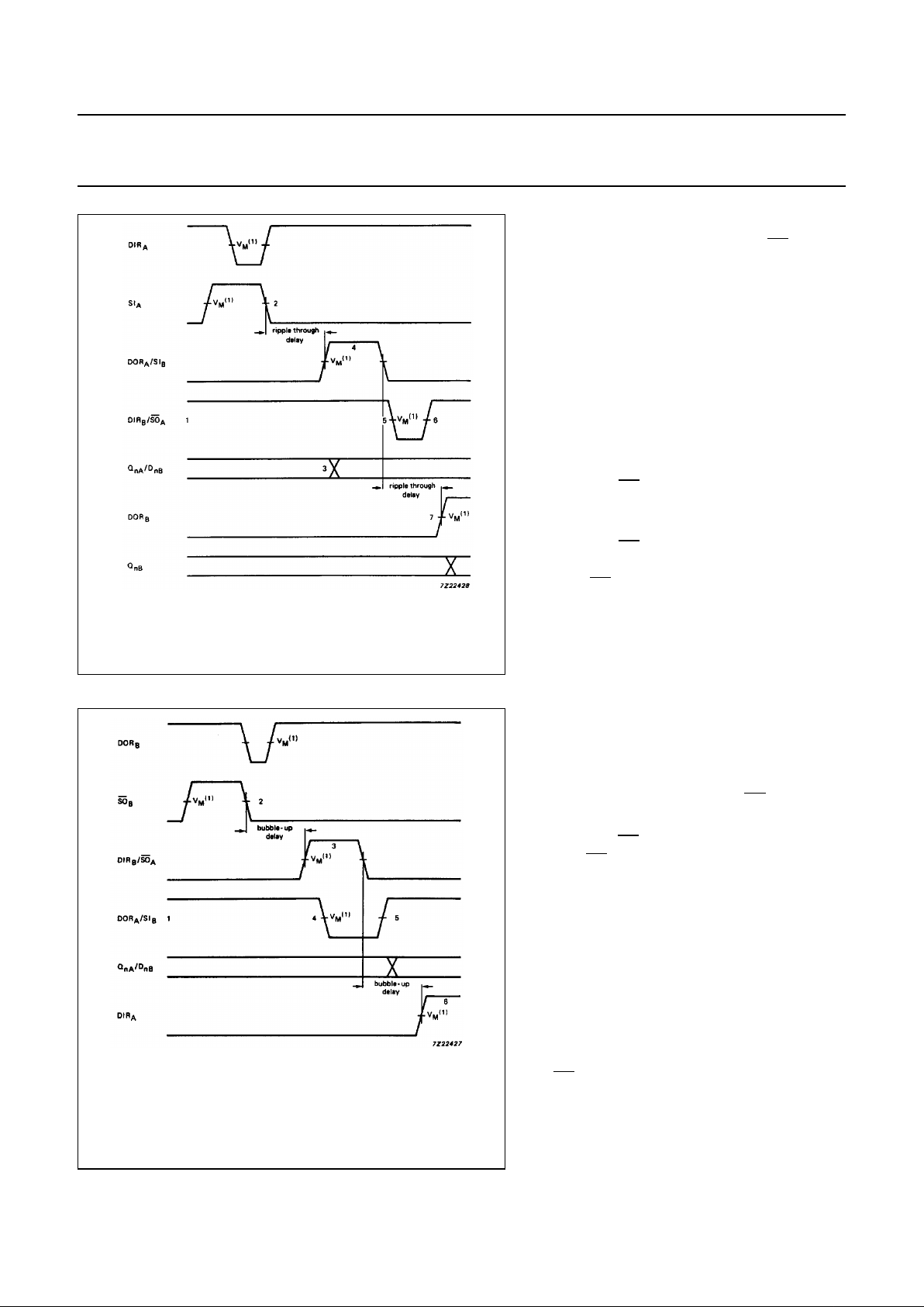
Fig.19 shows two cascaded FIFOs providing a capacity of 32 words × 4 bits
Fig.20 shows the signals on the nodes of both FIFOs after the application of a SI pulse, when both FIFOs are initially
empty. After a rippled through delay, date arrives at the output of FIFOA. Due to SOAbeing HIGH, a DOR pulse is
generated. The requirements of SIBand DnBare satisfied by the DORApulse width and the timing between the rising
edge of DORAand QnA. After a second ripple through delay, data arrives at the output of FIFOB.
Fig.21 shows the signals on the nodes of both FIFOs after the application of a SORpulse, when both FIFOs are initially
full. After a bubble-up delay a DIRRpulse is generated, which acts as a SOApulse for FIFOA. One word is transferred
from the output of FIFOAto the input of FIFOB. The requirements of the SOApulse for FIFOAis satisfied by the pulse
width of DORB. After a second bubble-up delay an empty space arrives at DnA, at which time DIRAgoes HIGH.
Fig.22 shows the waveforms at all external nodes of both FIFOs during a complete shift-in and shift-out sequence.
Fig.19 Cascading for increased word capacity; 32 words × 4 bits.
The PC7HC/HCT40105 is easily cascaded to increase word capacity without any external circuitry. In cascaded format, all necessary
communications are handled by the FIFOs. Figs 17 and 19 demonstrate the intercommunication timing between FIFO
A
and FIFOB. Fig.22 gives an
overview of pulse and timing of two cascaded FIFOs, when shifted full and shifted empty again.
Page 18
1998 Jan 23 18
Philips Semiconductors Product specification
4-bit x 16-word FIFO register 74HC/HCT40105
Fig.20 FIFO to FIFO communication; input timing under
empty condition.
(1) HC : VM= 50%; VI= GND to VCC.
HCT : V
M
= 1.3 V; VI= GND to 3 V.
Notes to Fig.20
1. FIFOAand FIFOBinitially empty, SOAheld
HIGH in anticipation of data.
2. Load one word into FIFOA; SI pulse applied,
results in DIR pulse.
3. Data outA/data inBtransition; valid data
arrives at FIFOAoutput stage after a specified
delay of the DOR flag, meeting data input
set-up requirements of FIFOB.
4. DORAand SIBpulse HIGH; (ripple through
delay after SI
A
LOW) data is unloaded from
FIFOA as a result of the data output ready
pulse, data is shifted into FIFOB.
5. DIRBand SOAgo LOW; flag indicates input
stage of FIFOBis busy, shift-out of FIFOAis
complete.
6. DIRBand SOAgo HIGH automatically; the
input stage of FIFOBis again able to receive
data, SO is held HIGH in anticipation of
additional data.
7. DORBgoes HIGH; (ripple through delay after
SIBLOW) valid data is present one
propagation delay later at the FIFOBoutput
stage.
(1) HC : VM= 50%; VI= GND to VCC.
HCT : V
M
= 1.3 V; VI= GND to 3 V.
Fig.21 FIFO to FIFO communication; output timing under
full condition.
Notes to Fig.21
1. FIFOAand FIFOBinitially empty, SIBheld
HIGH in anticipation of shifting in new data as
empty location bubbles-up.
2. Unload one word into FIFOB; SO pulse
applied, results in DOR pulse.
3. DIRB and SOApulse HIGH; (bubble-up delay
after SOBLOW) data is loaded into FIFOBas
a result of the DIR pulse, data is shifted out of
FIFOA.
4. DOR
A
and SIBgo LOW; flag indicates the
output stage of FIFOAis busy, shift-in to
FIFORis complete.
5. DORAand SIBgo HIGH; flag indicates valid
data is again available at FIFOAoutput stage,
SIBis held HIGH, awaiting bubble-up of
empty location.
6. DIRAgoes HIGH; (bubble-up delay after
SOALOW) an empty location is present at
input stage of FIFOA.
Page 19

1998 Jan 23 19
Philips Semiconductors Product specification
4-bit x 16-word FIFO register 74HC/HCT40105
Fig.22 Waveforms
showing the
functionally and
intercommunication
between two
FIFOs
(refer to Fig.19).
Note to Fig.22
Sequence 1 (Both FIFOs empty, starting shift-in process):
After a MR pulse has been applied FIFOAand FIFOBare
empty. The DOR flags of FIFOAand FIFOBgo LOW due
to no valid data being present at the outputs. The DIR flags
are set HIGH due to the FIFOs being ready to accept data.
SOBis held HIGH and two SIApulses are applied (1).
These pulses allow two data words to ripple through to the
output stage of FIFOAand to the input stage of FIFOB(2).
When data arrives at the output of FIFOB, a DORBpulse is
generated (3). When
SOBgoes LOW, the first bit is shifted
out and a second bit ripples through to the output after
which DORBgoes HIGH (4).
Sequence 2 (FIFOBruns full):
After the MR pulse, a series of 16 SI pulses are applied.
When 16 words are shifted in, DIRBremains LOW due to
FIFOBbeing full (5). DORAgoes LOW due to FIFOAbeing
empty.
Sequence 3 (FIFOAruns full):
When 17 words are shifted in, DORAremains HIGH due to
valid data remaining at the output of FIFOA.QnAremains
HIGH, being the polarity of the 17th data word (6). After the
32th SI pulse, DIR remains LOW and both FIFOs are full
(7). Additional pulses have no effect.
Sequence 4 (Both FIFOs full, starting shift-out process):
SI
A
is held HIGH and two SOBpulses are applied (8).
These pulses shift out two words and thus allow empty
locations to bubble-up to the input stage of FIFOB, and
proceed to FIFOA(9). When the first empty location arrives
at the input of FIFOA, a DIRApulse is generated (10) and
a new word is shifted into FIFOA.SIAis made LOW and
now the second empty location reaches the input stage of
FIFOA, after which DIRAremains HIGH (11).
Sequence 5 (FIFOAruns empty):
At the start of sequence 5 FIFOAcontains 15 valid words
due to two words being shifted out and one word being
shifted in sequence 4. An additional series of SOBpulses
are applied. After 15SOBpulses, all words from FIFOAare
shifted into FIFOB. DORAremains LOW (12).
Sequence 6 (FIFOBruns empty):
After the next SOBpulse, DIRBremains HIGH due to the
input stage of FIFOBbeing empty (13). After another 15
SOBpulses, DORBremains LOW due to both FIFOs being
empty (14). Additional SOBpulses have no effect. The last
word remains available at the output Qn.
Page 20

1998 Jan 23 20
Philips Semiconductors Product specification
4-bit x 16-word FIFO register 74HC/HCT40105
PACKAGE OUTLINES
UNIT
A
max.
1 2
b
1
cEe M
H
L
REFERENCES
OUTLINE
VERSION
EUROPEAN
PROJECTION
ISSUE DATE
IEC JEDEC EIAJ
mm
inches
DIMENSIONS (inch dimensions are derived from the original mm dimensions)
SOT38-1
92-10-02
95-01-19
A
min.
A
max.
b
max.
w
M
E
e
1
1.40
1.14
0.055
0.045
0.53
0.38
0.32
0.23
21.8
21.4
0.86
0.84
6.48
6.20
0.26
0.24
3.9
3.4
0.15
0.13
0.2542.54 7.62
0.30
8.25
7.80
0.32
0.31
9.5
8.3
0.37
0.33
2.2
0.087
4.7 0.51 3.7
0.15
0.021
0.015
0.013
0.009
0.010.100.0200.19
050G09 MO-001AE
M
H
c
(e )
1
M
E
A
L
seating plane
A
1
w M
b
1
e
D
A
2
Z
16
1
9
8
b
E
pin 1 index
0 5 10 mm
scale
Note
1. Plastic or metal protrusions of 0.25 mm maximum per side are not included.
(1) (1)
D
(1)
Z
DIP16: plastic dual in-line package; 16 leads (300 mil); long body
SOT38-1
Page 21

1998 Jan 23 21
Philips Semiconductors Product specification
4-bit x 16-word FIFO register 74HC/HCT40105
X
w M
θ
A
A
1
A
2
b
p
D
H
E
L
p
Q
detail X
E
Z
e
c
L
v M
A
(A )
3
A
8
9
1
16
y
pin 1 index
UNIT
A
max.
A1A2A
3
b
p
cD
(1)E(1) (1)
eHELLpQZywv θ
REFERENCES
OUTLINE
VERSION
EUROPEAN
PROJECTION
ISSUE DATE
IEC JEDEC EIAJ
mm
inches
1.75
0.25
0.10
1.45
1.25
0.25
0.49
0.36
0.25
0.19
10.0
9.8
4.0
3.8
1.27
6.2
5.8
0.7
0.6
0.7
0.3
8
0
o
o
0.25 0.1
DIMENSIONS (inch dimensions are derived from the original mm dimensions)
Note
1. Plastic or metal protrusions of 0.15 mm maximum per side are not included.
1.0
0.4
SOT109-1
95-01-23
97-05-22
076E07S MS-012AC
0.069
0.010
0.004
0.057
0.049
0.01
0.019
0.014
0.0100
0.0075
0.39
0.38
0.16
0.15
0.050
1.05
0.041
0.244
0.228
0.028
0.020
0.028
0.012
0.01
0.25
0.01 0.004
0.039
0.016
0 2.5 5 mm
scale
SO16: plastic small outline package; 16 leads; body width 3.9 mm
SOT109-1
Page 22
1998 Jan 23 22
Philips Semiconductors Product specification
4-bit x 16-word FIFO register 74HC/HCT40105
UNIT A1A2A
3
b
p
cD
(1)E(1)
eHELLpQZywv θ
REFERENCES
OUTLINE
VERSION
EUROPEAN
PROJECTION
ISSUE DATE
IEC JEDEC EIAJ
mm
0.21
0.05
1.80
1.65
0.25
0.38
0.25
0.20
0.09
6.4
6.0
5.4
5.2
0.65 1.25
7.9
7.6
1.03
0.63
0.9
0.7
1.00
0.55
8
0
o
o
0.130.2 0.1
DIMENSIONS (mm are the original dimensions)
Note
1. Plastic or metal protrusions of 0.25 mm maximum per side are not included.
SOT338-1
94-01-14
95-02-04
(1)
w M
b
p
D
H
E
E
Z
e
c
v M
A
X
A
y
1
8
16
9
θ
A
A
1
A
2
L
p
Q
detail X
L
(A )
3
MO-150AC
pin 1 index
0 2.5 5 mm
scale
SSOP16: plastic shrink small outline package; 16 leads; body width 5.3 mm
SOT338-1
A
max.
2.0
Page 23

1998 Jan 23 23
Philips Semiconductors Product specification
4-bit x 16-word FIFO register 74HC/HCT40105
UNIT A1A2A
3
b
p
cD
(1)E(2) (1)
eHELLpQZywv θ
REFERENCES
OUTLINE
VERSION
EUROPEAN
PROJECTION
ISSUE DATE
IEC JEDEC EIAJ
mm
0.15
0.05
0.95
0.80
0.30
0.19
0.2
0.1
5.1
4.9
4.5
4.3
0.65
6.6
6.2
0.4
0.3
0.40
0.06
8
0
o
o
0.13 0.10.21.0
DIMENSIONS (mm are the original dimensions)
Notes
1. Plastic or metal protrusions of 0.15 mm maximum per side are not included.
2. Plastic interlead protrusions of 0.25 mm maximum per side are not included.
0.75
0.50
SOT403-1 MO-153
94-07-12
95-04-04
w M
b
p
D
Z
e
0.25
18
16
9
θ
A
A
1
A
2
L
p
Q
detail X
L
(A )
3
H
E
E
c
v M
A
X
A
y
0 2.5 5 mm
scale
TSSOP16: plastic thin shrink small outline package; 16 leads; body width 4.4 mm
SOT403-1
A
max.
1.10
pin 1 index
Page 24

1998 Jan 23 24
Philips Semiconductors Product specification
4-bit x 16-word FIFO register 74HC/HCT40105
SOLDERING
Introduction
There is no soldering method that is ideal for all IC
packages. Wave soldering is often preferred when
through-hole and surface mounted components are mixed
on one printed-circuit board. However, wave soldering is
not always suitable for surface mounted ICs, or for
printed-circuits with high population densities. In these
situations reflow soldering is often used.
This text gives a very brief insight to a complex technology.
A more in-depth account of soldering ICs can be found in
our
“IC Package Databook”
(order code 9398 652 90011).
DIP
SOLDERING BY DIPPING OR BY WA VE
The maximum permissible temperature of the solder is
260 °C; solder at this temperature must not be in contact
with the joint for more than 5 seconds. The total contact
time of successive solder waves must not exceed
5 seconds.
The device may be mounted up to the seating plane, but
the temperature of the plastic body must not exceed the
specified maximum storage temperature (T
stg max
). If the
printed-circuit board has been pre-heated, forced cooling
may be necessary immediately after soldering to keep the
temperature within the permissible limit.
R
EPAIRING SOLDERED JOINTS
Apply a low voltage soldering iron (less than 24 V) to the
lead(s) of the package, below the seating plane or not
more than 2 mm above it. If the temperature of the
soldering iron bit is less than 300 °C it may remain in
contact for up to 10 seconds. If the bit temperature is
between 300 and 400 °C, contact may be up to 5 seconds.
SO, SSOP and TSSOP
REFLOW SOLDERING
Reflow soldering techniques are suitable for all SO, SSOP
and TSSOP packages.
Reflow soldering requires solder paste (a suspension of
fine solder particles, flux and binding agent) to be applied
to the printed-circuit board by screen printing, stencilling or
pressure-syringe dispensing before package placement.
Several techniques exist for reflowing; for example,
thermal conduction by heated belt. Dwell times vary
between 50 and 300 seconds depending on heating
method.
Typical reflow temperatures range from 215 to 250 °C.
Preheating is necessary to dry the paste and evaporate
the binding agent. Preheating duration: 45 minutes at
45 °C.
W
AVE SOLDERING
Wave soldering can be used for all SO packages. Wave
soldering is not recommended for SSOP and TSSOP
packages, because of the likelihood of solder bridging due
to closely-spaced leads and the possibility of incomplete
solder penetration in multi-lead devices.
If wave soldering is used - and cannot be avoided for
SSOP and TSSOP packages - the following conditions
must be observed:
• A double-wave (a turbulent wave with high upward
pressure followed by a smooth laminar wave) soldering
technique should be used.
• The longitudinal axis of the package footprint must be
parallel to the solder flow and must incorporate solder
thieves at the downstream end.
Even with these conditions:
• Only consider wave soldering SSOP packages that
have a body width of 4.4 mm, that is
SSOP16 (SOT369-1) or SSOP20 (SOT266-1).
• Do not consider wave soldering TSSOP packages
with 48 leads or more, that is TSSOP48 (SOT362-1)
and TSSOP56 (SOT364-1).
During placement and before soldering, the package must
be fixed with a droplet of adhesive. The adhesive can be
applied by screen printing, pin transfer or syringe
dispensing. The package can be soldered after the
adhesive is cured.
Maximum permissible solder temperature is 260 °C, and
maximum duration of package immersion in solder is
10 seconds, if cooled to less than 150 °C within
6 seconds. Typical dwell time is 4 seconds at 250 °C.
A mildly-activated flux will eliminate the need for removal
of corrosive residues in most applications.
R
EPAIRING SOLDERED JOINTS
Fix the component by first soldering two diagonallyopposite end leads. Use only a low voltage soldering iron
(less than 24 V) applied to the flat part of the lead. Contact
time must be limited to 10 seconds at up to 300 °C. When
using a dedicated tool, all other leads can be soldered in
one operation within 2 to 5 seconds between
270 and 320 °C.
Page 25

1998 Jan 23 25
Philips Semiconductors Product specification
4-bit x 16-word FIFO register 74HC/HCT40105
DEFINITIONS
LIFE SUPPORT APPLICATIONS
These products are not designed for use in life support appliances, devices, or systems where malfunction of these
products can reasonably be expected to result in personal injury. Philips customers using or selling these products for
use in such applications do so at their own risk and agree to fully indemnify Philips for any damages resulting from such
improper use or sale.
Data sheet status
Objective specification This data sheet contains target or goal specifications for product development.
Preliminary specification This data sheet contains preliminary data; supplementary data may be published later.
Product specification This data sheet contains final product specifications.
Limiting values
Limiting values given are in accordance with the Absolute Maximum Rating System (IEC 134). Stress above one or
more of the limiting values may cause permanent damage to the device. These are stress ratings only and operation
of the device at these or at any other conditions above those given in the Characteristics sections of the specification
is not implied. Exposure to limiting values for extended periods may affect device reliability.
Application information
Where application information is given, it is advisory and does not form part of the specification.
 Loading...