

Page 1

DATA SH EET
Product specification
File under Integrated Circuits, IC06
December 1990
INTEGRATED CIRCUITS
74HC/HCT283
4-bit binary full adder with fast carry
For a complete data sheet, please also download:
•The IC06 74HC/HCT/HCU/HCMOS Logic Family Specifications
•The IC06 74HC/HCT/HCU/HCMOS Logic Package Information
•The IC06 74HC/HCT/HCU/HCMOS Logic Package Outlines
Page 2

December 1990 2
Philips Semiconductors Product specification
4-bit binary full adder with fast carry 74HC/HCT283
FEATURES
• High-speed 4-bit binary addition
• Cascadable in 4-bit increments
• Fast internal look-ahead carry
• Output capability: standard
• ICC category: MSI
GENERAL DESCRIPTION
The 74HC/HCT283 are high-speed Si-gate CMOS devices
and are pin compatible with low power Schottky TTL
(LSTTL). They are specified in compliance with JEDEC
standard no. 7A.
The 74HC/HCT283 add two 4-bit binary words (A
n
plus Bn)
plus the incoming carry. The binary sum appears on the
sum outputs (∑1 to ∑4) and the out-going carry (C
OUT
)
according to the equation:
CIN+ (A1+ B1) +2(A2+ B2) ++4(A3+ B3) + 8(A4+ B4)=
=∑1+2∑2+4∑3+8∑4+16C
OUT
Where (+) = plus.
Due to the symmetry of the binary add function, the “283”
can be used with either all active HIGH operands (positive
logic) or all active LOW operands (negative logic); see
function table. In case of all active LOW operands the
results ∑1 to ∑4 and C
OUT
should be interpreted also as
active LOW. With active HIGH inputs, CIN must be held
LOW when no “carry in” is intended. Interchanging inputs
of equal weight does not affect the operation, thus CIN, A1,
B1 can be assigned arbitrarily to pins 5, 6, 7, etc.
See the “583” for the BCD version.
QUICK REFERENCE DATA
GND = 0 V; T
amb
=25°C; tr=tf= 6 ns
Notes
1. C
PD
is used to determine the dynamic power dissipation (PD in µW):
PD=CPD× V
CC
2
× fi+∑(CL× V
CC
2
× fo) where:
fi= input frequency in MHz
fo= output frequency in MHz
∑ (CL× V
CC
2
× fo) = sum of outputs
CL= output load capacitance in pF
VCC= supply voltage in V
2. For HC the condition is VI= GND to V
CC
For HCT the condition is VI= GND to VCC− 1.5 V
SYMBOL PARAMETER CONDITIONS
TYPICAL
UNIT
HC HCT
t
PHL
/ t
PLH
propagation delay CL= 15 pF; VCC=5 V
C
IN
to ∑
1
16 15 ns
C
IN
to ∑
2
18 21 ns
C
IN
to ∑
3
20 23 ns
C
IN
to ∑
4
23 27 ns
A
n
or Bn to ∑
n
21 25 ns
C
IN
to C
OUT
20 23 ns
A
n
or Bn to C
OUT
20 24 ns
C
I
input capacitance 3.5 3.5 pF
C
PD
power dissipation capacitance per package notes 1 and 2 88 92 pF
Page 3
December 1990 3
Philips Semiconductors Product specification
4-bit binary full adder with fast carry 74HC/HCT283
ORDERING INFORMATION
See
“74HC/HCT/HCU/HCMOS Logic Package Information”
.
PIN DESCRIPTION
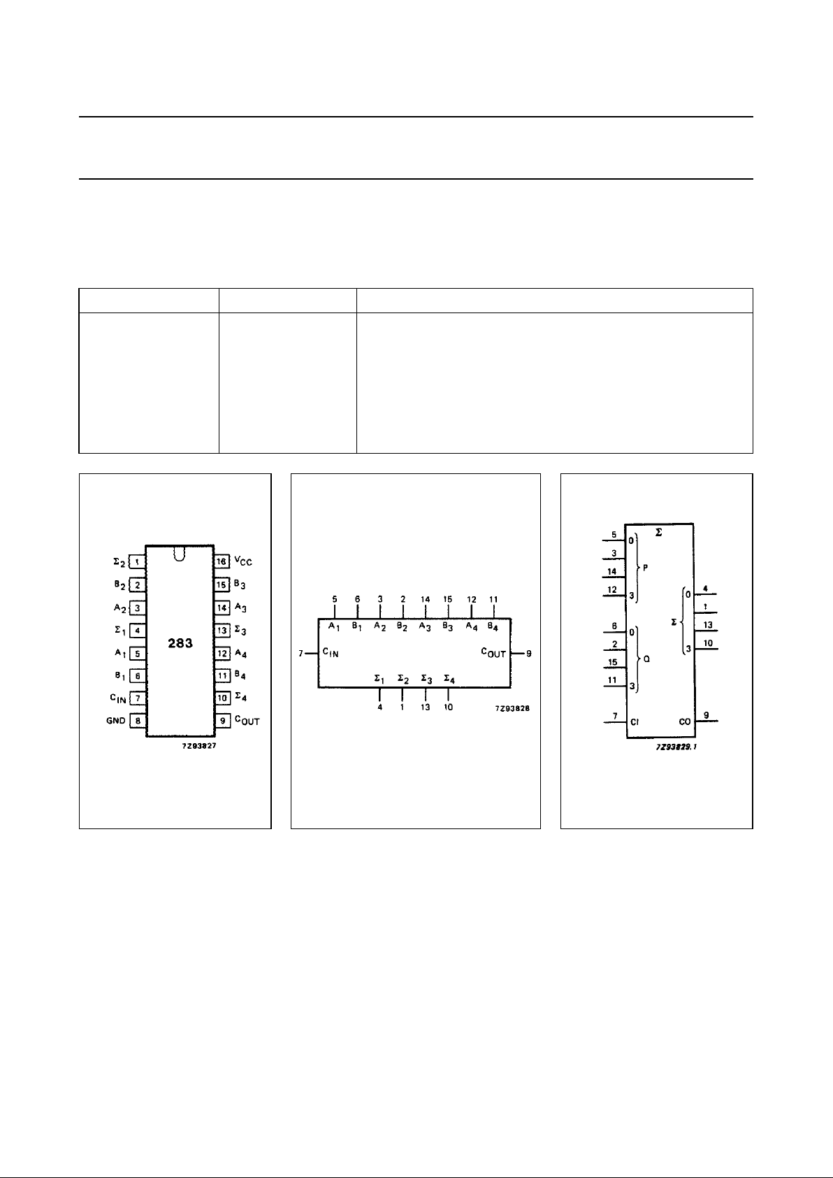
PIN NO. SYMBOL NAME AND FUNCTION
4, 1, 13, 10 ∑
1
to ∑
4
sum outputs
5, 3, 14, 12 A
1
to A
4
A operand inputs
6, 2, 15, 11 B
1
to B
4
B operand inputs
7C
IN
carry input
8 GND ground (0 V)
9C
OUT
carry output
16 V
CC
positive supply voltage
Fig.1 Pin configuration. Fig.2 Logic symbol. Fig.3 IEC logic symbol.
Page 4

December 1990 4
Philips Semiconductors Product specification
4-bit binary full adder with fast carry 74HC/HCT283
FUNCTION TABLE
Note
1. H = HIGH voltage level
L = LOW voltage level
2. example
1001
1010
----10011
3. for active HIGH, example = (9 + 10 = 19)
4. for active LOW, example = (carry + 6 + 5 = 12)
PINS CINA1A2A
3
A4B1B
2
B3B
4
∑1∑
2
∑
3
∑
4
C
OUT
EXAMPLE
(2)
logic levels L L H L H H L L H H H L L H
active HIGH 0 0 1 0 1 1 0 0 1 1 1001
(3)
active LOW 1 1 0 1 0 0 1 1 0 0 0110
(4)
Fig.4 Functional diagram.
Page 5

December 1990 5
Philips Semiconductors Product specification
4-bit binary full adder with fast carry 74HC/HCT283
Fig.5 Logic diagram.
Page 6

December 1990 6
Philips Semiconductors Product specification
4-bit binary full adder with fast carry 74HC/HCT283
DC CHARACTERISTICS FOR 74HC
For the DC characteristics see
“74HC/HCT/HCU/HCMOS Logic Family Specifications”
.
Output capability: standard
ICC category: MSI
AC CHARACTERISTICS FOR 74HC
GND = 0 V; t
r=tf
= 6 ns; CL= 50 pF
SYMBOL PARAMETER
T
amb
(°C)
UNIT
TEST CONDITIONS
74HC
V
CC
(V)
WAVEFORMS
+25 −40 to +85 −40 to +125
min. typ. max. min. max. min. max.
t
PHL
/ t
PLH
propagation delay
CIN to ∑
1
52
19
15
160
32
27
200
40
34
240
48
41
ns 2.0
4.5
6.0
Fig.6
t
PHL
/ t
PLH
propagation delay
CIN to ∑
2
58
21
17
180
36
31
225
45
38
270
54
46
ns 2.0
4.5
6.0
Fig.6
t
PHL
/ t
PLH
propagation delay
CIN to ∑
3
63
23
18
195
39
33
245
49
42
295
59
50
ns 2.0
4.5
6.0
Fig.6
t
PHL
/ t
PLH
propagation delay
CIN to ∑
4
74
27
22
230
46
39
290
58
49
345
69
59
ns 2.0
4.5
6.0
Fig.6
t
PHL
/ t
PLH
propagation delay
An or Bn to ∑
n
69
25
20
210
42
36
265
53
45
315
63
54
ns 2.0
4.5
6.0
Fig.6
t
PHL
/ t
PLH
propagation delay
CIN to C
OUT
63
23
18
195
39
33
245
49
42
295
59
50
ns 2.0
4.5
6.0
Fig.6
t
PHL
/ t
PLH
propagation delay
An or Bn to C
OUT
63
23
18
195
39
33
245
49
42
295
59
50
ns 2.0
4.5
6.0
Fig.6
t
THL
/ t
TLH
output transition time 19
7
6
75
15
13
95
19
16
110
22
19
ns 2.0
4.5
6.0
Fig.6
Page 7

December 1990 7
Philips Semiconductors Product specification
4-bit binary full adder with fast carry 74HC/HCT283
DC CHARACTERISTICS FOR 74HCT
For the DC characteristics see
“74HC/HCT/HCU/HCMOS Logic Family Specifications”
.
Output capability: standard
ICC category: MSI
Note to HCT types
The value of additional quiescent supply current (∆I
CC
) for a unit load of 1 is given in the family specifications.
To determine ∆ICC per input, multiply this value by the unit load coefficient shown in the table below.
AC CHARACTERISTICS FOR 74HCT
GND = 0 V; t
r=tf
= 6 ns; CL= 50 pF
INPUT UNIT LOAD COEFFICIENT
C
IN
B2, A2, A
1
B
1
1.50
1.00
0.40
B
4
, A4, A3, B
3
0.50
SYMBOL PARAMETER
T
amb
(°C)
UNIT
TEST CONDITIONS
74HCT
V
CC
(V)
WAVEFORMS
+25 −40 to +85 −40 to +125
min. typ. max. min. max. min. max.
t
PHL
/ t
PLH
propagation delay
CIN to ∑
1
18 31 39 47 ns 4.5 Fig.6
t
PHL
/ t
PLH
propagation delay
CIN to ∑
2
25 43 54 65 ns 4.5 Fig.6
t
PHL
/ t
PLH
propagation delay
CIN to ∑
3
27 46 58 69 ns 4.5 Fig.6
t
PHL
/ t
PLH
propagation delay
CIN to ∑
4
31 53 66 80 ns 4.5 Fig.6
t
PHL
/ t
PLH
propagation delay
An or Bn to ∑
n
29 49 61 74 ns 4.5 Fig.6
t
PHL
/ t
PLH
propagation delay
CIN to C
OUT
27 46 58 69 ns 4.5 Fig.6
t
PHL
/ t
PLH
propagation delay
An or Bn to C
OUT
28 48 60 72 ns 4.5 Fig.6
t
THL
/ t
TLH
output transition time 7 15 19 22 ns 4.5 Fig.6
Page 8

December 1990 8
Philips Semiconductors Product specification
4-bit binary full adder with fast carry 74HC/HCT283
AC WAVEFORMS
Fig.6 Waveforms showing the inputs (CIN, An, Bn)
to the outputs (∑n, C
OUT
) propagation delays
and the output transition times.
(1) HC : VM= 50%; VI= GND to VCC.
HCT: VM= 1.3 V; VI= GND to 3 V.
APPLICATION INFORMATION
Fig.7 3-bit adder.
Fig.8 2-bit and 1-bit adder.
Fig.9 5-input encoder.
Fig.10 5-input majority gate.
Notes to Figs 7 to 10
Figure 7 shows a 3-bit adder using the “283”. Tying the
operand inputs of the fourth adder (A3, B3) LOW makes ∑
3
dependent on, and equal to, the carry from the third adder.
Based on the same principle, Figure 8 shows a method of
dividing the “283” into a 2-bit and 1-bit adder. The third
stage adder (A2, B2, ∑ 2) is used simply as means of
transferring the carry into the fourth stage (via A2 and B2)
and transferring the carry from the second stage on ∑2.
Note that as long as long as A2 and B2 are the same, HIGH
or LOW, they do not influence ∑2. Similarly, when A2 and
B2 are the same, the carry into the third stage does not
influence the carry out of the third stage. Figure 9 shows a
method of implementing a 5-input encoder, where the
inputs are equally weighted. The outputs ∑
0
, ∑1 and ∑
2
produce a binary number equal to the number inputs (I1 to
I5) that are HIGH. Figure 10 shows a method of
implementing a 5-input majority gate. When three or more
inputs (I1 to I5) are HIGH, the output M5 is HIGH.
PACKAGE OUTLINES
See
“74HC/HCT/HCU/HCMOS Logic Package Outlines”
.
 Loading...