

Page 1

INTEGRATED CIRCUITS
DATA SH EET
74HC1G14; 74HCT1G14
Inverting Schmitt-trigger
Product specification
File under Integrated Circuits, IC06
1998 Aug 05
Page 2
Philips Semiconductors Product specification
Inverting Schmitt-trigger 74HC1G14; 74HCT1G14
FEATURES
• Wide operating voltage range:
2.0 to 6.0 V
• Symmetrical output impedance
• High noise immunity
• Low power dissipation
• Balanced propagation delays
• Very small 5 pins package
• Applications
– Wave and pulse shapers
– Astable multivibrators
– Monostable multivibrators
• Output capability: standard.
DESCRIPTION
The 74HC1G/HCT1G14 is a
high-speed Si-gate CMOS device.
The 74HC1G/HCT1G14 provides the
inverting buffer function with
Schmitt-trigger action. These devices
are capable of transforming slowly
changing input signals into sharply
defined, jitter-free output signals.
1
The standard output currents are
⁄
2
compared to the 74HC/HCT14.
FUNCTION TABLE
See note 1.
INPUT
inA
OUTPUT
outY
LH
HL
QUICK REFERENCE DATA
GND = 0 V; T
=25°C; tr=tf= 6.0 ns.
amb
SYMBOL PARAMETER CONDITIONS
t
PHL/tPLH
C
I
propagation
delay inA to outY
input
CL=15pF
VCC=5V
capacitance
C
PD
power
notes 1 and 2 20 22 pF
dissipation
capacitance
Notes
1. C
is used to determine the dynamic power dissipation (PDin µW).
PD
PD=CPD× V
2
× fi+ ∑ (CL× V
CC
2
× fo) where:
CC
fi= input frequency in MHz;
fo= output frequency in MHz;
CL= output load capacitance in pF;
VCC= supply voltage in V;
∑ (CL× V
2. For HC1G the condition is VI= GND to V
2
× fo) = sum of outputs.
CC
CC.
For HCT1G the condition is VI= GND to VCC− 1.5 V.
PINNING
PIN SYMBOL DESCRIPTION
1 n.c. not connected
2 inA data input
3 GND ground (0 V)
4 outY data output
5V
CC
DC supply voltage
TYP.
UNIT
HC1G HCT1G
10 15 ns
1.5 1.5 pF
Note
1. H = HIGH voltage level;
L = LOW voltage level.
1998 Aug 05 2
Page 3
Philips Semiconductors Product specification
Inverting Schmitt-trigger 74HC1G14; 74HCT1G14
ORDERING AND PACKAGE INFORMATION
OUTSIDE NORTH
PACKAGES
AMERICA
74HC1G14GW
74HCT1G14GW 5 SC-88A plastic SOT353 TF
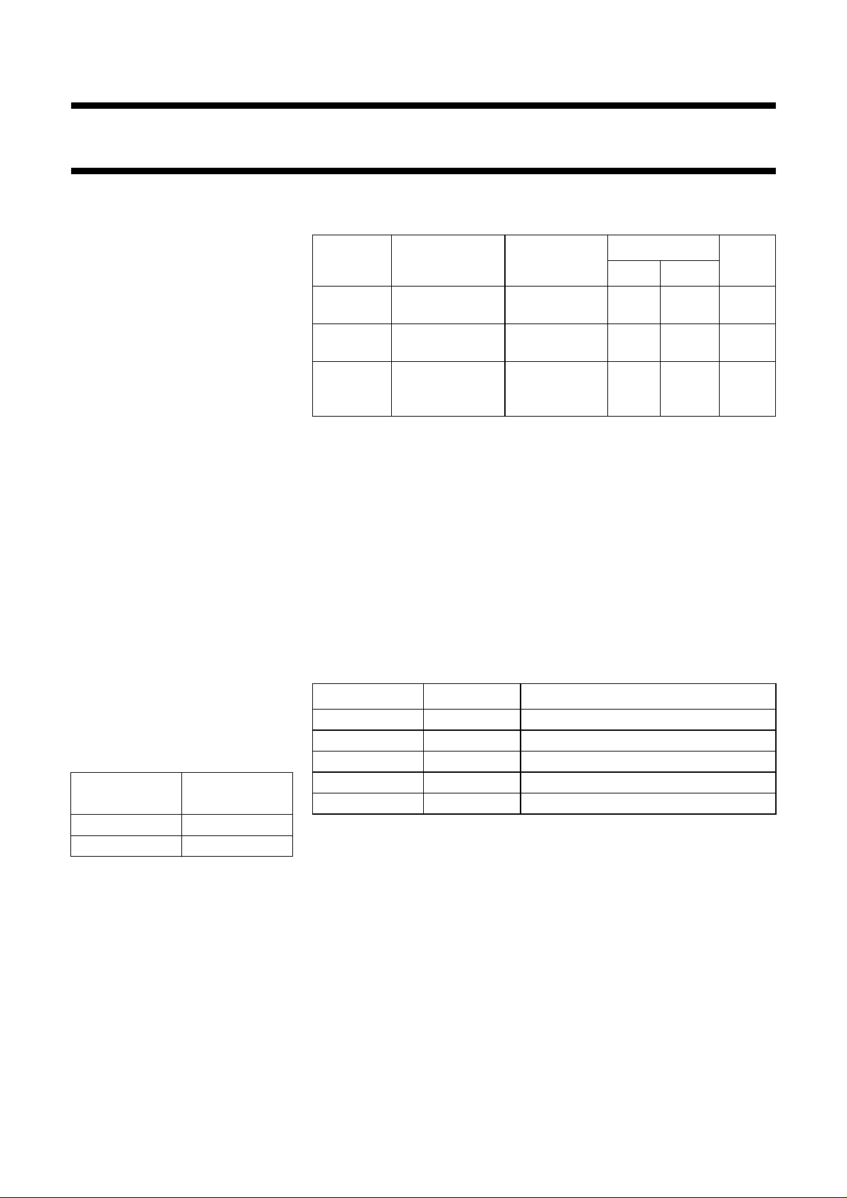
handbook, halfpage
n.c
inA
GND
TEMPERATURE
−40 to +125 °C
1
2
14
3
MNA022
RANGE
V
5
outY
4
CC
PINS PACKAGE MATERIAL CODE MARKING
5 SC-88A plastic SOT353 HF
handbook, halfpage
inA outY
2
4
MNA023
handbook, halfpage
Fig.1 Pin configuration.
24
MNA024
Fig.3 IEC logic symbol.
handbook, halfpage
inA
Fig.2 Logic symbol.
outY
MNA025
Fig.4 Logic diagram.
1998 Aug 05 3
Page 4
Philips Semiconductors Product specification
Inverting Schmitt-trigger 74HC1G14; 74HCT1G14
RECOMMENDED OPERATING CONDITIONS
SYMBOL PARAMETER
UNIT CONDITIONS
MIN. TYP. MAX. MIN. TYP. MAX.
74HC1G 74HCT1G
V
CC
V
I
V
O
T
amb
DC supply voltage 2.0 5.0 6.0 4.5 5.0 5.5 V
input voltage 0 − V
output voltage 0 − V
operating ambient
−40 +25 +125 −40 +25 +125 °C see DC and AC
0 − V
CC
0 − V
CC
CC
CC
temperature range
V
V
characteristics per device
LIMITING VALUES
In accordance with the Absolute Maximum Rating System (IEC 134); voltages are referenced to GND (ground = 0 V).
SYMBOL P ARAMETER CONDITIONS MIN. MAX. UNIT
V
CC
±I
IK
±I
OK
±I
O
DC supply voltage −0.5 +7.0 V
DC input diode current VI<−0.5 or VI> VCC+ 0.5 V; note 1 − 20 mA
DC output diode current VO<−0.5 or VO> VCC+ 0.5 V; note 1 − 20 mA
DC output source or sink
−0.5 V < VO< VCC+ 0.5 V; note 1 − 12.5 mA
current standard outputs
±I
CC
DC VCC or GND current for
note 1 − 25 mA
types with standard outputs
T
stg
P
D
storage temperature range −65 +150 °C
power dissipation per package for temperature range: −40 to +125 °C
5 pins plastic SC-88A above +55 °C derate linearly with
− 200 mW
2.5 mW/K
Note
1. The input and output voltage ratings may be exceeded if the input and output current ratings are observed.
1998 Aug 05 4
Page 5
Philips Semiconductors Product specification
Inverting Schmitt-trigger 74HC1G14; 74HCT1G14
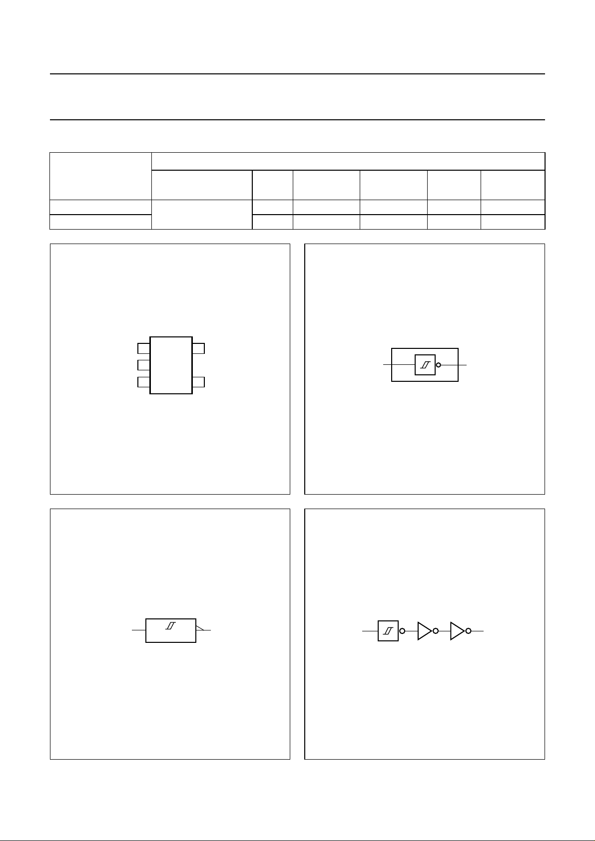
DC CHARACTERISTICS FOR THE 74HC1G
Over recommended operating conditions; voltages are referenced to GND (ground = 0 V).
T
SYMBOL PARAMETER
V
OH
HIGH-level output
voltage; all outputs
V
OH
HIGH-level output
voltage; standard
outputs
V
OL
LOW-level output
voltage; all outputs
V
OL
LOW-level output
voltage; standard
outputs
I
I
I
CC
input leakage current −− 1.0 − 1.0 µA 6.0 VI=VCCor GND
quiescent supply
current
(°C)
amb
−40 to +85 −40 to +125
MIN. TYP.
(1)
MAX. MIN. MAX.
UNIT
1.9 2.0 − 1.9 − V 2.0 VI=VIHor VIL;
4.4 4.5 − 4.4 − V 4.5
5.9 6.0 − 5.9 − V 6.0
4.13 4.32 − 3.7 − V 4.5 VI=VIHor VIL;
5.63 5.81 − 5.2 − V 6.0 V
− 0 0.1 − 0.1 V 2.0 VI=VIHor VIL;
− 0 0.1 − 0.1 V 4.5
− 0 0.1 − 0.1 V 6.0
− 0.15 0.33 − 0.4 V 4.5 VI=VIHor VIL;
− 0.16 0.33 − 0.4 V 6.0 V
−− 10 − 20 µA 6.0 VI=VCCor GND;
TEST CONDITIONS
VCC (V) OTHER
−IO=20µA
−IO= 2.0 mA
or VIL;
I=VIH
−IO= 2.6 mA
IO=20µA
IO= 2.0 mA
or VIL;
I=VIH
IO= 2.6 mA
IO=0
Note
1. All typical values are measured at T
amb
=25°C.
DC CHARACTERISTICS FOR THE 74HC1G14
Voltages are referenced to GND (ground = 0 V).
SYMBOL PARAMETER
MIN. TYP.
V
T+
positive-going threshold 0.7 1.09 1.5 0.7 1.5 V 2.0 see Figs 5 and 6
1.7 2.36 3.15 1.7 3.15 V 4.5
2.1 3.12 4.2 2.1 4.2 V 6.0
V
T−
negative-going threshold 0.3 0.60 0.9 0.3 0.9 V 2.0 see Figs 5 and 6
0.9 1.53 2.0 0.9 2.0 V 4.5
1.2 2.08 2.6 1.2 2.6 V 6.0
V
H
hysteresis (VT+− VT−) 0.2 0.48 1.0 0.2 1.0 V 2.0 see Figs 5 and 6
0.4 0.83 1.4 0.4 1.4 V 4.5
0.6 1.04 1.6 0.6 1.6 V 6.0
Note
1. All typical values are measured at T
amb
=25°C.
T
(°C)
amb
−40 to +85 −40 to +125
(1)
MAX. MIN. MAX.
TEST CONDITIONS
UNIT
VCC (V) WAVEFORMS
1998 Aug 05 5
Page 6

Philips Semiconductors Product specification
Inverting Schmitt-trigger 74HC1G14; 74HCT1G14
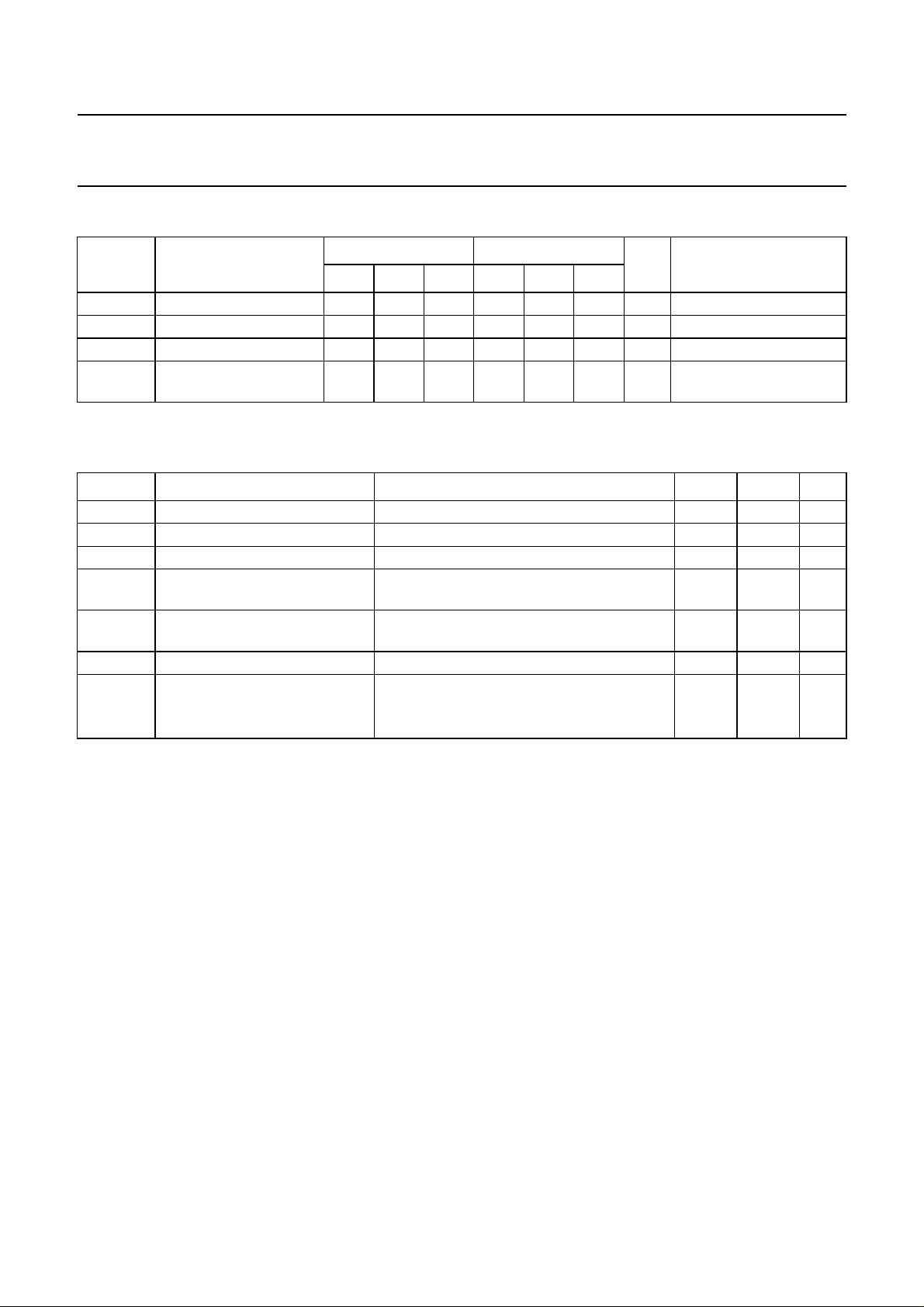
DC CHARACTERISTICS FOR THE 74HCT1G
Over recommended operating conditions; voltages are referenced to GND (ground = 0 V).
T
SYMBOL PARAMETER
V
OH
HIGH-level output
voltage; all outputs
V
OH
HIGH-level output
voltage; standard
outputs
V
OL
LOW-level output
voltage; all outputs
V
OL
LOW-level output
voltage; standard
outputs
I
I
I
CC
input leakage current −− 1.0 − 1.0 µA 5.5 VI=VCCor GND
quiescent supply
current
∆I
CC
additional supply
current per input
(°C)
amb
−40 to +85 −40 to +125
MIN. TYP.
(1)
MAX. MIN. MAX.
UNIT
4.4 4.5 − 4.4 − V 4.5 VI=VIHor VIL;
4.13 4.32 − 3.7 − V 4.5 VI=VIHor VIL;
− 0 0.1 − 0.1 V 4.5 VI=VIHor VIL;
− 0.15 0.33 − 0.4 V 4.5 VI=VIHor VIL;
−− 10.0 − 20.0 µA 5.5 VI=VCCor GND;
−− 500 − 850 µA 4.5 to 5.5 VI=VCC− 2.1 V;
TEST CONDITIONS
VCC (V) OTHER
−IO=20µA
−IO= 2.0 mA
IO=20µA
IO= 2.0 mA
IO=0
IO=0
Note
1. All typical values are measured at T
amb
=25°C.
DC CHARACTERISTICS FOR THE 74HCT1G14
Voltages are referenced to GND (ground = 0 V).
SYMBOL PARAMETER
−40 to +85 −40 to +125
MIN. TYP.
V
T+
positive-going threshold 1.2 1.55 1.9 1.2 1.9 V 4.5 see Figs 5 and 6
1.4 1.80 2.1 1.4 2.1 V 5.5
V
T−
negative-going threshold 0.5 0.76 1.2 0.5 1.2 V 4.5 see Figs 5 and 6
0.6 0.90 1.4 0.6 1.4 V 5.5
V
H
hysteresis (VT+− VT−) 0.4 0.80 − 0.4 − V 4.5 see Figs 5 and 6
0.4 0.90 − 0.4 − V 5.5
Note
1. All typical values are measured at T
amb
=25°C.
(°C)
T
amb
(1)
MAX. MIN. MAX.
TEST CONDITIONS
UNIT
VCC (V) WAVEFORMS
1998 Aug 05 6
Page 7
Philips Semiconductors Product specification
Inverting Schmitt-trigger 74HC1G14; 74HCT1G14
AC CHARACTERISTICS FOR 74HC1G14
GND = 0 V; t
SYMBOL PARAMETER
t
PHL/tPLH
Note
1. All typical values are measured at T
AC CHARACTERISTICS FOR 74HCT1G14
GND = 0 V; t
= 6.0 ns; CL=50pF.
r=tf
propagation delay
inA to outY
= 6.0 ns; CL=50pF.
r=tf
T
(°C)
amb
−40 to +85 −40 to +125
MIN. TYP.
(1)
MAX. MIN. MAX.
UNIT
TEST CONDITIONS
VCC (V) WAVEFORMS
− 25 155 − 190 ns 2.0 see Figs 12 and 13
− 12 31 − 38 ns 4.5
− 11 26 − 32 ns 6.0
=25°C.
amb
SYMBOL PARAMETER
MIN. TYP.
t
PHL/tPLH
propagation delay
− 17 43 − 51 ns 4.5 see Figs 12 and 13
inA to outY
Note
1. All typical values are measured at T
T
(°C)
amb
−40 to +85 −40 to +125
(1)
MAX. MIN. MAX.
=25°C.
amb
TEST CONDITIONS
UNIT
VCC(V) WAFEFORMS
1998 Aug 05 7
Page 8
Philips Semiconductors Product specification
Inverting Schmitt-trigger 74HC1G14; 74HCT1G14
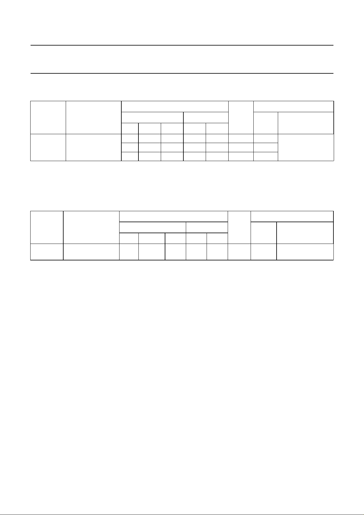
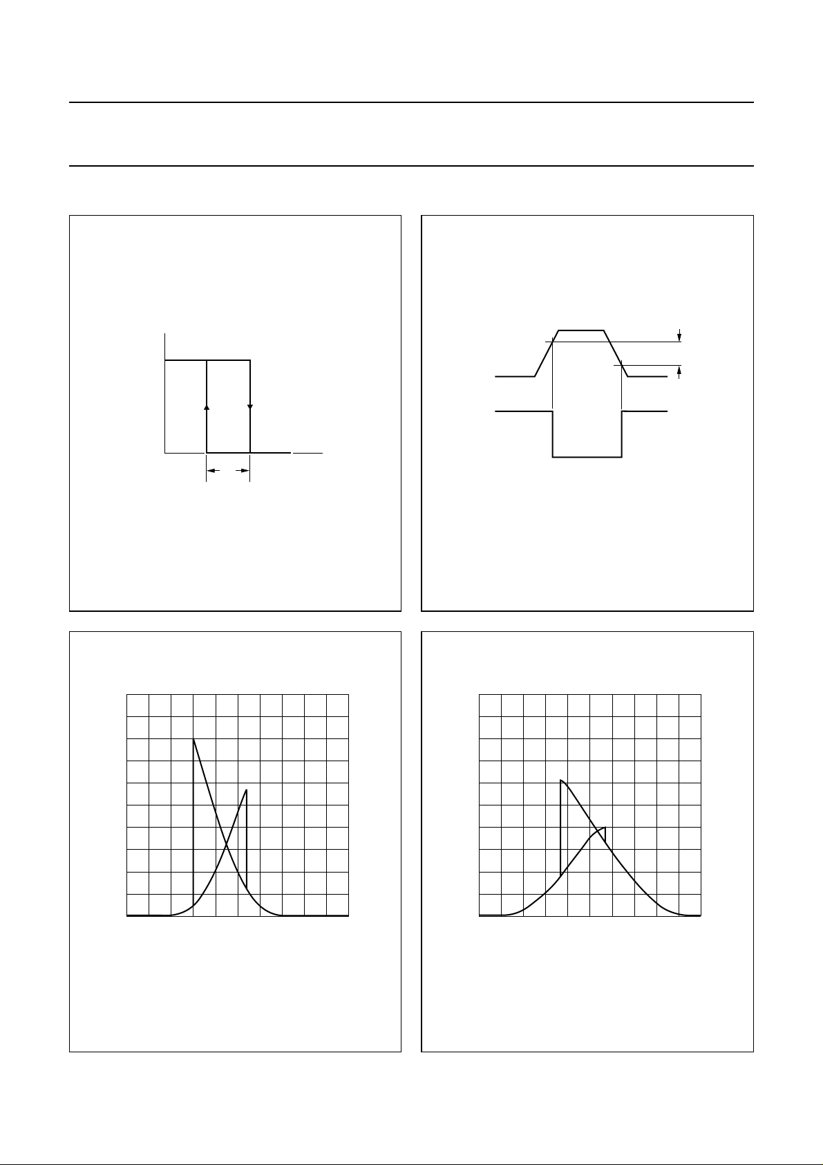
TRANSFER CHARACTERISTIC WAVEFORMS
handbook, halfpage
100
handbook, halfpage
I
CC
(µA)
V
O
V
H
V
T+
V
T−
MNA026
Fig.5 Transfer characteristic.
MNA028
handbook, halfpage
V
V
V
O
T+
I
V
T−
V
MNA027
Fig.6 The definitions of VT+, VT− and VH; where
VT+ and VT− are between limits of 20% and
70%.
1.0
handbook, halfpage
I
CC
(mA)
0.8
MNA029
H
50
0
0 2.0
1.0
VI (V)
Fig.7 Typical HC1G14 transfer characteristics;
VCC= 2.0 V.
1998 Aug 05 8
0.6
0.4
0.2
0
0 5.0
2.5
VI (V)
Fig.8 Typical HC1G14 transfer characteristics;
VCC= 4.5 V.
Page 9

Philips Semiconductors Product specification
Inverting Schmitt-trigger 74HC1G14; 74HCT1G14
1.6
handbook, halfpage
I
CC
(mA)
0.8
0
0 3.0 6.0
MNA030
VI (V)
Fig.9 Typical HC1G14 transfer characteristics;
VCC= 6.0 V.
2.0
handbook, halfpage
I
CC
(mA)
1.0
0
0 5.0
2.5
MNA031
VI (V)
Fig.10 Typical HCT1G14 transfer characteristics;
VCC= 4.5 V.
3.0
handbook, halfpage
I
CC
(mA)
2.0
1.0
0
0
3.0 6.0
MNA032
VI (V)
Fig.11 Typical HCT1G14 transfer characteristics;
VCC= 5.5 V.
1998 Aug 05 9
handbook, halfpage
inA INPUT
outY OUTPUT
(1) HC1G: VM= 50%; VI= GNDto VCC.
HCT1G: V
= 1.3V; VI= GNDto 3.0 V.
M
(1)
V
M
t
PHL
(1)
V
M
t
PLH
MNA033
Fig.12 The input (inA) to output (outY) propagation
delays.
Page 10

Philips Semiconductors Product specification
Inverting Schmitt-trigger 74HC1G14; 74HCT1G14
handbook, halfpage
V
PULSE
GENERATOR
Definitions for test circuit:
CL= load capacitance including jig and probe capacitance (See “AC characteristics for 74HC1G14”
and “AC characteristics for 74HCT1G14” for values).
= termination resistance should be equal to the output impedance Zo of the pulse generator.
R
T
I
V
CC
V
D.U.T.
R
T
O
C
L
Fig.13 Load circuitry for switching times.
50 pF
MNA034
1998 Aug 05 10
Page 11

Philips Semiconductors Product specification
Inverting Schmitt-trigger 74HC1G14; 74HCT1G14
APPLICATION INFORMATION
The slow input rise and fall times cause additional power
dissipation, this can be calculated using the following
formula:
Pad=fi×(tr× I
CCa+tf×ICCa
) × V
CC
Where:
Pad= additional power dissipation (µW)
fi= input frequency (MHz)
tr= input rise time (ns); 10% to 90%
tf= input fall time (ns); 90% to 10%
= average additional supply current (µA).
I
CCa
Average I
differs with positive or negative input
CCa
transitions, as shown in Fig.14 and Fig.15.
HC1G/HCT1G14 used in relaxation oscillator circuit,
see Fig.14 and Fig.16.
Note to the application information:
1. All values given are typical unless otherwise specified.
200
handbook, halfpage
average
I
CC
(µA)
150
positive-going
100
50
negative-going
0
0 2.0 4.0 6.0
Fig.14 Average ICC for HC1G Schmitt-trigger
devices; linear change of VI between
0.1VCCto 0.9VCC.
MNA036
edge
edge
VCC (V)
200
handbook, halfpage
average
I
CC
(µA)
150
100
50
0
0462
positive-going
negative-going
MNA058
edge
edge
V
(V)
CC
Fig.15 Average ICC for HCT1G Schmitt-trigger
devices; linear change of VI between
0.1VCCto 0.9VCC.
1998 Aug 05 11
handbook, halfpage
For HC1G:
For HCT1G:
Fig.16 Relaxation oscillator using the
1
≈=
--T
1
--T
1
-----------------------
0.8 RC×
≈=
-------------------------- -
0.67 RC×
f
f
HC1G/HCT1G14.
R
C
MNA035
1
Page 12

Philips Semiconductors Product specification
Inverting Schmitt-trigger 74HC1G14; 74HCT1G14
PACKAGE OUTLINE
Plastic surface mounted package; 5 leads SOT353
D
y
45
132
e
1
e
b
p
wBM
A
A
1
E
H
E
detail X
Q
L
p
AB
X
v M
A
c
0 1 2 mm
scale
DIMENSIONS (mm are the original dimensions)
A
UNIT
mm
A
1.1
0.8
OUTLINE
VERSION
SOT353
max
0.1
1
b
cD
p
0.30
0.20
IEC JEDEC EIAJ
0.25
0.10
2.2
1.8
(2)
E
1.35
1.3
1.15
REFERENCES
e
e
1
0.65
1998 Aug 05 12
H
2.2
2.0
L
Qywv
p
E
0.45
0.15
0.25
0.15
0.2 0.10.2
EUROPEAN
PROJECTION
ISSUE DATE
97-02-28SC-88A
Page 13

Philips Semiconductors Product specification
Inverting Schmitt-trigger 74HC1G14; 74HCT1G14
SOLDERING
Introduction
There is no soldering method that is ideal for all IC
packages. Wave soldering is often preferred when
through-hole and surface mounted components are mixed
on one printed-circuit board. However, wave soldering is
not always suitable for surface mounted ICs, or for
printed-circuits with high population densities. In these
situations reflow soldering is often used.
This text gives a very brief insight to a complex technology.
A more in-depth account of soldering ICs can be found in
our
“Data Handbook IC26; Integrated Circuit Packages”
(order code 9398 652 90011).
Reflow soldering
Reflow soldering techniques are suitable for all SO
packages.
Reflow soldering requires solder paste (a suspension of
fine solder particles, flux and binding agent) to be applied
to the printed-circuit board by screen printing, stencilling or
pressure-syringe dispensing before package placement.
Several techniques exist for reflowing; for example,
thermal conduction by heated belt. Dwell times vary
between 50 and 300 seconds depending on heating
method. Typical reflow temperatures range from
215 to 250 °C.
Preheating is necessary to dry the paste and evaporate
the binding agent. Preheating duration: 45 minutes at
45 °C.
Wave soldering
Wave soldering techniques can be used for all SO
packages if the following conditions are observed:
• A double-wave (a turbulent wave with high upward
pressure followed by a smooth laminar wave) soldering
technique should be used.
• The longitudinal axis of the package footprint must be
parallel to the solder flow.
• The package footprint must incorporate solder thieves at
the downstream end.
During placement and before soldering, the package must
be fixed with a droplet of adhesive. The adhesive can be
applied by screen printing, pin transfer or syringe
dispensing. The package can be soldered after the
adhesive is cured.
Maximum permissible solder temperature is 260 °C, and
maximum duration of package immersion in solder is
10 seconds, if cooled to less than 150 °C within
6 seconds. Typical dwell time is 4 seconds at 250 °C.
A mildly-activated flux will eliminate the need for removal
of corrosive residues in most applications.
Repairing soldered joints
Fix the component by first soldering two diagonallyopposite end leads. Use only a low voltage soldering iron
(less than 24 V) applied to the flat part of the lead. Contact
time must be limited to 10 seconds at up to 300 °C. When
using a dedicated tool, all other leads can be soldered in
one operation within 2 to 5 seconds between
270 and 320 °C.
1998 Aug 05 13
Page 14

Philips Semiconductors Product specification
Inverting Schmitt-trigger 74HC1G14; 74HCT1G14
DEFINITIONS
Data sheet status
Objective specification This data sheet contains target or goal specifications for product development.
Preliminary specification This data sheet contains preliminary data; supplementary data may be published later.
Product specification This data sheet contains final product specifications.
Limiting values
Limiting values given are in accordance with the Absolute Maximum Rating System (IEC 134). Stress above one or
more of the limiting values may cause permanent damage to the device. These are stress ratings only and operation
of the device at these or at any other conditions above those given in the Characteristics sections of the specification
is not implied. Exposure to limiting values for extended periods may affect device reliability.
Application information
Where application information is given, it is advisory and does not form part of the specification.
LIFE SUPPORT APPLICATIONS
These products are not designed for use in life support appliances, devices, or systems where malfunction of these
products can reasonably be expected to result in personal injury. Philips customers using or selling these products for
use in such applications do so at their own risk and agree to fully indemnify Philips for any damages resulting from such
improper use or sale.
1998 Aug 05 14
Page 15

Philips Semiconductors Product specification
Inverting Schmitt-trigger 74HC1G14; 74HCT1G14
NOTES
1998 Aug 05 15
Page 16

Philips Semiconductors – a worldwide company
Argentina: see South America
Australia: 34 Waterloo Road, NORTH RYDE, NSW 2113,
Tel. +61 2 9805 4455, Fax. +61 2 9805 4466
Austria: Computerstr. 6, A-1101 WIEN, P.O. Box 213, Tel. +43 160 1010,
Fax. +43 160 101 1210
Belarus: Hotel Minsk Business Center, Bld. 3, r. 1211, Volodarski Str. 6,
220050 MINSK, Tel. +375 172 200 733, Fax. +375 172 200 773
Belgium: see The Netherlands
Brazil: see South America
Bulgaria: Philips Bulgaria Ltd., Energoproject, 15th floor,
51 James Bourchier Blvd., 1407 SOFIA,
Tel. +359 2 689 211, Fax. +359 2 689 102
Canada: PHILIPS SEMICONDUCTORS/COMPONENTS,
Tel. +1 800 234 7381
China/Hong Kong: 501 Hong Kong Industrial Technology Centre,
72 Tat Chee Avenue, Kowloon Tong, HONG KONG,
Tel. +852 2319 7888, Fax. +852 2319 7700
Colombia: see South America
Czech Republic: see Austria
Denmark: Prags Boulevard 80, PB 1919, DK-2300 COPENHAGEN S,
Tel. +45 32 88 2636, Fax. +45 31 57 0044
Finland: Sinikalliontie 3, FIN-02630 ESPOO,
Tel. +358 9 615800, Fax. +358 9 61580920
France: 51 Rue Carnot, BP317, 92156 SURESNES Cedex,
Tel. +33 1 40 99 6161, Fax. +33 1 40 99 6427
Germany: Hammerbrookstraße 69, D-20097 HAMBURG,
Tel. +49 40 23 53 60, Fax. +49 40 23 536 300
Greece: No. 15, 25th March Street, GR 17778 TAVROS/ATHENS,
Tel. +30 1 4894 339/239, Fax. +30 1 4814 240
Hungary: see Austria
India: Philips INDIA Ltd, Band Box Building, 2nd floor,
254-D, Dr. Annie Besant Road, Worli, MUMBAI 400 025,
Tel. +91 22 493 8541, Fax. +91 22 493 0966
Indonesia: PT Philips Development Corporation, Semiconductors Division,
Gedung Philips, Jl. Buncit Raya Kav.99-100, JAKARTA 12510,
Tel. +62 21 794 0040 ext. 2501, Fax. +62 21 794 0080
Ireland: Newstead, Clonskeagh, DUBLIN 14,
Tel. +353 1 7640 000, Fax. +353 1 7640 200
Israel: RAPAC Electronics, 7 Kehilat Saloniki St, PO Box 18053,
TEL AVIV 61180, Tel. +972 3 645 0444, Fax. +972 3 649 1007
Italy: PHILIPS SEMICONDUCTORS, Piazza IV Novembre 3,
20124 MILANO, Tel. +39 2 6752 2531, Fax. +39 2 6752 2557
Japan: Philips Bldg 13-37, Kohnan 2-chome, Minato-ku,
TOKYO 108-8507, Tel. +81 3 3740 5130, Fax. +81 3 3740 5077
Korea: Philips House, 260-199 Itaewon-dong, Yongsan-ku, SEOUL,
Tel. +82 2 709 1412, Fax. +82 2 709 1415
Malaysia: No. 76 Jalan Universiti, 46200 PETALING JAYA, SELANGOR,
Tel. +60 3 750 5214, Fax. +60 3 757 4880
Mexico: 5900 Gateway East, Suite 200, EL PASO, TEXAS 79905,
Tel. +9-5 800 234 7381
Middle East: see Italy
Netherlands: Postbus 90050, 5600 PB EINDHOVEN, Bldg. VB,
Tel. +31 40 27 82785, Fax. +31 40 27 88399
New Zealand: 2 Wagener Place, C.P.O. Box 1041, AUCKLAND,
Tel. +64 9 849 4160, Fax. +64 9 849 7811
Norway: Box 1, Manglerud 0612, OSLO,
Tel. +47 22 74 8000, Fax. +47 22 74 8341
Pakistan: see Singapore
Philippines: Philips Semiconductors Philippines Inc.,
106 Valero St. Salcedo Village, P.O. Box 2108 MCC, MAKATI,
Metro MANILA, Tel. +63 2 816 6380, Fax. +63 2 817 3474
Poland: Ul. Lukiska 10, PL 04-123 WARSZAWA,
Tel. +48 22 612 2831, Fax. +48 22 612 2327
Portugal: see Spain
Romania: see Italy
Russia: Philips Russia, Ul. Usatcheva 35A, 119048 MOSCOW,
Tel. +7 095 755 6918, Fax. +7 095 755 6919
Singapore: Lorong 1, Toa Payoh, SINGAPORE 319762,
Tel. +65 350 2538, Fax. +65 251 6500
Slovakia: see Austria
Slovenia: see Italy
South Africa: S.A. PHILIPS Pty Ltd., 195-215 Main Road Martindale,
2092 JOHANNESBURG, P.O. Box 7430 Johannesburg 2000,
Tel. +27 11 470 5911, Fax. +27 11 470 5494
South America: Al. Vicente Pinzon, 173, 6th floor,
04547-130 SÃO PAULO, SP, Brazil,
Tel. +55 11 821 2333, Fax. +55 11 821 2382
Spain: Balmes 22, 08007 BARCELONA,
Tel. +34 93 301 6312, Fax. +34 93 301 4107
Sweden: Kottbygatan 7, Akalla, S-16485 STOCKHOLM,
Tel. +46 8 5985 2000, Fax. +46 8 5985 2745
Switzerland: Allmendstrasse 140, CH-8027 ZÜRICH,
Tel. +41 1 488 2741 Fax. +41 1 488 3263
Taiwan: Philips Semiconductors, 6F, No. 96, Chien Kuo N. Rd., Sec. 1,
TAIPEI, Taiwan Tel. +886 2 2134 2865, Fax. +886 2 2134 2874
Thailand: PHILIPS ELECTRONICS (THAILAND) Ltd.,
209/2 Sanpavuth-Bangna Road Prakanong, BANGKOK 10260,
Tel. +66 2 745 4090, Fax. +66 2 398 0793
Turkey: Talatpasa Cad. No. 5, 80640 GÜLTEPE/ISTANBUL,
Tel. +90 212 279 2770, Fax. +90 212 282 6707
Ukraine: PHILIPS UKRAINE, 4 Patrice Lumumba str., Building B, Floor 7,
252042 KIEV, Tel. +380 44 264 2776, Fax. +380 44 268 0461
United Kingdom: Philips Semiconductors Ltd., 276 Bath Road, Hayes,
MIDDLESEX UB3 5BX, Tel. +44 181 730 5000, Fax. +44 181 754 8421
United States: 811 East Arques Avenue, SUNNYVALE, CA 94088-3409,
Tel. +1 800 234 7381
Uruguay: see South America
Vietnam: see Singapore
Yugoslavia: PHILIPS, Trg N. Pasica 5/v, 11000 BEOGRAD,
Tel. +381 11 625 344, Fax.+381 11 635 777
For all other countries apply to: Philips Semiconductors,
International Marketing & Sales Communications, Building BE-p, P.O. Box 218,
5600 MD EINDHOVEN, The Netherlands, Fax. +31 40 27 24825
© Philips Electronics N.V. 1998 SCA60
All rights are reserved. Reproduction in whole or in part is prohibited without the prior written consent of the copyright owner.
The information presented in this document does not form part of any quotation or contract, is believed to be accurate and reliable and may be changed
without notice. No liability will be accepted by the publisher for any consequence of its use. Publication thereof does not convey nor imply any license
under patent- or other industrial or intellectual property rights.
Internet: http://www.semiconductors.philips.com
Printed in The Netherlands 245106/00/01/pp16 Date of release: 1998 Aug 05 Document order number: 9397750 03652
 Loading...