

Page 1
DATA SH EET
Product specification
Supersedes data of September 1993
File under Integrated Circuits, IC06
1998 Jun 10
INTEGRATED CIRCUITS
74HC/HCT181
4-bit arithmetic logic unit
For a complete data sheet, please also download:
•The IC06 74HC/HCT/HCU/HCMOS Logic Family Specifications
•The IC06 74HC/HCT/HCU/HCMOS Logic Package Information
•The IC06 74HC/HCT/HCU/HCMOS Logic Package Outlines
Page 2

1998 Jun 10 2
Philips Semiconductors Product specification
4-bit arithmetic logic unit 74HC/HCT181
FEATURES
• Full carry look-ahead for high-speed arithmetic
operation on long words
• Provides 16 arithmetic operations: add, subtract,
compare, double, plus 12 others
• Provides all 16 logic operations of two variables:
EXCLUSIVE-OR, compare, AND, NAND, NOR, OR plus
10 other logic operations
• Output capability: standard,
A=B open drain
• I
CC
category: MSI
GENERAL DESCRIPTION
The 74HC/HCT181 are high-speed Si-gate CMOS devices
and are pin compatible with low power Schottky TTL
(LSTTL). They are specified in compliance with JEDEC
standard no. 7A.
The 74HC/HCT181 are 4-bit high-speed parallel
Arithmetic Logic Units (ALU). Controlled by the four
function select inputs (S
0
to S3) and the mode control input
(M), they can perform all the 16 possible logic operations
or 16 different arithmetic operations on active HIGH or
active LOW operands (see function table).
When the mode control input (M) is HIGH, all internal
carries are inhibited and the device3 performs logic
operations on the individual bits as listed. When M is LOW,
the carries are enabled and the “181” performs arithmetic
operations on the two 4-bit words. The “181” incorporates
full internal carry look-ahead and provides for either ripple
carry between devices using the C
n+4
output, or for carry
look-ahead between packages using the carry
propagation (P) and carry generate (G) signals. P and
G are not affected by carry in.
When speed requirements are not stringent, it can be used
in a simple ripple carry mode by connecting the carry
output (C
n+4
) signal to the carry input (Cn) of the next unit.
For high-speed operation the device is used in conjunction
with the “182” carry look-ahead circuit. One carry
look-ahead package is required for each group of four
“181” devices. Carry look-ahead can be provided at
various levels and offers high-speed capability over
extremely long word lengths.
The comparator output (A=B) of the device goes HIGH
when all four function outputs (F0to F3) are HIGH and can
be used to indicate logic equivalence over 4 bits when the
unit is in the subtract mode. A=B is an open collector
output and can be wired-AND with other A=B outputs to
give a comparison for more than 4 bits. The open drain
output A=B should be used with an external pull-up
resistor in order to establish a logic HIGH level. The A=B
signal can also be used with the C
n+4
signal to indicate
A > B and A < B.
The function table lists the arithmetic operations that are
performed without a carry in. An incoming carry adds a one
to each operation. Thus, select code LHHL generates
A minus B minus 1 (2s complement notation) without a
carry in and generates A minus B when a carry is applied.
Because subtraction is actually performed by
complementary addition (1s complement), a carry out
means borrow; thus, a carry is generated when there is no
under-flow and no carry is generated when there is
underflow.
As indicated, the “181” can be used with either active LOW
inputs producing active LOW outputs or with active HIGH
inputs producing active HIGH outputs.
For either case the table lists the operations that are
performed to the operands.
ORDERING INFORMATION
TYPE
NUMBER
PACKAGE
NAME DESCRIPTION VERSION
74HC181N3;
74HCT181N3
DIP24 plastic dual in-line package; 24 leads (300 mil) SOT222-1
74HC181N;
74HCT181N
DIP24 plastic dual in-line package; 24 leads (600 mil) SOT101-1
74HC181D;
74HCT181D
SO24 plastic small outline package; 24 leads; body width 7.5 mm SOT137-1
Page 3
1998 Jun 10 3
Philips Semiconductors Product specification
4-bit arithmetic logic unit 74HC/HCT181
QUICK REFERENCE DATA
GND = 0 V; T
amb
=25°C; tr=tf=6ns
Notes
1. C
PD
is used to determine the dynamic power dissipation (PDin µW):
PD=CPD× V
CC
2
× fi+ ∑ (CL× V
CC
2
× fo) where:
fi= input frequency in MHz
fo= output frequency in MHz
∑ (CL× V
CC
2
× fo) = sum of outputs
CL= output load capacitance in pF
VCC= supply voltage in V
2. For HC the condition is VI= GND to V
CC
For HCT the condition is VI= GND to VCC− 1.5 V
SYMBOL PARAMETER CONDITIONS
TYPICAL
UNIT
HC HCT
t
PHL
/ t
PLH
propagation delay CL= 15 pF; VCC=5V
An or Bn to A=B 28 30 ns
C
n
to Cn+41721ns
C
I
input capacitance 3.5 3.5 pF
C
PD
power dissipation capacitance
per L package
notes 1 and 2 90 92 pF
Fig.1 Pin configuration. Fig.2 Logic symbol. Fig.3 IEC logic symbol.
A B
Page 4
1998 Jun 10 4
Philips Semiconductors Product specification
4-bit arithmetic logic unit 74HC/HCT181
PIN DESCRIPTION
PIN NO. SYMBOL NAME AND FUNCTION
1, 22, 20, 18
B0to B
3
operand inputs (active LOW)
2, 23, 21, 19
A0to A
3
operand inputs (active LOW)
6, 5, 4, 3 S
0
to S
3
select inputs
7C
n
carry input
8 M mode control input
9, 10, 11, 13
F0to F
3
function outputs (active LOW)
12 GND ground (0 V)
14 A=B comparator output
15
P carry propagate output (active LOW)
16 C
n+4
carry output
17
G carry generate output (active LOW)
24 V
CC
positive supply voltage
Fig.4 Functional diagram.
k, halfpage
MBK219
A
0
A
1
A
2
2
23
21
19
1
22
20
18 15
17
14
16
13
11
10
9
A
3
B
0
B
1
C
n+4
F
3
F
2
F
1
F
0
A=B
G
B
2
P
B
3
7
C
n
6
S
0
5
S
1
4
S
2
3
S
3
8M
Fig.5 Active HIGH operands - active LOW operands.
Page 5
1998 Jun 10 5
Philips Semiconductors Product specification
4-bit arithmetic logic unit 74HC/HCT181
FUNCTION TABLES
Notes to the function tables
1. Each bit is shifted to the next more significant position.
2. Arithmetic operations expressed in 2s complement
notation.
H = HIGH voltage level
L = LOW voltage level
MODE SELECT
INPUTS
ACTIVE HIGH INPUTS AND
OUTPUTS
S3S2S1S
0
LOGIC
(M=H)
ARITHMETIC
(2)
(M=L; Cn=H)
L
L
L
L
L
L
L
L
L
L
H
H
L
H
L
H
A
A + B
AB
logical 0
A
A+B
A+B
minus 1
L
L
L
L
H
H
H
H
L
L
H
H
L
H
L
H
AB
B
A ⊕ B
AB
A plus AB
(A + B) plus AB
A minus B minus 1
AB minus 1
H
H
H
H
L
L
L
L
L
L
H
H
L
H
L
H
A+B
A⊕B
B
AB
A plus AB
A plus B
(A + B) plus AB
AB minus 1
H
H
H
H
H
H
H
H
L
L
H
H
L
H
L
H
logical 1
A+
B
A+B
A
A plus A
(1)
(A + B) plus A
(A + B) plus A
A minus 1
Notes to the function tables
1. Each bit is shifted to the next more significant position.
2. Arithmetic operations expressed in 2s complement
notation.
H = HIGH voltage level
L = LOW voltage level
MODE SELECT
INPUTS
ACTIVE LOW INPUTS AND
OUTPUTS
S
3
S2S1S
0
LOGIC
(M=H)
ARITHMETIC
(2)
(M=L; Cn=L)
L
L
L
L
L
L
L
L
L
L
H
H
L
H
L
H
A
AB
A+B
logical 1
A minus 1
AB minus 1
AB minus 1
minus 1
L
L
L
L
H
H
H
H
L
L
H
H
L
H
L
H
A + B
B
A ⊕ B
A+B
A plus (A + B)
AB plus (A + B)
A minus B minus 1
A+B
H
H
H
H
L
L
L
L
L
L
H
H
L
H
L
H
AB
A ⊕ B
B
A + B
A plus (A + B)
A plus B
AB plus (A + B)
A+B
H
H
H
H
H
H
H
H
L
L
H
H
L
H
L
H
logical 0
A
B
AB
A
A plus A
(1)
AB plus A
AB plus A
A
Page 6
1998 Jun 10 6
Philips Semiconductors Product specification
4-bit arithmetic logic unit 74HC/HCT181
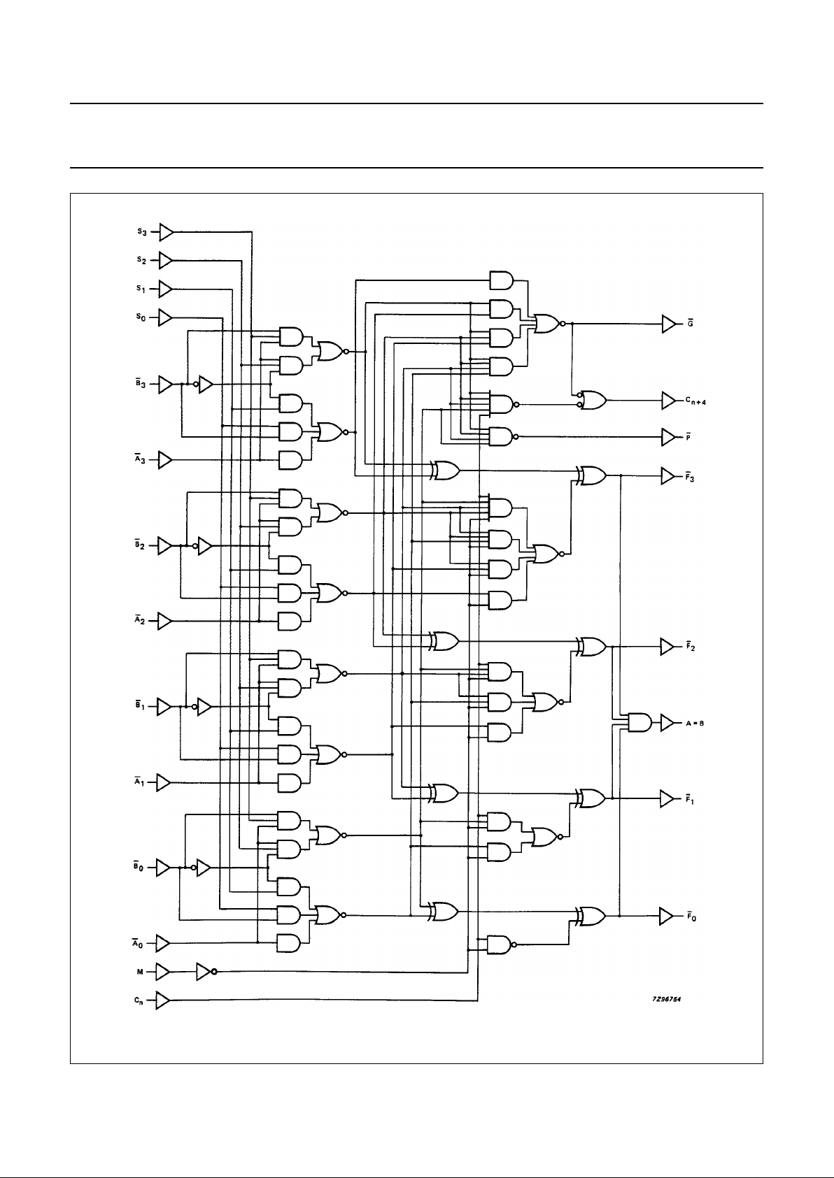
Fig.6 Logic diagram.
Page 7

1998 Jun 10 7
Philips Semiconductors Product specification
4-bit arithmetic logic unit 74HC/HCT181
Table 1 SUM MODE TEST
Function inputs S
0=S3
= 4.5 V, M = S1=S2=0V
Table 2 DIFFERENTIAL MODE TEST
Function inputs S
1=S2
= 4.5 V, M = S0=S3=0V
Table 3 LOGIC MODE TEST
Function inputs M = S
1=S2
= 4.5 V, S0=S3=0V
PARAMETER
INPUT
UNDER
TEST
OTHER INPUT, SAME BIT OTHER DATA INPUTS OUTPUT
UNDER
TEST
Apply 4.5 V Apply GND Apply 4.5 V Apply GND
t
PLH
/ t
PHL
A
i
B
i
none remaining A and BC
n
F
i
t
PLH
/ t
PHL
B
i
A
i
none remaining A and BC
n
F
i
t
PLH
/ t
PHL
A
i
B
i
none none remaining A and B, CnP
t
PLH
/ t
PHL
B
i
A
i
none none remaining A and B, CnP
t
PLH
/ t
PHL
A
i
none B
i
remaining B remaining A, C
n
G
t
PLH
/ t
PHL
B
i
none A
i
remaining B remaining A, C
n
G
t
PLH
/ t
PHL
A
i
none B
i
remaining B remaining A, C
n
C
n+4
t
PLH
/ t
PHL
B
i
none A
i
remaining B remaining A, C
n
C
n+4
t
PLH
/ t
PHL
C
n
none none all A all B any F or C
n+4
PARAMETER
INPUT
UNDER
TEST
OTHER INPUT, SAME BIT OTHER DATA INPUTS OUTPUT
UNDER
TEST
Apply 4.5 V Apply GND Apply 4.5 V Apply GND
t
PLH
/ t
PHL
A
i
none B
i
remaining A remaining B, C
n
F
i
t
PLH
/ t
PHL
B
i
A
i
none remaining A remaining B, C
n
F
i
t
PLH
/ t
PHL
A
i
none B
i
none remaining A and B, CnP
t
PLH
/ t
PHL
B
i
A
i
none none remaining A and B, CnP
t
PLH
/ t
PHL
A
i
B
i
none none remaining A and B, CnG
t
PLH
/ t
PHL
B
i
none A
i
none remaining A and B, CnG
t
PLZ
/ t
PZL
A
i
none B
i
remaining A remaining B, C
n
A=B
t
PLZ
/ t
PZL
B
i
A
i
none remaining A remaining B, C
n
A=B
t
PLH
/ t
PHL
A
i
B
i
none none remaining A and B, CnC
n+4
t
PLH
/ t
PHL
B
i
none A
i
none remaining A and B, CnC
n+4
t
PLH
/ t
PHL
C
n
none none all A and B none any F or C
n+4
PARAMETER
INPUT
UNDER
TEST
OTHER INPUT, SAME BIT OTHER DATA INPUTS OUTPUT
UNDER
TEST
Apply 4.5 V Apply GND Apply 4.5 V Apply GND
t
PLH
/ t
PHL
A
i
B
i
none none remaining A and B, CnF
i
t
PLH
/ t
PHL
B
i
A
i
none none remaining A and B, CnF
i
Page 8

1998 Jun 10 8
Philips Semiconductors Product specification
4-bit arithmetic logic unit 74HC/HCT181
RATINGS (for A=B output only)
Limiting values in accordance with the Absolute Maximum System (IEC 134)
Voltage are referenced to GND (ground = 0 V)
DC CHARACTERISTICS FOR 74HC
For the DC characteristics see
“74HC/HCT/HCU/HCMOS Logic Family Specifications”
.
Output capability: standard
ICCcategory: MSI
Voltages are referenced to GND (ground = 0 V)
Note to the DC characteristics
1. The maximum operating output voltage (V
O(max)
) is 6.0 V.
SYMBOL PARAMETER MIN. MAX. UNIT CONDITIONS
V
O
DC output voltage −0.5 +7.0 V
−I
OK
DC output diode current 20 mA for VO<−0.5 V
−I
O
DC output source or sink current 25 mA for −0.5 V < V
O
SYMBOL PARAMETER
T
amb
(°C)
UNIT
TEST CONDITIONS
74HC
V
CC
(V)
V
IL
OTHER
+25 −40 to +85 −40 to +125
min. typ. max. min. max. min. max.
I
OZ
HIGH level output
leakage current
0.5 5.0 10.0 µA
2.0
to
6.0
V
IL
note 1
VO=0or6V
Page 9

1998 Jun 10 9
Philips Semiconductors Product specification
4-bit arithmetic logic unit 74HC/HCT181
AC CHARACTERISTICS FOR 74HC
GND = 0 V; t
r=tf
= 6 ns; CL= 50 pF
SYMBOL PARAMETER
T
amb
(°C)
UNIT
TEST CONDITIONS
74HC
V
CC
(V)
MODE OTHER
+25 −40 to +85 −40 to +125
min. typ. max. min. max. min. max.
t
PHL
/ t
PLH
propagation delay
Cnto C
n+4
55
20
16
165
33
28
205
41
35
250
50
43
ns 2.0
4.5
6.0
sum
diff
M=0V;
Fig.9;
Tables 1 and 2
t
PHL
/ t
PLH
propagation delay
Cnto F
n
69
25
20
200
40
34
250
50
43
300
60
51
ns 2.0
4.5
6.0
sum
diff
M=0V;
Fig.9;
Tables 1 and 2
t
PHL
/ t
PLH
propagation delay
Anto G
72
26
21
210
42
36
265
53
45
315
63
54
ns 2.0
4.5
6.0
sum
M=S1=S2=0V;
S0=S3= 4.5 V;
Fig.7; Table 1
t
PHL
/ t
PLH
propagation delay
Bnto G
77
28
22
230
46
39
290
58
49
345
69
59
ns 2.0
4.5
6.0
sum
M=S1=S2=0V;
S0=S3= 4.5 V;
Fig.7; Table 1
t
PHL
/ t
PLH
propagation delay
Anto G
76
26
21
215
43
37
270
54
46
320
65
55
ns 2.0
4.5
6.0
diff
M=S0=S3=0V;
S1=S2= 4.5 V;
Fig.8; Table 2
t
PHL
/ t
PLH
propagation delay
Bnto G
77
28
22
240
48
41
300
60
51
360
72
61
ns 2.0
4.5
6.0
diff
M=S0=S3=0V;
S1=S2= 4.5 V;
Fig.8; Table 2
t
PHL
/ t
PLH
propagation delay
Anto P
61
22
18
185
37
31
230
46
39
280
56
48
ns 2.0
4.5
6.0
sum
M=S1=S2=0V;
S0=S3= 4.5 V;
Fig.7; Table 1
t
PHL
/ t
PLH
propagation delay
Bnto P
63
23
18
195
39
33
245
49
42
295
59
50
ns 2.0
4.5
6.0
sum
M=S1=S2=0V;
S0=S3= 4.5 V;
Fig.7; Table 1
t
PHL
/ t
PLH
propagation delay
Anto P
55
20
16
170
34
29
215
43
37
255
51
43
ns 2.0
4.5
6.0
diff
M=S0=S3=0V;
S1=S2= 4.5 V;
Fig.8; Table 2
t
PHL
/ t
PLH
propagation delay
Bnto P
63
23
18
195
39
33
245
49
42
295
59
50
ns 2.0
4.5
6.0
diff
M=S0=S3=0V;
S1=S2= 4.5 V;
Fig.8; Table 2
t
PHL
/ t
PLH
propagation delay
Aito F
i
77
28
22
230
46
39
290
58
49
345
69
59
ns 2.0
4.5
6.0
sum
M=S1=S2=0V;
S0=S3= 4.5 V;
Fig.7; Table 1
t
PHL
/ t
PLH
propagation delay
Bito F
i
85
31
25
255
51
43
320
64
54
385
77
65
ns 2.0
4.5
6.0
sum
M=S1=S2=0V;
S0=S3= 4.5 V;
Fig.7; Table 1
t
PHL
/ t
PLH
propagation delay
Aito F
i
77
28
22
235
47
40
295
59
50
355
71
60
ns 2.0
4.5
6.0
diff
M=S0=S3=0V;
S1=S2= 4.5 V;
Fig.8; Table 2
t
PHL
/ t
PLH
propagation delay
Bito F
i
83
31
24
255
51
43
320
64
54
385
77
65
ns 2.0
4.5
6.0
diff
M=S0=S3=0V;
S1=S2= 4.5 V;
Fig.8; Table 2
Page 10

1998 Jun 10 10
Philips Semiconductors Product specification
4-bit arithmetic logic unit 74HC/HCT181
Note to the AC characteristics
1. For the open drain output (A=B) only t
THL
is valid.
t
PHL
/ t
PLH
propagation delay
Aito F
i
74
27
22
230
46
39
290
58
49
345
69
59
ns 2.0
4.5
6.0
logic
M = 4.5 V;
Fig.8;
Table 3
t
PHL
/ t
PLH
propagation delay
Bito F
i
83
30
24
255
51
43
320
64
54
385
77
65
ns 2.0
4.5
6.0
logic
M = 4.5 V;
Fig.8;
Table 3
t
PHL
/ t
PLH
propagation delay
Anto C
n+4
80
29
23
235
47
40
295
59
50
355
71
60
ns 2.0
4.5
6.0
sum
M=S1=S2=0V;
S0=S3= 4.5 V;
Fig.8; Table 1
t
PHL
/ t
PLH
propagation delay
Bnto C
n+4
80
29
23
235
47
40
295
59
50
355
71
60
ns 2.0
4.5
6.0
sum
M=S1=S2=0V;
S0=S3= 4.5 V;
Fig.8; Table 1
t
PHL
/ t
PLH
propagation delay
Anto C
n+4
77
28
22
235
47
40
295
59
50
355
71
60
ns 2.0
4.5
6.0
diff
M=S0=S3=0V;
S1=S2= 4.5 V;
Fig.10; Table 2
t
PHL
/ t
PLH
propagation delay
Bnto C
n+4
85
31
25
255
51
43
320
64
54
385
77
65
ns 2.0
4.5
6.0
diff
M=S0=S3=0V;
S1=S2= 4.5 V;
Fig.10; Table 2
t
PZL
/ t
PLZ
propagation delay
Anto A=B
80
29
23
245
49
42
305
61
52
370
74
63
ns 2.0
4.5
6.0
diff
M=S0=S3=0V;
S1=S2= 4.5 V;
Fig.11; Table 2
t
PZL
/ t
PLZ
propagation delay
Bnto A=B
88
32
26
270
54
46
340
68
58
405
81
69
ns 2.0
4.5
6.0
diff
M=S0=S3=0V;
S1=S2= 4.5 V;
Fig.11; Table 2
t
PHL
/ t
PLH
propagation delay
Anto F
n
83
30
24
255
51
43
320
64
54
385
77
65
ns 2.0
4.5
6.0
sum
M=S1=S2=0V;
S0=S3= 4.5 V;
Fig.7; Table 1
t
PHL
/ t
PLH
propagation delay
Bnto F
n
85
31
25
265
53
45
330
66
56
400
80
68
ns 2.0
4.5
6.0
sum
M=S1=S2=0V;
S0=S3= 4.5 V;
Fig.7; Table 1
t
PHL
/ t
PLH
propagation delay
Anto F
n
77
28
22
240
48
41
300
60
51
360
72
61
ns 2.0
4.5
6.0
diff
M=S0=S3=0V;
S1=S2= 4.5 V;
Fig.8; Table 2
t
PHL
/ t
PLH
propagation delay
Bnto F
n
88
32
26
275
55
47
345
69
59
415
83
71
ns 2.0
4.5
6.0
diff
M=S0=S3=0V;
S1=S2= 4.5 V;
Fig.8; Table 2
t
THL
/ t
TLH
output transition
time
19
7
6
75
15
13
95
19
16
110
22
19
ns 2.0
4.5
6.0
note ;
Figs 7 and 11
SYMBOL PARAMETER
T
amb
(°C)
UNIT
TEST CONDITIONS
74HC
V
CC
(V)
MODE OTHER
+25 −40 to +85 −40 to +125
min. typ. max. min. max. min. max.
Page 11

1998 Jun 10 11
Philips Semiconductors Product specification
4-bit arithmetic logic unit 74HC/HCT181
DC CHARACTERISTICS FOR 74HCT
For the DC characteristics see
“74HC/HCT/HCU/HCMOS Logic Family Specifications”
.
Output capability: standard
ICCcategory: MSI
Voltages are referenced to GND (ground = 0 V)
Note to the DC characteristics
1. The maximum operating output voltage (V
O(max)
) is 6.0 V.
Note to HCT types
The value of additional quiescent supply current (∆I
CC
) for a unit load of 1 is given in the family specifications.
To determine ∆ICCper input, multiply this value by the unit load coefficient shown in the table below.
SYMBOL PARAMETER
T
amb
(°C)
UNIT
TEST CONDITIONS
74HCT
V
CC
(V)
VILOTHER
+25 −40 to +85 −40 to +125
min. typ. max. min. max. min. max.
I
OZ
HIGH level output
leakage current
0.5 5.0 10.0 µA 2.0
to
6.0
V
IL
note 1
VO= 0 or 6 V
INPUT UNIT LOAD COEFFICIENT
C
n
, M 0.50
An, B
n
0.75
S
n
1.00
Page 12

1998 Jun 10 12
Philips Semiconductors Product specification
4-bit arithmetic logic unit 74HC/HCT181
AC CHARACTERISTICS FOR 74HCT
GND = 0 V; t
r=tf
= 6 ns; CL= 50 pF
SYMBOL PARAMETER
T
amb
(°C)
UNIT
TEST CONDITIONS
74HCT
V
CC
(V)
MODE OTHER
+25 −40 to +85 −40 to +125
min. typ. max. min. max. min. max.
t
PHL
/ t
PLH
propagation
delay
Cnto C
n+4
25 42 53 63 ns 4.5 sum
diff
M=0V;
Fig.9;
Tables 1 and 2
t
PHL
/ t
PLH
propagation
delay
Cnto F
n
28 48 60 72 ns 4.5 sum
diff
M=0V;
Fig.9;
Tables 1 and 2
t
PHL
/ t
PLH
propagation
delay
Anto G
31 54 68 81 ns 4.5 sum M = S1=S2=0V;
S0=S3= 4.5 V;
Fig.7; Table 1
t
PHL
/ t
PLH
propagation
delay
Bnto G
32 54 68 81 ns 4.5 sum M = S1=S2=0V;
S0=S3= 4.5 V;
Fig.7; Table 1
t
PHL
/ t
PLH
propagation
delay
Anto G
31 54 68 81 ns 4.5 diff M = S0=S3=0V;
S1=S2= 4.5 V;
Fig.8; Table 2
t
PHL
/ t
PLH
propagation
delay
Bnto G
31 54 68 81 ns 4.5 diff M = S0=S3=0V;
S1=S2= 4.5 V;
Fig.8; Table 2
t
PHL
/ t
PLH
propagation
delay
Anto P
23 41 51 62 ns 4.5 sum M = S1=S2=0V;
S0=S3= 4.5 V;
Fig.7; Table 1
t
PHL
/ t
PLH
propagation
delay
Bnto P
24 41 51 62 ns 4.5 sum M = S1=S2=0V;
S0=S3= 4.5 V;
Fig.7; Table 1
t
PHL
/ t
PLH
propagation
delay
Anto P
23 40 50 60 ns 4.5 diff M = S0=S3=0V;
S1=S2= 4.5 V;
Fig.8; Table 2
t
PHL
/ t
PLH
propagation
delay
Bnto P
23 40 50 60 ns 4.5 diff M = S0=S3=0V;
S1=S2= 4.5 V;
Fig.8; Table 2
t
PHL
/ t
PLH
propagation
delay
Aito F
i
33 58 73 87 ns 4.5 sum M = S1=S2=0V;
S0=S3= 4.5 V;
Fig.7; Table 1
t
PHL
/ t
PLH
propagation
delay
Bito F
i
34 58 73 87 ns 4.5 sum M = S1=S2=0V;
S0=S3= 4.5 V;
Fig.7; Table 1
Page 13

1998 Jun 10 13
Philips Semiconductors Product specification
4-bit arithmetic logic unit 74HC/HCT181
t
PHL
/ t
PLH
propagation
delay
Aito F
i
33 57 71 86 ns 4.5 diff M = S0=S3=0V;
S1=S2= 4.5 V;
Fig.8; Table 2
t
PHL
/ t
PLH
propagation
delay
Bito F
i
33 57 71 86 ns 4.5 diff M = S0=S3=0V;
S1=S2= 4.5 V;
Fig.8; Table 2
t
PHL
/ t
PLH
propagation
delay
Aito F
i
29 54 68 81 ns 4.5 logic M = 4.5 V;
Fig.8; Table 3
t
PHL
/ t
PLH
propagation
delay
Bito F
i
33 54 68 81 ns 4.5 logic M = 4.5 V;
Fig.8; Table 3
t
PHL
/ t
PLH
propagation
delay
Anto C
n+4
30 53 66 80 ns 4.5 sum M = S1=S2=0V;
S0=S3= 4.5 V;
Fig.8; Table 1
t
PHL
/ t
PLH
propagation
delay
Bnto C
n+4
31 53 66 80 ns 4.5 sum M = S1=S2=0V;
S0=S3= 4.5 V;
Fig.8; Table 1
t
PHL
/ t
PLH
propagation
delay
Anto C
n+4
30 55 69 83 ns 4.5 diff M = S0=S3=0V;
S1=S2= 4.5 V;
Fig.10; Table 2
t
PHL
/ t
PLH
propagation
delay
Bnto C
n+4
34 55 69 83 ns 4.5 diff M = S0=S3=0V;
S1=S2= 4.5 V;
Fig.10; Table 2
t
PZL
/ t
PLZ
propagation
delay
Anto A=B
34 60 75 90 ns 4.5 diff M = S0=S3=0V;
S1=S2= 4.5 V;
Fig.11; Table 2
t
PZL
/ t
PLZ
propagation
delay
Bnto A=B
35 60 75 90 ns 4.5 diff M = S0=S3=0V;
S1=S2= 4.5 V;
Fig.11; Table 2
t
PHL
/ t
PLH
propagation
delay
Anto F
n
33 56 70 84 ns 4.5 sum M = S1=S2=0V;
S0=S3= 4.5 V;
Fig.7; Table 1
t
PHL
/ t
PLH
propagation
delay
Bnto F
n
33 56 70 84 ns 4.5 sum M = S1=S2=0V;
S0=S3= 4.5 V;
Fig.7; Table 1
SYMBOL PARAMETER
T
amb
(°C)
UNIT
TEST CONDITIONS
74HCT
V
CC
(V)
MODE OTHER
+25 −40 to +85 −40 to +125
min. typ. max. min. max. min. max.
Page 14

1998 Jun 10 14
Philips Semiconductors Product specification
4-bit arithmetic logic unit 74HC/HCT181
Note to the AC characteristics
1. For the open drain output (A=B) only t
THL
is valid.
t
PHL
/ t
PLH
propagation
delay
Anto F
n
32 56 70 84 ns 4.5 diff M = S0=S3=0V;
S1=S2= 4.5 V;
Fig.8; Table 2
t
PHL
/ t
PLH
propagation
delay
Anto F
n
33 56 70 84 ns 4.5 diff M = S0=S3=0V;
S1=S2= 4.5 V;
Fig.8; Table 2
t
THL
/ t
TLH
output
transition time
7 15 19 22 ns 4.5 Figs 7 and 11;
note 1
SYMBOL PARAMETER
T
amb
(°C)
UNIT
TEST CONDITIONS
74HCT
V
CC
(V)
MODE OTHER
+25 −40 to +85 −40 to +125
min. typ. max. min. max. min. max.
Page 15

1998 Jun 10 15
Philips Semiconductors Product specification
4-bit arithmetic logic unit 74HC/HCT181
AC WAVEFORMS
Fig.7 Propagation delays for carry input to carry
output, carry input to function outputs,
operands to carry generate operands,
propagation outputs and output transition lines.
Fig.8 Propagation delays for operands to carry
generate, propagate outputs and function
outputs.
Fig.9 Propagation delays for operands to carry
output and function outputs.
Fig.10 Propagation delays for operands to carry
output.
Fig.11 Waveforms showing the input (Ai, Bj) to output
(A=B) propagation delays and output transition
time of the open drain output (A=B).
Note to AC waveforms
APPLICATION INFORMATION
(1) HC: V
M
= 50%; VI= GND to VCC.
HCT: V
M
= 1.3 V; VI= GND to 3 V.
Fig.12 Application example showing 16-bit ALU
ripple-carry configuration.
A and B inputs and F outputs
of “181” are not shown
Page 16

1998 Jun 10 16
Philips Semiconductors Product specification
4-bit arithmetic logic unit 74HC/HCT181
PACKAGE OUTLINES
UNIT
A
max.
1 2
b
1
cD E e M
H
L
REFERENCES
OUTLINE
VERSION
EUROPEAN
PROJECTION
ISSUE DATE
IEC JEDEC EIAJ
mm
inches
DIMENSIONS (millimetre dimensions are derived from the original inch dimensions)
SOT222-1
95-03-11
A
min.
A
max.
b
Z
max.
w
M
E
e
1
1.63
1.14
0.56
0.43
0.36
0.25
31.9
31.5
6.73
6.48
3.51
3.05
0.252.54 7.62
8.13
7.62
10.03
7.62
2.05
4.70 0.38 3.94
0.064
0.045
0.022
0.017
0.014
0.010
1.256
1.240
0.265
0.255
0.138
0.120
0.010.100 0.300
0.32
0.30
0.395
0.300
0.081
0.185 0.015 0.155
MS-001AF
M
H
c
(e )
1
M
E
A
L
seating plane
A
1
w M
b
1
e
D
A
2
Z
24
1
13
12
b
E
0 5 10 mm
scale
Note
1. Plastic or metal protrusions of 0.01 inches maximum per side are not included.
pin 1 index
(1)
(1)(1)
DIP24: plastic dual in-line package; 24 leads (300 mil)
SOT222-1
Page 17

1998 Jun 10 17
Philips Semiconductors Product specification
4-bit arithmetic logic unit 74HC/HCT181
UNIT
A
max.
1 2
b
1
cD E e M
H
L
REFERENCES
OUTLINE
VERSION
EUROPEAN
PROJECTION
ISSUE DATE
IEC JEDEC EIAJ
mm
inches
DIMENSIONS (inch dimensions are derived from the original mm dimensions)
SOT101-1
92-11-17
95-01-23
A
min.
A
max.
b
w
M
E
e
1
1.7
1.3
0.53
0.38
0.32
0.23
32.0
31.4
14.1
13.7
3.9
3.4
0.252.54 15.24
15.80
15.24
17.15
15.90
2.25.1 0.51 4.0
0.066
0.051
0.021
0.015
0.013
0.009
1.26
1.24
0.56
0.54
0.15
0.13
0.010.10 0.60
0.62
0.60
0.68
0.63
0.0870.20 0.020 0.16
051G02 MO-015AD
M
H
c
(e )
1
M
E
A
L
seating plane
A
1
w M
b
1
e
D
A
2
Z
24
1
13
12
b
E
pin 1 index
0 5 10 mm
scale
Note
1. Plastic or metal protrusions of 0.25 mm maximum per side are not included.
Z
max.
(1)
(1)(1)
DIP24: plastic dual in-line package; 24 leads (600 mil)
SOT101-1
Page 18

1998 Jun 10 18
Philips Semiconductors Product specification
4-bit arithmetic logic unit 74HC/HCT181
UNIT
A
max.
A1A2A
3
b
p
cD
(1)E(1) (1)
eHELLpQ
Z
ywv θ
REFERENCES
OUTLINE
VERSION
EUROPEAN
PROJECTION
ISSUE DATE
IEC JEDEC EIAJ
mm
inches
2.65
0.30
0.10
2.45
2.25
0.49
0.36
0.32
0.23
15.6
15.2
7.6
7.4
1.27
10.65
10.00
1.1
1.0
0.9
0.4
8
0
o
o
0.25 0.1
DIMENSIONS (inch dimensions are derived from the original mm dimensions)
Note
1. Plastic or metal protrusions of 0.15 mm maximum per side are not included.
1.1
0.4
SOT137-1
X
12
24
w M
θ
A
A
1
A
2
b
p
D
H
E
L
p
Q
detail X
E
Z
c
L
v M
A
13
(A )
3
A
y
0.25
075E05 MS-013AD
pin 1 index
0.10
0.012
0.004
0.096
0.089
0.019
0.014
0.013
0.009
0.61
0.60
0.30
0.29
0.050
1.4
0.055
0.419
0.394
0.043
0.039
0.035
0.016
0.01
0.25
0.01
0.004
0.043
0.016
0.01
e
1
0 5 10 mm
scale
SO24: plastic small outline package; 24 leads; body width 7.5 mm
SOT137-1
95-01-24
97-05-22
Page 19

1998 Jun 10 19
Philips Semiconductors Product specification
4-bit arithmetic logic unit 74HC/HCT181
SOLDERING
Introduction
There is no soldering method that is ideal for all IC
packages. Wave soldering is often preferred when
through-hole and surface mounted components are mixed
on one printed-circuit board. However, wave soldering is
not always suitable for surface mounted ICs, or for
printed-circuits with high population densities. In these
situations reflow soldering is often used.
This text gives a very brief insight to a complex technology.
A more in-depth account of soldering ICs can be found in
our
“Data Handbook IC26; Integrated Circuit Packages”
(order code 9398 652 90011).
DIP
S
OLDERING BY DIPPING OR BY WAVE
The maximum permissible temperature of the solder is
260 °C; solder at this temperature must not be in contact
with the joint for more than 5 seconds. The total contact
time of successive solder waves must not exceed
5 seconds.
The device may be mounted up to the seating plane, but
the temperature of the plastic body must not exceed the
specified maximum storage temperature (T
stg max
). If the
printed-circuit board has been pre-heated, forced cooling
may be necessary immediately after soldering to keep the
temperature within the permissible limit.
R
EPAIRING SOLDERED JOINTS
Apply a low voltage soldering iron (less than 24 V) to the
lead(s) of the package, below the seating plane or not
more than 2 mm above it. If the temperature of the
soldering iron bit is less than 300 °C it may remain in
contact for up to 10 seconds. If the bit temperature is
between 300 and 400 °C, contact may be up to 5 seconds.
SO
REFLOW SOLDERING
Reflow soldering techniques are suitable for all SO
packages.
Reflow soldering requires solder paste (a suspension of
fine solder particles, flux and binding agent) to be applied
to the printed-circuit board by screen printing, stencilling or
pressure-syringe dispensing before package placement.
Several techniques exist for reflowing; for example,
thermal conduction by heated belt. Dwell times vary
between 50 and 300 seconds depending on heating
method. Typical reflow temperatures range from
215 to 250 °C.
Preheating is necessary to dry the paste and evaporate
the binding agent. Preheating duration: 45 minutes at
45 °C.
W
AVE SOLDERING
Wave soldering techniques can be used for all SO
packages if the following conditions are observed:
• A double-wave (a turbulent wave with high upward
pressure followed by a smooth laminar wave) soldering
technique should be used.
• The longitudinal axis of the package footprint must be
parallel to the solder flow.
• The package footprint must incorporate solder thieves at
the downstream end.
During placement and before soldering, the package must
be fixed with a droplet of adhesive. The adhesive can be
applied by screen printing, pin transfer or syringe
dispensing. The package can be soldered after the
adhesive is cured.
Maximum permissible solder temperature is 260 °C, and
maximum duration of package immersion in solder is
10 seconds, if cooled to less than 150 °C within
6 seconds. Typical dwell time is 4 seconds at 250 °C.
A mildly-activated flux will eliminate the need for removal
of corrosive residues in most applications.
R
EPAIRING SOLDERED JOINTS
Fix the component by first soldering two diagonallyopposite end leads. Use only a low voltage soldering iron
(less than 24 V) applied to the flat part of the lead. Contact
time must be limited to 10 seconds at up to 300 °C. When
using a dedicated tool, all other leads can be soldered in
one operation within 2 to 5 seconds between
270 and 320 °C.
Page 20

1998 Jun 10 20
Philips Semiconductors Product specification
4-bit arithmetic logic unit 74HC/HCT181
DEFINITIONS
LIFE SUPPORT APPLICATIONS
These products are not designed for use in life support appliances, devices, or systems where malfunction of these
products can reasonably be expected to result in personal injury. Philips customers using or selling these products for
use in such applications do so at their own risk and agree to fully indemnify Philips for any damages resulting from such
improper use or sale.
Data sheet status
Objective specification This data sheet contains target or goal specifications for product development.
Preliminary specification This data sheet contains preliminary data; supplementary data may be published later.
Product specification This data sheet contains final product specifications.
Limiting values
Limiting values given are in accordance with the Absolute Maximum Rating System (IEC 134). Stress above one or
more of the limiting values may cause permanent damage to the device. These are stress ratings only and operation
of the device at these or at any other conditions above those given in the Characteristics sections of the specification
is not implied. Exposure to limiting values for extended periods may affect device reliability.
Application information
Where application information is given, it is advisory and does not form part of the specification.
 Loading...