

Page 1

DATA SH EET
Product specification
File under Integrated Circuits, IC06
December 1990
INTEGRATED CIRCUITS
74HC/HCT173
Quad D-type flip-flop; positive-edge
trigger; 3-state
For a complete data sheet, please also download:
•The IC06 74HC/HCT/HCU/HCMOS Logic Family Specifications
•The IC06 74HC/HCT/HCU/HCMOS Logic Package Information
•The IC06 74HC/HCT/HCU/HCMOS Logic Package Outlines
Page 2

December 1990 2
Philips Semiconductors Product specification
Quad D-type flip-flop; positive-edge trigger; 3-state 74HC/HCT173
FEATURES
• Gated input enable for hold (do nothing) mode
• Gated output enable control
• Edge-triggered D-type register
• Asynchronous master reset
• Output capability: bus driver
• ICC category: MSI
GENERAL DESCRIPTION
The 74HC/HCT173 are high-speed Si-gate CMOS devices
and are pin compatible with low power Schottky TTL
(LSTTL). They are specified in compliance with JEDEC
standard no. 7A.
The 74HC/HCT173 are 4-bit parallel load registers with
clock enable control, 3-state buffered outputs (Q
0
to Q3)
and master reset (MR).
When the two data enable inputs (E1 andE2) are LOW, the
data on the Dn inputs is loaded into the register
synchronously with the LOW-to-HIGH clock (CP)
transition. When one or both En inputs are HIGH one
set-up time prior to the LOW-to-HIGH clock transition, the
register will retain the previous data. Data inputs and clock
enable inputs are fully edge-triggered and must be stable
only one set-up time prior to the LOW-to-HIGH clock
transition.
The master reset input (MR) is an active HIGH
asynchronous input. When MR is HIGH, all four flip-flops
are reset (cleared) independently of any other input
condition.
The 3-state output buffers are controlled by a 2-input NOR
gate. When both output enable inputs (OE1 and OE2) are
LOW, the data in the register is presented to the Q
n
outputs. When one or both OEn inputs are HIGH, the
outputs are forced to a high impedance OFF-state. The
3-state output buffers are completely independent of the
register operation; the OEn transition does not affect the
clock and reset operations.
QUICK REFERENCE DATA
GND = 0 V; T
amb
=25°C; tr=tf=6ns
Notes
1. C
PD
is used to determine the dynamic power dissipation (PD in µW):
PD=CPD× V
CC
2
× fi+∑ (CL× V
CC
2
× fo) where:
fi= input frequency in MHz
fo= output frequency in MHz
∑ (CL× V
CC
2
× fo) = sum of outputs
CL= output load capacitance in pF
VCC= supply voltage in V
2. For HC the condition is VI= GND to V
CC
For HCT the condition is VI= GND to VCC−1.5 V
ORDERING INFORMATION
See
“74HC/HCT/HCU/HCMOS Logic Package Information”
.
SYMBOL PARAMETER CONDITIONS
TYPICAL
UNIT
HC HCT
t
PHL
/ t
PLH
propagation delay
CP to Q
n
MR to Q
n
CL= 15 pF; VCC=5V
17
13
17
17
ns
ns
f
max
maximum clock frequency 88 88 MHz
C
I
input capacitance 3.5 3.5 pF
C
PD
power dissipation
capacitance per flip-flop
notes 1 and 2 20 20 pF
Page 3
December 1990 3
Philips Semiconductors Product specification
Quad D-type flip-flop; positive-edge trigger; 3-state 74HC/HCT173
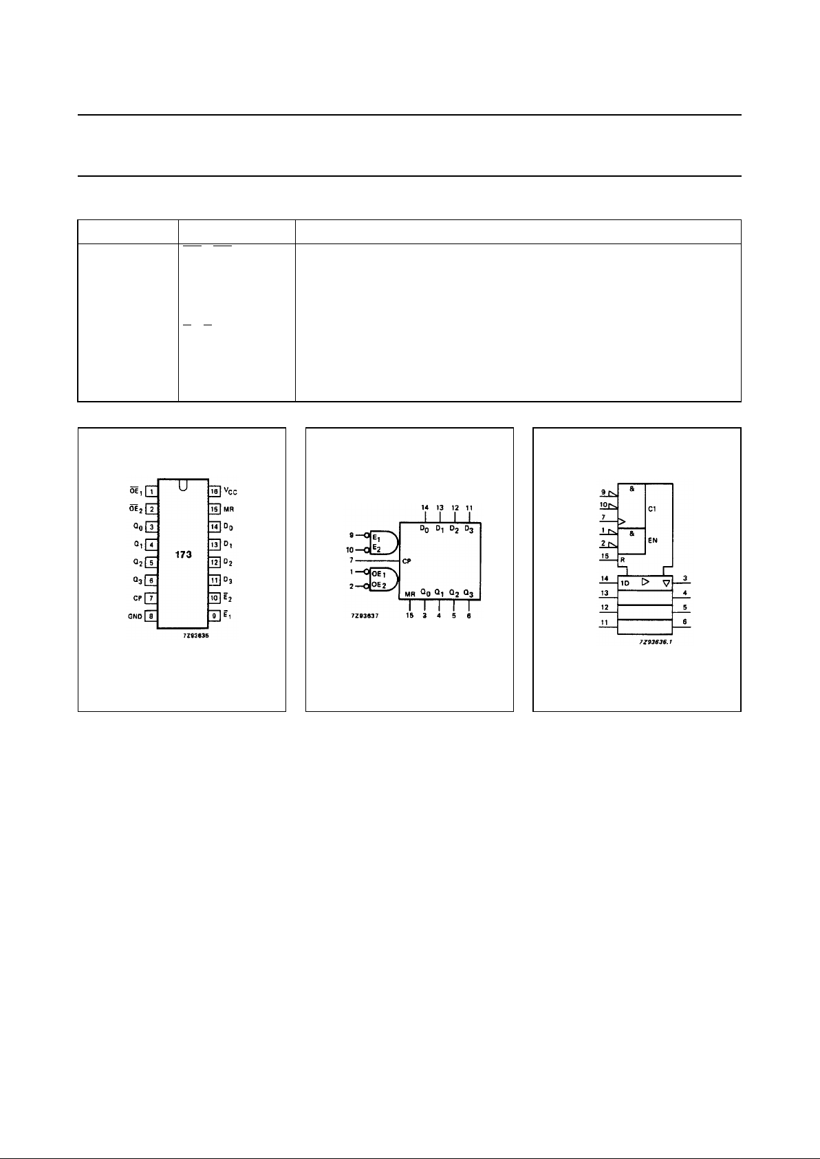
PIN DESCRIPTION
PIN NO. SYMBOL NAME AND FUNCTION
1, 2
OE1, OE
2
output enable input (active LOW)
3, 4, 5, 6 Q
0
to Q
3
3-state flip-flop outputs
7 CP clock input (LOW-to-HIGH, edge-triggered)
8 GND ground (0 V)
9, 10
E1, E
2
data enable inputs (active LOW)
14, 13, 12, 11 D
0
to D
3
data inputs
15 MR asynchronous master reset (active HIGH)
16 V
CC
positive supply voltage
Fig.1 Pin configuration. Fig.2 Logic symbol. Fig.3 IEC logic symbol.
Page 4
December 1990 4
Philips Semiconductors Product specification
Quad D-type flip-flop; positive-edge trigger; 3-state 74HC/HCT173
FUNCTION TABLE
Notes
1. H = HIGH voltage level
h = HIGH voltage level one set-up time prior to the LOW-to-HIGH CP transition
L = LOW voltage level
I = LOW voltage level one set-up time prior to the LOW-to-HIGH CP transition
q = lower case letters indicate the state of the referenced input (or output)
one set-up time prior to the LOW-to-HIGH CP transition
X = don’t care
Z = high impedance OFF-state
↑ = LOW-to-HIGH CP transition
REGISTER OPERATING MODES
INPUTS OUTPUTS
MR CP E1E2D
n
Qn (register)
reset (clear) H X X X X L
parallel load
LL↑
↑
lll
l
l
h
L
H
hold (no change)
LLX
X
hXXhX
X
q
n
q
n
3-STATE BUFFER OPERATING MODES
INPUTS OUTPUTS
Qn (register) OE1OE2Q0Q1Q2Q
3
read
L
H
L
L
LLLHLHLHL
H
disabled
X
X
HXXHZZZZZZZ
Z
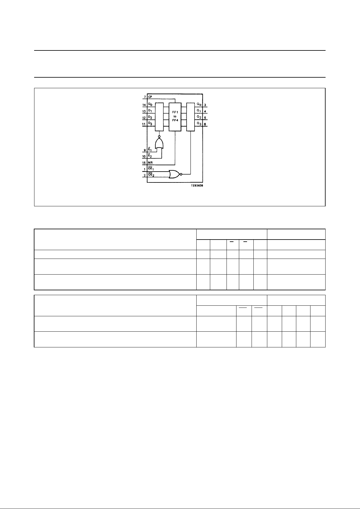
Fig.4 Functional diagram.
Page 5
December 1990 5
Philips Semiconductors Product specification
Quad D-type flip-flop; positive-edge trigger; 3-state 74HC/HCT173
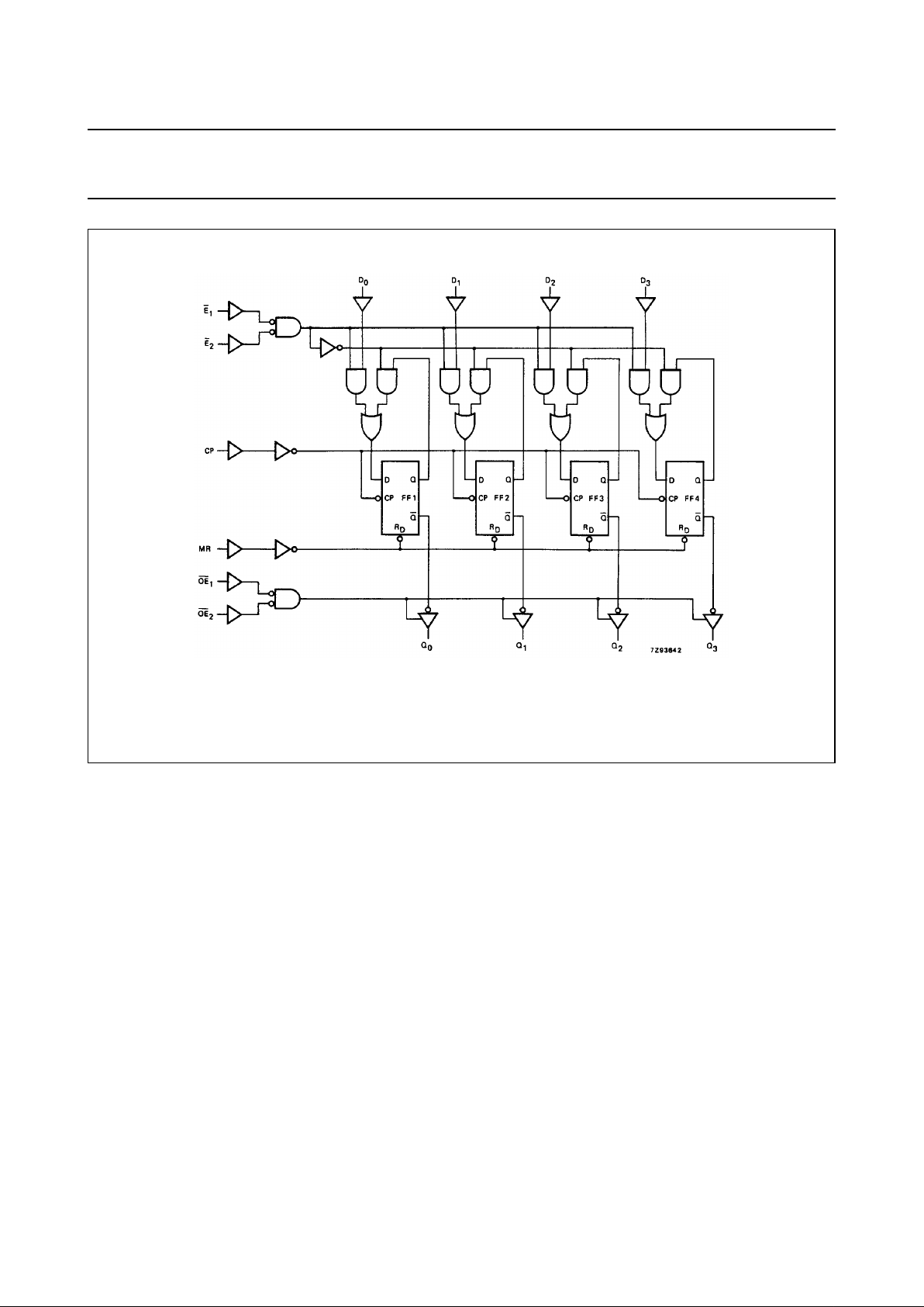
Fig.5 Logic diagram.
Page 6
December 1990 6
Philips Semiconductors Product specification
Quad D-type flip-flop; positive-edge trigger; 3-state 74HC/HCT173
DC CHARACTERISTICS FOR 74HC
For the DC characteristics see
“74HC/HCT/HCU/HCMOS Logic Family Specifications”
.
Output capability: bus driver
ICC category: MSI
AC CHARACTERISTICS FOR 74HC
GND = 0 V; t
r=tf
= 6 ns; CL=50pF
SYMBOL PARAMETER
T
amb
(°C)
UNIT
TEST CONDITIONS
74HC
V
CC
(V)
WAVEFORMS
+25 −40 to +85 −40 to +125
min. typ. max. min. max. min. max.
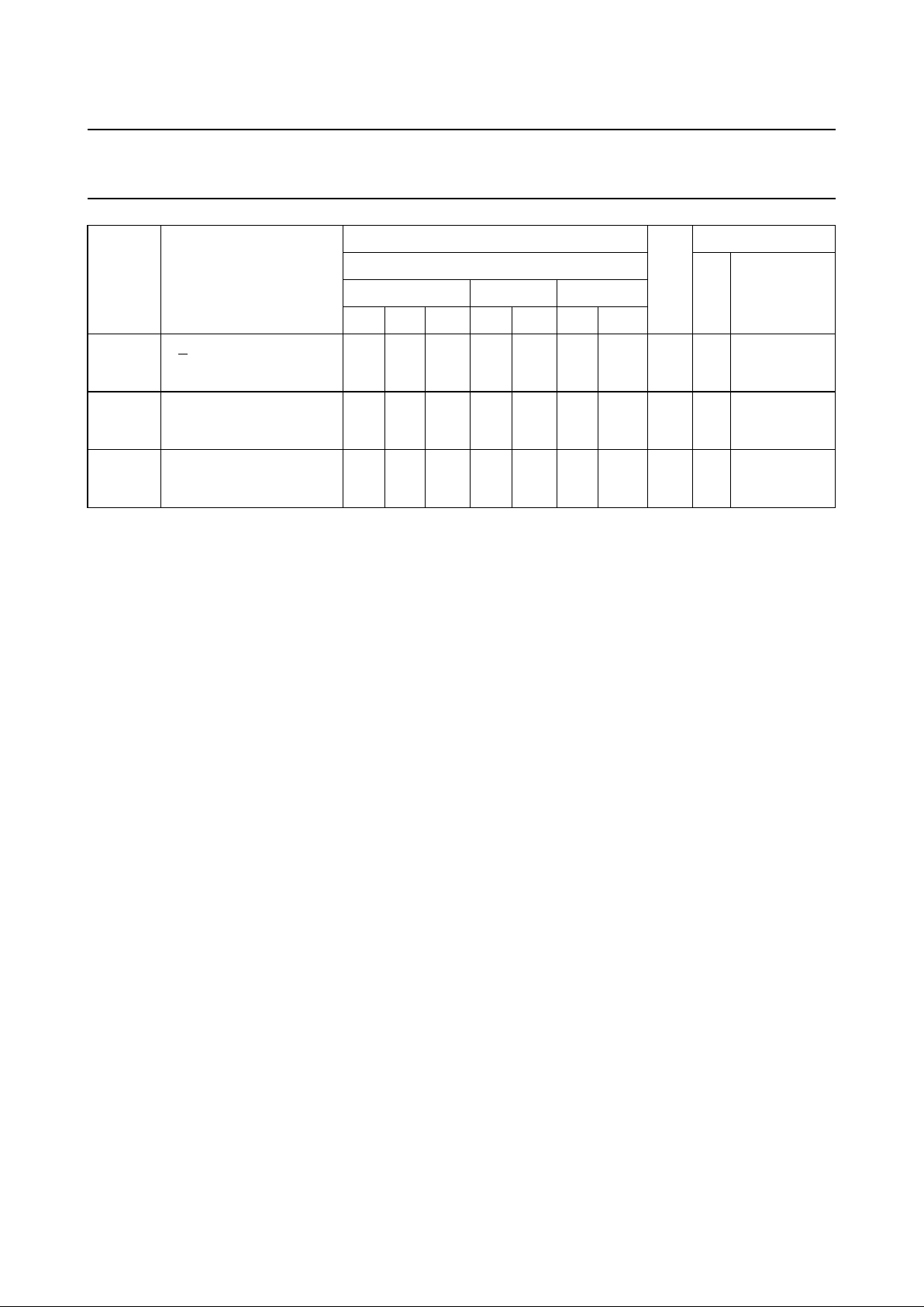
t
PHL
/ t
PLH
propagation delay
CP to Q
n
55
20
16
175
35
30
220
44
37
265
53
45
ns 2.0
4.5
6.0
Fig.6
t
PHL
propagation delay
MR to Q
n
44
16
13
150
30
26
190
38
33
225
45
38
ns 2.0
4.5
6.0
Fig.7
t
PZH
/ t
PZL
3-state output enable time
OEn to Q
n
52
19
15
150
30
26
190
38
33
225
45
38
ns 2.0
4.5
6.0
Fig.8
t
PHZ
/ t
PLZ
3-state output disable time
OEn to Q
n
52
19
15
150
30
26
190
38
33
225
45
38
ns 2.0
4.5
6.0
Fig.8
t
THL
/ t
TLH
output transition time 14
5
4
60
12
10
75
15
13
90
18
15
ns 2.0
4.5
6.0
Fig.6
t
W
clock pulse width
HIGH or LOW
80
16
14
14
5
4
100
20
17
120
24
20
ns 2.0
4.5
6.0
Fig.6
t
W
master reset pulse
width; HIGH
80
16
14
14
5
4
100
20
17
120
24
20
ns 2.0
4.5
6.0
Fig.7
t
rem
removal time
MR to CP
60
12
10
−8
−3
−2
75
15
13
90
18
15
ns 2.0
4.5
6.0
Fig.7
t
su
set-up time
En to CP
100
20
17
33
12
10
125
25
21
150
30
26
ns 2.0
4.5
6.0
Fig.9
t
su
set-up time
Dn to CP
60
12
10
17
6
5
75
15
13
90
18
15
ns 2.0
4.5
6.0
Fig.9
Page 7
December 1990 7
Philips Semiconductors Product specification
Quad D-type flip-flop; positive-edge trigger; 3-state 74HC/HCT173
t
h
hold time
En to CP
0
0
0
−17
−6
−5
0
0
0
0
0
0
ns 2.0
4.5
6.0
Fig.9
t
h
hold time
Dn to CP
1
1
1
−11
−4
−3
1
1
1
1
1
1
ns 2.0
4.5
6.0
Fig.9
f
max
maximum clock pulse
frequency
6.0
30
35
26
80
95
4.8
24
28
4.0
20
24
MHz 2.0
4.5
6.0
Fig.6
SYMBOL PARAMETER
T
amb
(°C)
UNIT
TEST CONDITIONS
74HC
V
CC
(V)
WAVEFORMS
+25 −40 to +85 −40 to +125
min. typ. max. min. max. min. max.
Page 8
December 1990 8
Philips Semiconductors Product specification
Quad D-type flip-flop; positive-edge trigger; 3-state 74HC/HCT173
DC CHARACTERISTICS FOR 74HCT
For the DC characteristics see
“74HC/HCT/HCU/HCMOS Logic Family Specifications”
.
Output capability: bus driver
ICC category: MSI
Note to HCT types
The value of additional quiescent supply current (∆I
CC
) for a unit load of 1 is given in the family specifications.
To determine ∆ICC per input, multiply this value by the unit load coefficient shown in the table below.
INPUT UNIT LOAD COEFFICIENT
OE1,OE
2
MR
E1, E
2
D
n
CP
0.50
0.60
0.40
0.25
1.00
Page 9
December 1990 9
Philips Semiconductors Product specification
Quad D-type flip-flop; positive-edge trigger; 3-state 74HC/HCT173
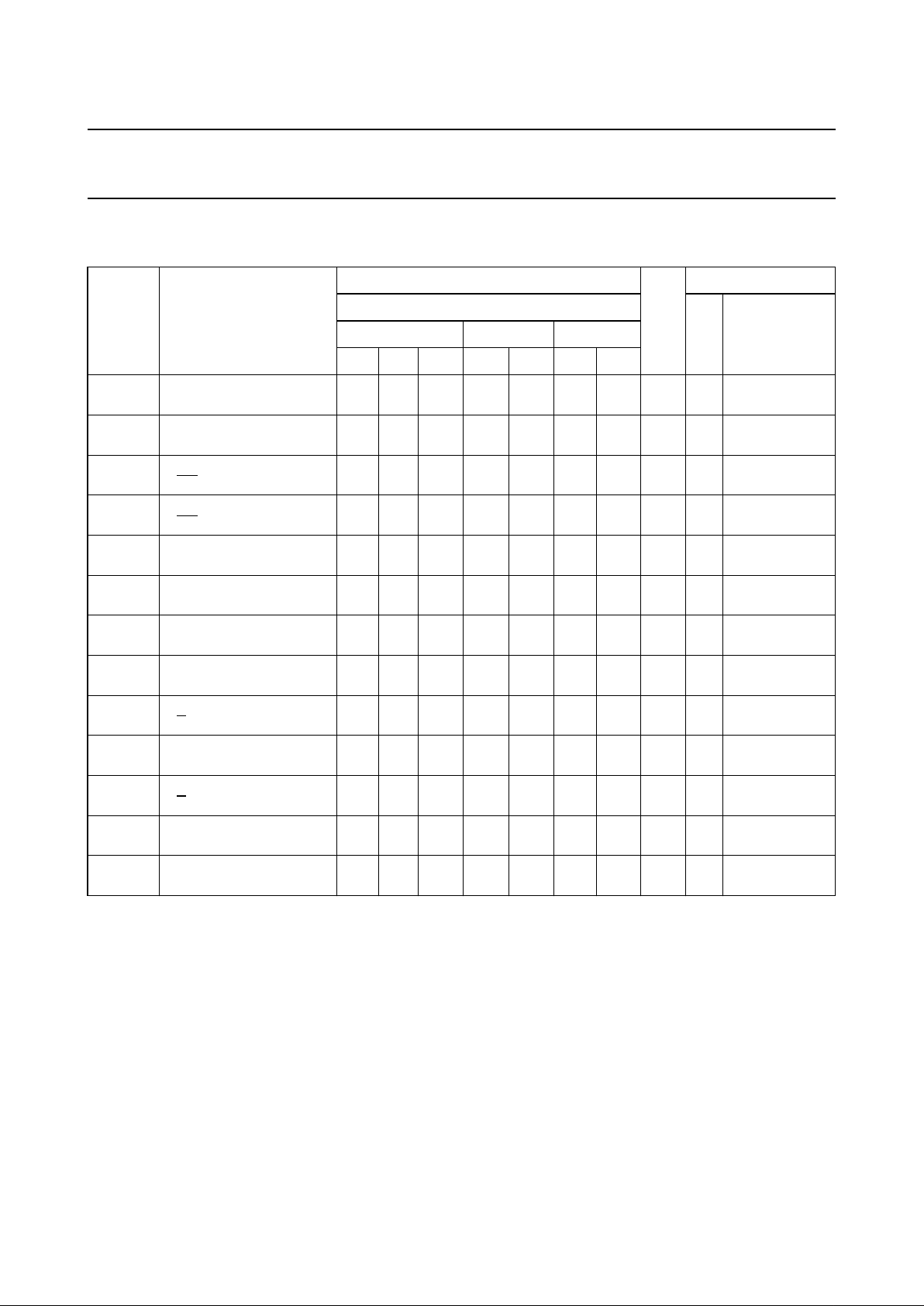
AC CHARACTERISTICS FOR 74HCT
GND = 0 V; t
r=tf
= 6 ns; CL=50pF
SYMBOL PARAMETER
T
amb
(°C)
UNIT
TEST CONDITIONS
74HCT
V
CC
(V)
WAVEFORMS
+25 −40 to +85 −40 to +125
min. typ. max. min. max. min. max.
t
PHL
/ t
PLH
propagation delay
CP to Q
n
20 40 50 60 ns 4.5 Fig.6
t
PHL
propagation delay
MR to Q
n
20 37 46 56 ns 4.5 Fig.7
t
PZH
/ t
PZL
3-state output enable time
OEn to Q
n
20 35 44 53 ns 4.5 Fig.8
t
PHZ
/ t
PLZ
3-state output disable time
OEn to Q
n
19 30 38 45 ns 4.5 Fig.8
t
THL
/ t
TLH
output transition time 5 12 15 19 ns 4.5 Fig.6
t
W
clock pulse width
HIGH or LOW
16 7 20 24 ns 4.5 Fig.6
t
W
master reset pulse
width; HIGH
15 6 19 22 ns 4.5 Fig.7
t
rem
removal time
MR to CP
12 −2 15 18 ns 4.5 Fig.7
t
su
set-up time
En to CP
22 13 28 33 ns 4.5 Fig.9
t
su
set-up time
Dn to CP
12 7 15 18 ns 4.5 Fig.9
t
h
hold time
En to CP
0 −6 0 0 ns 4.5 Fig.9
t
h
hold time
Dn to CP
0 −3 0 0 ns 4.5 Fig.9
f
max
maximum clock pulse
frequency
30 80 24 20 MHz 4.5 Fig.6
Page 10
December 1990 10
Philips Semiconductors Product specification
Quad D-type flip-flop; positive-edge trigger;
3-state
74HC/HCT173
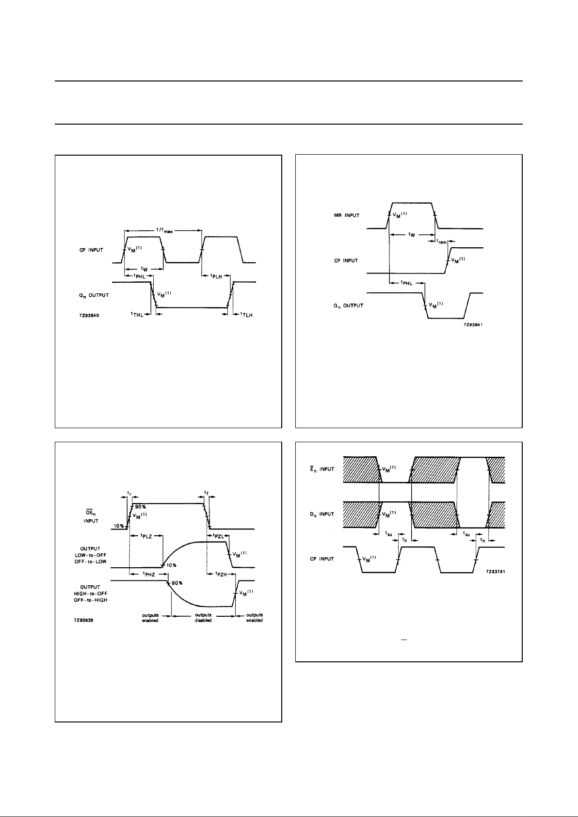
AC WAVEFORMS
Fig.6 Waveforms showing the clock (CP) to
output (Qn) propagation delays, the clock
pulse width, the output transition times and
the maximum clock pulse frequency.
(1) HC : VM= 50%; VI= GND to VCC.
HCT: V
M
= 1.3 V; VI= GND to 3 V.
Fig.7 Waveforms showing the master reset (MR)
pulse width, the master reset to output (Qn)
propagation delays and the master reset to
clock (CP) removal time.
(1) HC : VM= 50%; VI= GND to VCC.
HCT: V
M
= 1.3 V; VI= GND to 3 V.
Fig.8 Waveforms showing the 3-state enable and
disable times.
(1) HC : VM= 50%; VI= GND to VCC.
HCT: V
M
= 1.3 V; VI= GND to 3 V.
PACKAGE OUTLINES
See
“74HC/HCT/HCU/HCMOS Logic Package Outlines”
.
Fig.9 Waveforms showing the data set-up and hold
times from input (En, Dn) to clock (CP).
The shaded areas indicate when the input is permitted to
change for predictable output performance.
(1) HC : V
M
= 50%; VI= GND to VCC.
HCT: V
M
= 1.3 V; VI= GND to 3 V.
 Loading...