

Page 1
DATA SH EET
Product specification
File under Integrated Circuits, IC06
December 1990
INTEGRATED CIRCUITS
74HC/HCT164
8-bit serial-in/parallel-out shift
register
For a complete data sheet, please also download:
•The IC06 74HC/HCT/HCU/HCMOS Logic Family Specifications
•The IC06 74HC/HCT/HCU/HCMOS Logic Package Information
•The IC06 74HC/HCT/HCU/HCMOS Logic Package Outlines
Page 2
December 1990 2
Philips Semiconductors Product specification
8-bit serial-in/parallel-out shift register 74HC/HCT164
FEATURES
• Gated serial data inputs
• Asynchronous master reset
• Output capability: standard
• ICC category: MSI
GENERAL DESCRIPTION
The 74HC/HCT164 are high-speed Si-gate CMOS devices
and are pin compatible with low power Schottky TTL
(LSTTL). They are specified in compliance with JEDEC
standard no. 7A.
The 74HC/HCT164 are 8-bit edge-triggered shift registers
with serial data entry and an output from each of the eight
stages.
Data is entered serially through one of two inputs (D
sa
or
Dsb); either input can be used as an active HIGH enable for
data entry through the other input.
Both inputs must be connected together or an unused
input must be tied HIGH.
Data shifts one place to the right on each LOW-to-HIGH
transition of the clock (CP) input and enters into Q0, which
is the logical AND of the two data inputs (Dsa,Dsb) that
existed one set-up time prior to the rising clock edge.
A LOW level on the master reset (MR) input overrides all
other inputs and clears the register asynchronously,
forcing all outputs LOW.
QUICK REFERENCE DATA
GND = 0 V; T
amb
= 25 °C; tr= tf= 6 ns
Notes
1. C
PD
is used to determine the dynamic power dissipation (PDin µW):
PD= CPD× V
CC
2
× fi+∑(CL× V
CC
2
× fo) where:
fi= input frequency in MHz
fo= output frequency in MHz
∑ (CL× V
CC
2
× fo) = sum of outputs
CL= output load capacitance in pF
VCC= supply voltage in V
2. For HC the condition is VI= GND to V
CC
For HCT the condition is VI= GND to VCC− 1.5 V
ORDERING INFORMATION
See
“74HC/HCT/HCU/HCMOS Logic Package Information”
.
SYMBOL PARAMETER CONDITIONS
TYPICAL
UNIT
HC HCT
t
PHL
/ t
PLH
propagation delay
CP to Q
n
MR to Q
n
CL= 15 pF; VCC= 5 V
12
11
14
16
ns
ns
f
max
maximum clock frequency 78 61 MHz
C
I
input capacitance 3.5 3.5 pF
C
PD
power dissipation capacitance per
package
notes 1 and 2
40 40 pF
Page 3
December 1990 3
Philips Semiconductors Product specification
8-bit serial-in/parallel-out shift register 74HC/HCT164
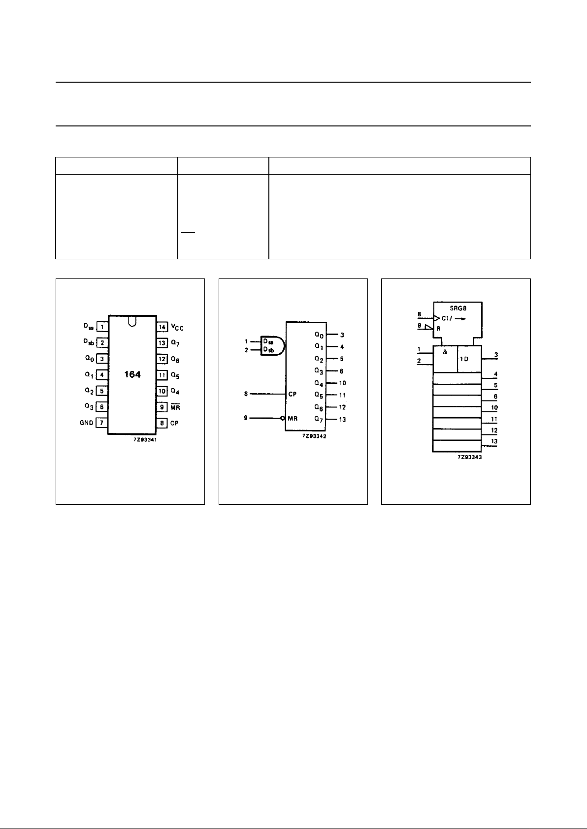
PIN DESCRIPTION
PIN NO. SYMBOL NAME AND FUNCTION
1, 2 D
sa,Dsb
data inputs
3, 4, 5, 6, 10, 11, 12, 13 Q
0
to Q
7
outputs
7 GND ground (0 V)
8 CP clock input (LOW-to-HIGH, edge-triggered)
9
MR master reset input (active LOW)
14 V
CC
positive supply voltage
Fig.1 Pin configuration. Fig.2 Logic symbol.
Fig.3 IEC logic symbol.
Page 4

December 1990 4
Philips Semiconductors Product specification
8-bit serial-in/parallel-out shift register 74HC/HCT164
APPLICATIONS
• Serial data transfer
FUNCTION TABLE
Note
1. H = HIGH voltage level
h = HIGH voltage level one set-up time prior to the LOW-to-HIGH clock transition
L = LOW voltage level
I = LOW voltage level one set-up time prior to the LOW-to-HIGH clock transition
q = lower case letters indicate the state of the referenced input one set-up time prior to the
LOW-to-HIGH clock transition
↑ = LOW-to-HIGH clock transition
OPERATING MODES
INPUTS OUTPUTS
MR CP D
sa
D
sb
Q
0
Q1− Q
7
reset (clear) L X X X L L − L
shift
H
H
H
H
↑
↑
↑
↑
l
l
h
h
l
h
l
h
L
L
L
H
q
0
− q
6
q0− q
6
q0− q
6
q0− q
6
Fig.4 Functional diagram.
Fig.5 Logic diagram.
Page 5

December 1990 5
Philips Semiconductors Product specification
8-bit serial-in/parallel-out shift register 74HC/HCT164
DC CHARACTERISTICS FOR 74HC
For the DC characteristics see
“74HC/HCT/HCU/HCMOS Logic Family Specifications”
.
Output capability: standard
ICCcategory: MSI
AC CHARACTERISTICS FOR 74HC
GND = 0 V; t
r
= tf= 6 ns; CL= 50 pF
SYMBOL PARAMETER
T
amb
(°C)
UNIT
TEST CONDITIONS
74HC
V
CC
(V)
WAVEFORMS
+25 −40 to +85 −40 to +125
min. typ. max. min. max. min. max.
t
PHL
/ t
PLH
propagation delay
CP to Q
n
41
15
12
170
34
29
215
43
37
255
51
43
ns 2.0
4.5
6.0
Fig.6
t
PHL
propagation delay
MR to Q
n
39
14
11
140
28
24
175
35
30
210
42
36
ns 2.0
4.5
6.0
Fig.6
t
THL
/ t
TLH
output transition
time
19
7
6
75
15
13
95
19
16
110
22
19
ns 2.0
4.5
6.0
Fig.6
t
W
clock pulse width
HIGH or LOW
80
16
14
14
5
4
100
20
17
120
24
20
ns 2.0
4.5
6.0
Fig.6
t
W
master reset pulse
width; LOW
60
12
10
17
6
5
75
15
13
90
18
15
ns 2.0
4.5
6.0
Fig.6
t
rem
removal time
MR to CP
60
12
10
17
6
5
75
15
13
90
18
15
ns 2.0
4.5
6.0
Fig.6
t
su
set-up time
Dsa, Dsbto CP
60
12
10
8
3
2
75
15
13
90
18
15
ns 2.0
4.5
6.0
Fig.6
t
h
hold time
Dsa,Dsbto CP
4
4
4
−6
−2
−2
4
4
4
4
4
4
ns 2.0
4.5
6.0
Fig.6
f
max
maximum clock
pulse frequency630
35
23
71
85
5
24
28
4
20
24
MHz 2.0
4.5
6.0
Fig.6
Page 6

December 1990 6
Philips Semiconductors Product specification
8-bit serial-in/parallel-out shift register 74HC/HCT164
DC CHARACTERISTICS FOR 74HCT
For the DC characteristics see
“74HC/HCT/HCU/HCMOS Logic Family Specifications”
.
Output capability: standard
ICCcategory: MSI
Note to HCT types
The value of additional quiescent supply current (∆I
CC
) for a unit load of 1 is given in the family specifications.
To determine ∆ICCper input, multiply this value by the unit load coefficient shown in the table below.
AC CHARACTERISTICS FOR 74HCT
GND = 0 V; t
r
= tf= 6 ns; CL= 50 pF
INPUT UNIT LOAD COEFFICIENT
Dsa,D
sb
CP
MR
0.25
0.60
0.90
SYMBOL PARAMETER
T
amb
(°C)
UNIT
TEST CONDITIONS
74HCT
V
CC
(V)
WAVEFORMS
+25 −40 to +85 −40 to +125
min. typ. max. min. max. min. max.
t
PHL
/ t
PLH
propagation delay
CP to Q
n
17 36 45 54 ns 4.5 Fig.6
t
PHL
propagation delay
MR to Q
n
19 38 48 57 ns 4.5 Fig.6
t
THL
/ t
TLH
output transition time 7 15 19 22 ns 4.5 Fig.6
t
W
clock pulse width
HIGH or LOW
18 7 23 27 ns 4.5 Fig.6
t
W
master reset pulse
width; LOW
18 10 23 27 ns 4.5 Fig.6
t
rem
removal time
MR to CP
16 7 20 24 ns 4.5 Fig.6
t
su
set-up time
Dsa,Dsbto CP
12 6 15 18 ns 4.5 Fig.6
t
h
hold time
Dsa,Dsbto CP
4 −2 4 4 ns 4.5 Fig.6
f
max
maximum clock pulse
frequency
27 55 22 18 MHz 4.5 Fig.6
Page 7

December 1990 7
Philips Semiconductors Product specification
8-bit serial-in/parallel-out shift register 74HC/HCT164
AC WAVEFORMS
Fig.6 Waveforms showing the clock (CP) to output (Qn) propagation delays, the clock pulse width, the output
transition times and the maximum clock frequency.
(1) HC : VM= 50%; VI= GND to VCC.
HCT : V
M
= 1.3 V; VI= GND to 3 V.
Fig.7 Waveforms showing the master reset (MR) pulse width, the master reset to output (Qn) propagation
delays and the master reset to clock (CP) removal time.
(1) HC : VM= 50%; VI= GND to VCC.
HCT : V
M
= 1.3 V; VI= GND to 3 V.
Fig.8 Waveforms showing the data set-up and hold times for Dninputs.
(1) HC : VM= 50%; VI= GND to VCC.
HCT : V
M
= 1.3 V; VI= GND to 3 V.
Page 8

December 1990 8
Philips Semiconductors Product specification
8-bit serial-in/parallel-out shift register 74HC/HCT164
PACKAGE OUTLINES
See
“74HC/HCT/HCU/HCMOS Logic Package Outlines”
.
 Loading...